

Page 1
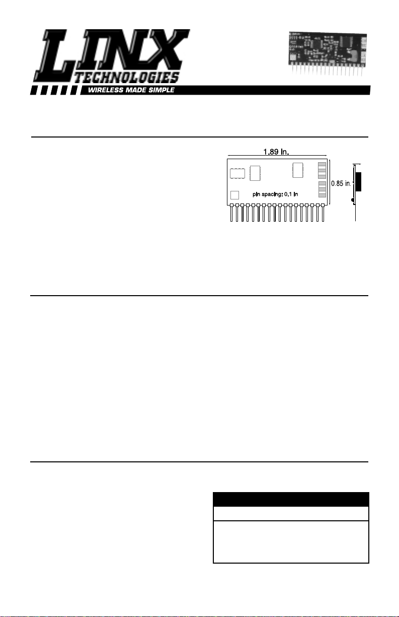
Page 1
HP SERIES-II RECEIVER MODULE DESIGN GUIDE
APPLICATIONS INCLUDE:
■ Continuous Data Transfer
■ Home/Industrial Automation
■ Wireless Networking
■ Remote Control
■ Remote Access
■ Remote Monitoring/Telemetry
■ Fire/Security Alarms
■ Long-Range RFID
■ High-Quality Wireless Audio
■ Analog Signal Transfer
■ General Wire Elimination
FEATURES:
■ 8 Binary Selectable Reception Frequencies
■ Exceptional Sensitivity (-95dBm @ 10-5BER typical)
■ High Serial Data Rate (50Kbps max.)
■ Direct Serial Interface
■ Fully Qualified Data Output
■ Wide-Range Audio-Capable Analog Output (50Hz-25KHz)
■ Cost-Effective
■ No External RF Components Required (Except Antenna)
■ Manufacturing-Friendly SIP-Style Packaging
■ Precision-Synthesized Frequency Reference
■ Wide Supply Range (2.7-16V DC)
■ Receive Signal Strength (RSSI) and Powerdown Pins
■ No Production Tuning
DESCRIPTION:
The HP Series-II receiver module is designed for the
cost-effective, high-performance wireless transfer of
analog or digital data, in the popular 902-928MHz
band. The receiver offers eight selectable channels
and, when paired with an HP Series-II transmitter, is
capable of receiving analog and digital information
for distances up to 1000 feet (under optimum
conditions). The receiver employs an advanced
microprocessor-controlled synthesized architecture.
Like all Linx modules, the HP Series-II requires no
tuning and in most cases no external RF
components
(except an antenna), making
integration straightforward even for engineers
lacking previous RF experience.
PART # DESCRIPTION
MDEV-900-HP-II Evaluation Kit 900 MHz
TXM-900-HP-II Transmitter 900 MHz
RXM-900-HP-II Receiver 900 MHz
ANTENNA
GND
GND
GND
GND
GND
GND
GND
N/C
CH SELECT 0
CH SELECT 1
CH SELECT 2
POWER DOWN
RSSI
GND
VCC
ANALOG OUT
DATA OUT
123456789
101112131415161718
0.35
Figure 1: Physical Package
ORDERING INFORMATION
HIGH PERFORMANCE
RF MODULE
RXM-900-HP-II
Revised 2/1/00
Page 2
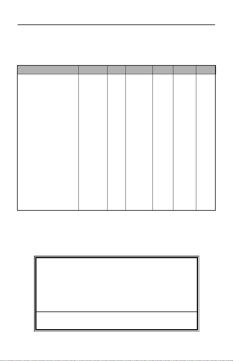
Absolute Maximum Ratings:
Supply voltage Vcc -0.3 to 18 VDC
Operating temperature 0°C to +70°C
Storage temperature -45°C to +85°C
Soldering temperature +260°C for 15 sec.
RF input, pin 1 0 dBm
*NOTE* Exceeding any of the limits of this section may lead to permanent
damage to the device. Furthermore, extended operation at these maximum
ratings may reduce the life of this device.
Page 2
Parameter Designation Min. Typical Max. Units Notes
Input Voltage V
CC
2.7 – 16.0 Volts –
Supply Current I
CC
16 18 20 mA 1
Sleep Current I
SLP
–– 50 µA –
Data output:
Logic low V
DOL
GND – 0.5 VDC –
Logic high V
DOH
VCC-.3 – V
CC
VDC –
RF input impedance R
IN
– 50 – Ohms –
Receive frequency F
C
903.37 – 921.37 MHz 2
Noise Bandwidth N
3DB
– 280 – KHz –
Data Bandwidth 300 – 50,000 Bps –
Audio Bandwidth 50 – 25,000 Hz –
Sensitivity -92 -95 -100 dBm 3
DC Modulation Sensitivity -88 ––dBm 4
RSSI:
Dynamic Range 60 70 80 dB –
Gain G
RSSI
– 24 – mV/dB –
Voltage/No Carrier –– 1.6 mV –
Spurious Emmissions –– -45 dBm –
Interference Rejection:
Half FCSpurious – 60 – dB –
F
C
±1MHz – 20 – dB –
SPECIFICATIONS
1. Over full operating voltage
2. Depends on CS0 - CS2 voltage levels
3. For 10
-5
BER @ 9600 bps
4. Minimum input power level to ensure that data output can hold a DC level
Figure 2: Specifications table
Notes:
ABOUT THESE MEASUREMENTS
The performance parameters listed below are based on module operation at
25°C from a 5VDC supply unless otherwise noted. It is recommended all ground
pins be connected to the ground-plane. The pin marked N/C has no physical
connection and is designed only to add support.
Figure 3: Maximum ratings table
Page 3
Page 3
2.40
2.10
1.80
1.50
1.20
0.90
0.60
0.30
0.00
-110 -100 -80 -70 -60 -50 -40
RSSI Out
(V)
PIN (dBm)
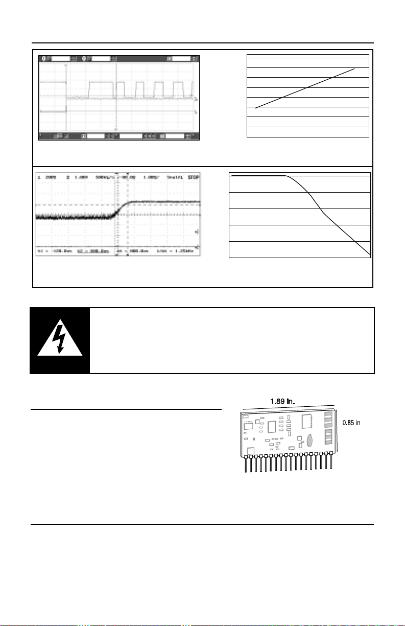
Figure 6: RSSI Response Time
Figure 4: Receiver Turn-on Time
Figure 7: BER vs. Input Power (typical)
Figure 8: Physical package
1
-6
1
-5
1
-4
1
-3
1
-2
1
-90 -91 -92 -93 -94 -95 -96 -97 -98 -99 -100
BER
PIN (dBm)
Figure 5: Receiver RSSI
TYPICAL PERFORMANCE GRAPHS
PON
Data Out
PHYSICAL PACKAGING
The receiver is packaged as a hybrid
through-hole SIP-style module with 18
pins spaced at .1” intervals. Baseband
components occupy the rear of the board
while high-frequency components are
grouped on the front.Pin 1 is on the f ar left
of the board when viewed from the front.
PRODUCTION CONSIDERATIONS
The SIP module may be installed using hand- or wave-solder techniques. The
module should not be subjected to reflow. If the module is subject to production
wash cycles, adequate drying time should be allowed prior to power-up. If the
wash cycle introduces contaminants, the module’s performance may be
adversely affected.
*CA UTION*
This product incorporates numerous static-sensitive components.
Always wear an ESD wrist strap and observe proper ESD handling
procedures when working with this device. Failure to observe this
precaution may result in module damage or failure.
2.00 V/div 5.00 V/div +/-1.0 V
2.00 ms/div
6.57000000 ms 2.58 V
Page 4

Page 4
HP-II RECEIVER MANUAL TIMING CONSIDERATIONS
There are five major timing considerations the engineer must be aware of when
designing with the HP Series-II receiver.These are shown in figure 8A below, and
are labeled T1through T5.
Parameter Description Min. Max.
T
1
Carrier turn-on 5 mSec
settling time
T
2
Max time between 33 mSec
data output transitions
T
3
Max Channel 10 mSec
Change Time (Time to
Valid Data)
T
4
Receiver Turn-on Time 12 mSec
T
5
Receiver Off Time 1 mSec
T
1
While the HP-II transmitter is turned off (i.e., the receiver is not receiving a
carrier), the receiver's output is squelched.When the HP-II transmitter is turned
on, there is a finite time between the power-up of the transmitter and the
transmitter being on-channel.This is known as the transmitter power-up time.
Once the transmitter is on-channel, its CTS line goes high indicating that the
transmitter is ready to send data. However, at this time the receiver is not ready
to receive data.It takes some time for the receiver to settle once the CTS pin on
the transmitter is high.This time is shown in figure 8A as
T1.
In short, T1is the maximum time required for the data output of the receiver to
be valid once the transmitter's CTS pin goes high.This assumes that the receiver
is already powered up.
T
2
The minimum baud rate of the HP-II receiver is 300 baud, assuming that the serial
data is 10 bits, including a start and stop bit, each of opposite polarity.Therefore,
even if the data itself was all 1’s or all 0’s, the star t and stop bit would create a
transition every 10 bits (or once ev ery 33mSec).If a transition does not occur in the
33mSec time, and the power lev el presented at the receiv er's RF input is abov e the
DC modulation sensitivity, the data output will go high and remain high until the
next byte. Once the minimum baud rate has been violated, though, the first byte
transmitted after the delay will be in error if any of the lower 4 bits are 0's.
The designer must either guarantee that there will never be a delay of more than
33mSec between transitions on the transmitter’s data input pin or must always
send a 255 (or FF hex) follo wing a delay of more than 33mSec. See applications
note AN-00160 for more information.
T3-T5are self-explanatory
Figure 8A: Time Considerations Table
Page 5
Page 5
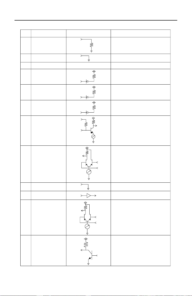
PIN# Name Equivalent CTK Description
50-ohm RF Input
Analog Ground
No Connection
RF Input/
Antenna Input
Gnd
RF In
Channel Select 0CS0
CS0
Channel Select 1CS1
CS1
Channel Select 2
Received Signal
Strength Indicator
Digital Ground
Voltage Input 2.7-16V
1V p-p Analog Output
Digital Data Output
Power down
(Active Low)
CS2
CS2
PDN
RSSI
RSSI
Gnd
VCC
Analog Out
Data Out
N/C
1
2-8
9
10
11
12
13
14
15
16
17
18
50Ω
4.7K
VIN
PDN
470K
V
IN
10K
10K
10K
PIN DESCRIPTIONS:
Figure 9: Pin functions and equivalent circuits
Page 6
Page 6
THEORY OF OPERATION
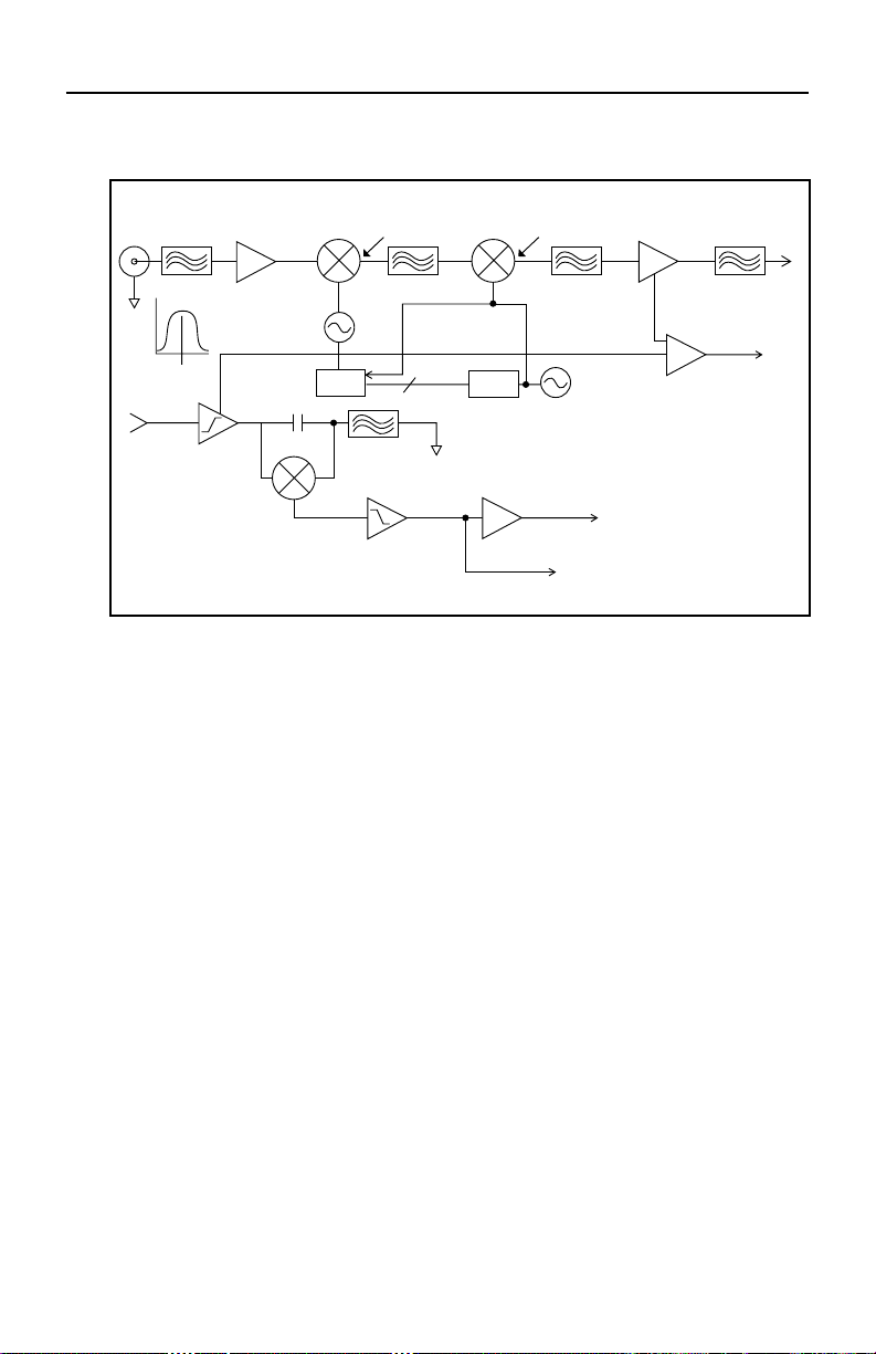
The HP-II-RXM is a high-performance, eight-channel, dual-conversion superhet
FM receiver capable of receiving analog or digital data.
Digital information is modulated at the transmitter using FSK (frequency shift
keying), the binary form of frequency modulation. FSK offers significant
advantages over AM-based modulation methods, i.e., increased noise immunity
and the ability of the receiver to “capture” in the presence of multiple signals.
These advantages will be particularly appreciated in crowded bands like those in
which the HP-II operates. While FSK modulation is not the most bandwidthefficient manner of modulating digital data, it is an excellent choice for reliable,
low-cost, low-power RF products such as the HP Series-II.
To transmit analog information the module employs FM modulation.In this mode,
simple to complex waveforms can be introduced at the transmitter’s data pin and
recovered with minimal distortion at the receiver’s analog output pin.
The user-supplied antenna is connected at pin 1 (see Figure 1).The HP-II-RXM
RF port is matched to 50 ohms to support interface to commonly available
antennas such as those manufactured by Linx.
The RF signal coming in from the antenna is filtered by a SAW (surface acoustic
wave) filter. The purpose of the SAW BPF is to attenuate unwanted RF energy
(i.e., not in the 902-928 MHz band) that is present at the antenna.A SAW device
provides significantly steeper roll-off and higher out-of-band attenuation than
other filter types such as an LC bandpass.
Once filtered by the SAW, the signal is then amplified by a Low-Noise Amplifier
(LNA) to increase the receiver sensitivity and lower the overall noise figure of the
receiver. After the LNA, the signal is mixed with a synthesized local oscillator to
perform the first frequency conversion.
Figure 10: HP Series-II Receiver Block Diagram
SAW BPF
902-928 MHz
915 MHz
LIMITING
AMP
LNA IF
868-887 MHz
(See Table)
VCO
PLL µP
10.7 MHz FM
Discriminator
1
34.7 MHz BPF
18 KHz
Active
LPF
BitPERFECT™
BIT SLICER
IF
2
XTO
AUDIO
DATA
AMP
IF
10.7 MHz BPF10.7 MHz BPF
RSSI
Page 7

Page 7
BOARD LAYOUT CONSIDERATIONS
If you are at all familiar with RF devices you may be concerned about
specialized layout requirements. Fortunately, because of the care taken by
Linx in the layout of the module’s PCB, integrating an HP Series-II receiver
into your design is very straightforward. By adhering carefully to a few basic
design and layout rules, you can enjoy a trouble-free path to RF success.
Figure 11 shows the
suggested PCB footprint for
the HP Series-II receiver.
A ground-plane (as large as
possible) should be placed
directly under the HP-II
receiver. This ground-plane
can also be critical to the
performance of your
antenna.
The first IF frequency is 34.7 MHz. This frequency is achieved by setting the
synthesizer frequency to a value that is lower than the incoming RF energy from
the antenna.
A high-performance IF receiver strip is used to perform the second conversion
and the FM demodulation. The IF strip takes the 34.7 MHz frequency from the
first conversion, mixes it with a high-precision 24.0 MHz crystal oscillatorgenerated frequency to produce the second IF of 10.7 MHz, and amplifies it in
preparation for FM demodulation.
FM demodulation is achieved with an on-board gilbert multiplier.The output of
the IF strip is a demodulated wavef orm that, after filtering, very closely resembles
the original waveform used to modulate the transmitter.
A high-performance, active low-pass filter cleans up the audio signal, removing
all of the unwanted noise from the FM demodulation process.The output of this
filter is provided to the audio output pin and to the BitPERFECT bit slicer, which
uses proprietary methods to suppor t a wide dynamic range of modulation rates
(300 bps to 50Kbps) with no prerequisites for waveform duty cycle.
An on-board micro-controller is used to manage receiver functions and to provide
a simple interface to external circuitry .The micro-controller performs the following
functions:
- FREQUENCY SYNTHESIZER PROGRAMMING: The micro-controller reads
the three-channel select input lines and programs the frequency synthesizer
registers to the proper values for a given channel. This frees the user from
complex programming requirements and allows for manual channel selection via
switches in product designs where a microprocessor is not used.
- BASEBAND DATA QUALIFICATION: The micro-controller monitors the signal
quality and squelches the data output when the signal is not strong enough for
accurate data detection. This prevents noise on the data output pin during
low-signal or no-signal conditions.
.060"
.10"
.060"
.030" Dia. Finished
Figure 11: Suggested PCB Footprint
Page 8
Page 8
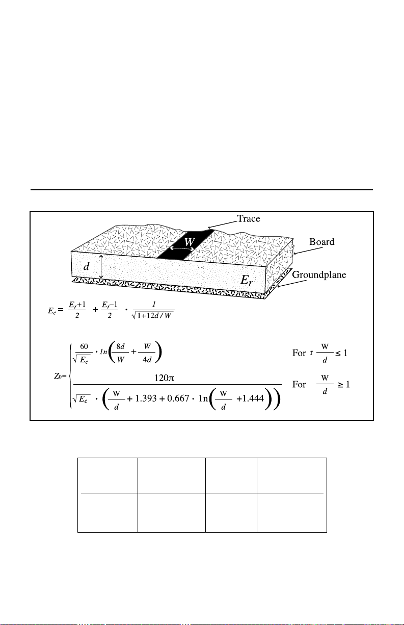
Figure 12: Microstrip formulas (Er = Dielectric constant of PCB material)
MICROSTRIP DETAILS
The HP-II receiver should, as much as reasonably possible, be isolated from all
other components on your PCB. Specifically, high-frequency circuitry such as
crystal oscillators should be kept as far away as possible from the HP-II receiver.
If the receiver is to be mounted parallel to the board, it should be laid ov er so that
the side with the crystal is closest to the PC board and the RF side is facing away
from the PC board.
The trace from the receiver to the antenna should be kept as short as possible.
A simple trace is suitable for runs up to 1/4 inch for antennas with wide bandwidth
characteristics. For longer runs or to avoid detuning a high-Q narrow bandwidth
antenna such as a helical, use a 50-ohm coax or 50-ohm microstrip transmission
line as shown below.
Effective
Dielectric Width/Height Dielectric Characteristic
Constant (W/d) Constant Impedance
4.8 1.8 3.59 50.0
4 2 3.07 51.0
2.55 3 2.12 48.0
Page 9
Page 9
POWER CONSIDERATIONS
POWER SUPPLY
The user must provide a clean source of power to the receiver to ensure proper
operation. In an FM receiver, power-supply noise will manifest itself as AM and
FM noise in the receiver circuitry, reducing the
overall sensitivity of the receiver. Providing a
good power supply for the module is a
designer’s first line of defense in the battle for
receiver sensitivity.
The HP-II-RXM incorporates a precision LowDropout Regulator on-board which allows the
module to operate over an input voltage range
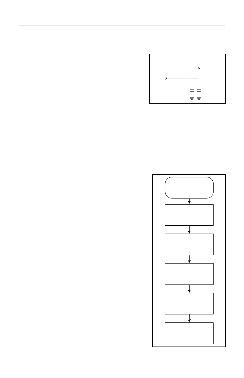
of 2.7 to 16 volts DC. The module’s powersupply line should have low ESR bypass
capacitors configured as shown in fig. 13.
POWER UP SEQUENCE
The HP-II-RXM is controlled by an on-board microprocessor. When power is
applied, a start-up sequence is executed. At the end of the start-up sequence,
the receiver is ready to receive data.
Figure 14 shows the start-up sequence.This sequence is executed when power
is applied to the VCC pin or when the PDN pin is cycled from low to high.
On power-up, the microprocessor reads the
external channel-selection lines and sets the
frequency synthesizer to the appropriate
channel. Once the frequency synthesizer has
locked on to the selected channel’s frequency,
the receiver is ready to accept data.
Figure 4 on Pg. 3 shows the typical turn-on
response time for an HP Series-II receiver. The
response time was measured by connecting the
module’s RF input to a signal generator which is
set to the proper channel frequency with an
output power of -80dBm and FM modulated at
50kHz deviation with a 1kHz square wave. You
will notice that the data output remains squelched
until the internal start-up procedure has been
executed and the receiver is ready to receive
data.
The HP-II-RXM can be put into an ultra-lowcurrent (<50uA) power-down mode by holding
the PDN pin low. If the PDN pin is left floating or
held high, the receiver will turn fully on. In powerdown mode, the receiver is completely shut
down.Thus, the RSSI circuit CANNOT be used to
monitor for channel activity.
Figure 14: Start-up sequence
Figur e 13:Suggested supply filter
V
IN
cc
Crystal Oscillator
Begins to Operate
Read Channel-
Selection Inputs
V
cc
module
POWER ON
Squelch Data
Output Pin
Program
Frequency
Synthesizer
Go To
Main Loop
to
.1µF>22µF
Page 10
Page 10
CHANNEL SELECTION
The HP-II receiver module features eight user-selectable channels. The channel
of operation is determined by the state of pins CS0-CS2. Figure 15 shows a
channel-selection table based
on the pins’ states. The onboard microprocessor performs
all PLL loading functions. This
frees the user from complex
programming requirements and
allows for manual channel
selection via switches in product
designs where a microprocessor
is not used.
ANALOG OUTPUT
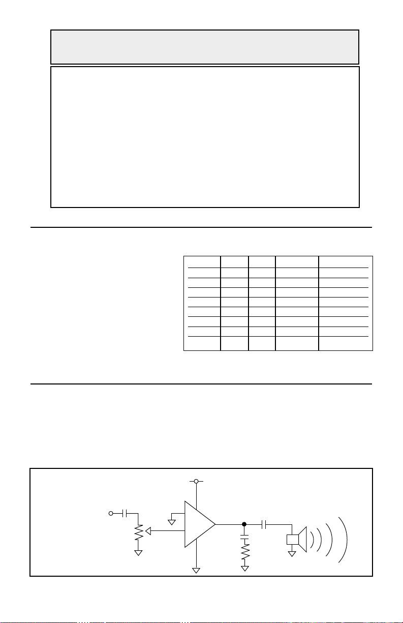
The analog output is derived after amplification in the BitPERFECT bit slicer.The
analog output is valid from 50 Hz to 25 KHz, providing an AC signal of about 1V
peak-to-peak.This output should not be used to drive a low-impedance load such
as a speaker. In applications requiring direct drive into a speaker, such as the
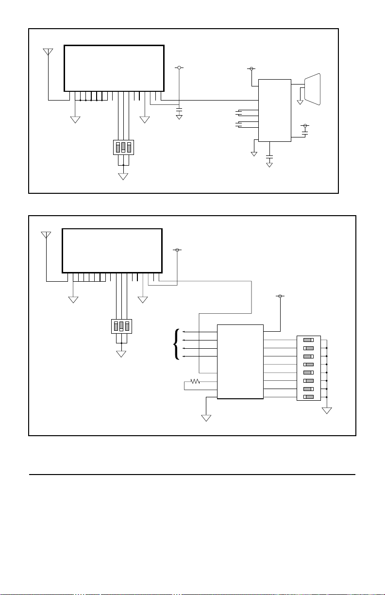
transmission of audio, a simple op-amp circuit like the one shown in Figure 16
can be used.In this circuit, the op-amp is used to act as an impedance converter.
HP Analog Out
10K
6
2
3
+
-
4
LM386
8
.05uF
1uF
250uF
10
4-12V
Figure 16: Audio Amplifier
A common method of reducing receiver power consumption is to turn the receiver off
via the PDN pin for some time interval and wake the receiv er periodically to check for
the presence of a transmitted signal. In order to implement this method with an HP-II
receiver successfully, there are some timing requirements the user must observe
when powering up the receiver to check for channel activity.
At power-up the receiver’s on-board microprocessor will begin its start-up routine as
detailed previously. A 12 mSec time period must be allotted to allow this routine to be
completed. After 12 mSec, the data and RSSI circuits are fully qualified and reliable.
The off-period is determined by the discharge rate of the internal bypass capacitors.
The capacitors must fully discharge to ensure that subsequent power-ups will reliably
restart the microprocessor.This minimum time should be no less than 1 mSec. If the
user is finding that the transmitter is not reliable starting up after power-up, this time
should be increased.
NOTE:
READ THIS IF YOU ARE GOING TO PERIODICALLY
POWER-DOWN RECEIVER!!
CS2 CS1 CS0 Channel Frequency
0 0 0 0 903.37
0 0 1 1 906.37
0 1 0 2 907.87
0 1 1 3 909.37
1 0 0 4 912.37
1 0 1 5 915.37
1 1 0 6 919.87
1 1 1 7 921.37
Figure 15: Channel-Selection Table
Page 11

THE DATA OUTPUT
Once a reliable RF link has been established, the challenge becomes how to
effectively transfer data across it. While a properly designed RF link provides
reliable data transfer under most conditions, there are still distinct differences from
a wired link that must be addressed. Since the HP-II modules do not incorporate
internal coding/decoding, a user has tremendous flexibility in how data is handled.
The data output is generated by an on-board open-collector comparator and
swings from 0V (representing the reception of a logic “0”) to VIN (representing a
logic “1”). This output is capable of sinking 2 mA of current and presents a 4.7K
source resistance when sourcing current. If additional current sourcing or sinking
capacity is required, the user should use a buffer gate to service the additional
loads.
When a carrier is not present, the data output is continuously high. Although the
audio output of the receiver is pure noise, an internal squelch circuit is used to hold
the data output low. The data output will “break squelch” anytime the RF energy
present at the antenna input is strong enough to cause the RSSI voltage to rise
above the factory-set squelch level. Typically, a receiver will only break squelch
when a carrier is present on the desired frequency. However, strong signals at
interfering frequencies can also cause the data output to break squelch.
When a carrier is present with no modulation, the data output will remain
continuously high when the RF signal input level is above the DC Modulation
Sensitivity. Note that the DC modulation sensitivity is higher than the data
sensitivity of the receiver. The ability to maintain a DC level on the data output
requires a higher SNR than is required to receive data. When the RF signal input
level is below the DC modulation sensitivity but above the data sensitivity, the
receiver’s output will contain valid data when the incoming carrier is modulated.
However, in this condition the receiver may not hold a continuous high level on the
data output when the carrier is not being modulated.
This feature is unique to the HP Series-II and is designed to support direct
operation with UARTs which require their input to be continuously marking (or
high). The HP Series-II transmitters and receivers can be directly connected
between two UARTs without the need for buffering or logical inversion.
Another area of consideration is that of data structure or protocol. If you are not
familiar with the considerations for sending serial data in a wireless environment
you will want to review Linx application note #00160 (Considerations for sending
data with the HP Series-II). These issues should be clear ly understood prior to
commencing a significant design effort.
If you want to transfer simple control or status signals such as button presses or
switch closures, and your product does not have a microprocessor on board your
product or you wish to avoid protocol de v elopment, consider using an encoder and
decoder IC set. These chips are available from a wide range of manufacturers
including: Microchip (Keeloq), Holtek, and Motorola. These chips take care of all
encoding, error checking, and decoding functions and generally provide a number
of data pins to which switches can be directly connected.In addition, address bits
are usually provided for security and to allow the addressing of multiple receivers
independently. These IC’s are an excellent way to bring basic Remote
Control/Status products quickly and inexpensively to market. Additionally, it is a
simple task to interface with inexpensive microprocessors such as the Microchip
PIC or one of many IR, remote control, DTMF, and modem IC’s.
Page 11
Page 12
Page 12
ANTENNA
GND
GND
GND
GND
GND
GND
GND
N/C
CH SELECT 0
CH SELECT 1
CH SELECT 2
POWER DOWN
RSSI
GND
VCC
ANALOG
DATA OUT
123456789
101112131415161718
1
2
3
4
5
6
7
8
9
D0
D1
D2
D3
VT
DIN
OSC1
OSC2
GND
VCC
A7
A6
A5
A4
A3
A2
A1
A0
18
17
16
15
14
13
12
11
10
Channel
Select
RX1
S1
3-Position
DIP Switch
Output
to User
U2
HT694
S2
8-Position
DIP Switch
Address Select
390K
Figure 18: Typical Application - Remote-Control Receiver
PROXIMITY OPERATION
If modules are combined to form a transceiver they should be operated in halfduplex, meaning that only the transmitter or receiver is active at any time.When
combined with certain high-gain antennas the HP-II transmitter can, in close
proximity, exceed -10dBm power into the receiver. Since the receiver does not
incorporate an AGC this can result in poor performance or complete shutdown
of the receiver .This effect occurs when both the transmitter and receiver hav e the
high-gain antennas connected and are in close proximity (1-5 feet) of each other.
ANTENNA
GND
GND
GND
GND
GND
GND
GND
N/C
CH SELECT 0
CH SELECT 1
CH SELECT 2
POWER DOWN
RSSI
GND
VCC
ANALOG
DATA OUT
123456789
101112131415161718
7
16
+
+
+
+
+
C1
4.7 uF
C4
4.7 uF
C2
4.7 uF
C3
4.7 uF
C5
220 uF
Channel
Select
RX1
3 Position
DIP Switch
10
1
3
4
5
6
2
15
2
J1
DB-9F
U2
MAX 232
5
Figure 17: Typical Application - RS-232 Interface
Page 13

Page 13
RSSI CIRCUIT
The HP Series-II receivers are equipped with an on-board Received-SignalStrength-Indicator (RSSI) circuit.RSSI is useful to check for channel occupation,
and interference as well as signal strength determination.
The RSSI circuit provides a DC voltage which is logarithmically proportional to
the incoming signal strength present at the RF input pin.The RSSI circuit has a
voltage range of about 800mV to 2.5 V and a dynamic signal range of better
than 60 dB.
Figure 5 on p. 3 shows the RSSI output versus input signal strength. This graph
is a characterization only and is adapted from measurements made from a small
sampling of receivers.The RSSI response is different for every FM-IF chip, and
is therefore different for every HP Series-II receiver. Calibration parameters are
stored on-board to compensate for this variation.
Figure 6 on p. 3 shows the RSSI response time with an input power of -80dBm.
This graph basically shows how long it takes the RSSI voltage to respond to an
instantaneous increase in output power. If the carr ier is AM modulated, or OOK
modulated (in the case of data), the RSSI pin can be used for demodulation.
If your application requires that you accurately measure the incoming signal
strength (distance measurement, for example), then you must calibrate the
RSSI circuit on a receiver-by-receiver basis.
The calibration process is simple.Using a signal generator, inject a -40dBm
unmodulated carrier into the receiver and measure the RSSI voltage.
Repeat the same for an input signal level of -100dBm. This is known as a
two-point “slope” calibration.
To determine the slope of the RSSI response, use the following equation:
M=60/(V2-V1)
Where M=slope in dB/volts
V1=the voltage measured at -100dBm
V2=the voltage measured at -40dBm
Using this slope, you can determine the signal strength for any RSSI
voltage using the following formula:
SS=M * (V
1
-Vm) +100dBm
Where SS=signal strength in dBm
M=previously determined slope
Vm=measured RSSI voltage
If you are using a microprocessor with an A/D converter, this process can
easily be achieved in software .If not, it can also be achieved using standard
analog measurement circuitry.
NOTE: MAKING SIGNAL STRENGTH MEASUREMENTS
WITH THE RSSI CIRCUIT
Page 14
Page 14
RECEIVER SENSITIVITY PERFORMANCE
The sensitivity of a receiver is critical to the overall range-performance of a
wireless link. Among wireless manufacturers this measurement is particularly
subject to specmanship due to the variety of methods and conditions under
which sensitivity can be tested.
A hallmark of Linx designs is outstanding sensitivity, but more importantly our
sensitivity specifications are based on harsh testing. The receiver sensitivity for
the HP Series-II is specified for a given bit-error-rate (BER), which is measured
using a pseudo-random bitstream generated by a bit-error-rate-tester (BERT). A
sample of each lot of modules is tested for sensitivity, and therefore the quoted
sensitivity is a characterization of the module, and not a guaranteed
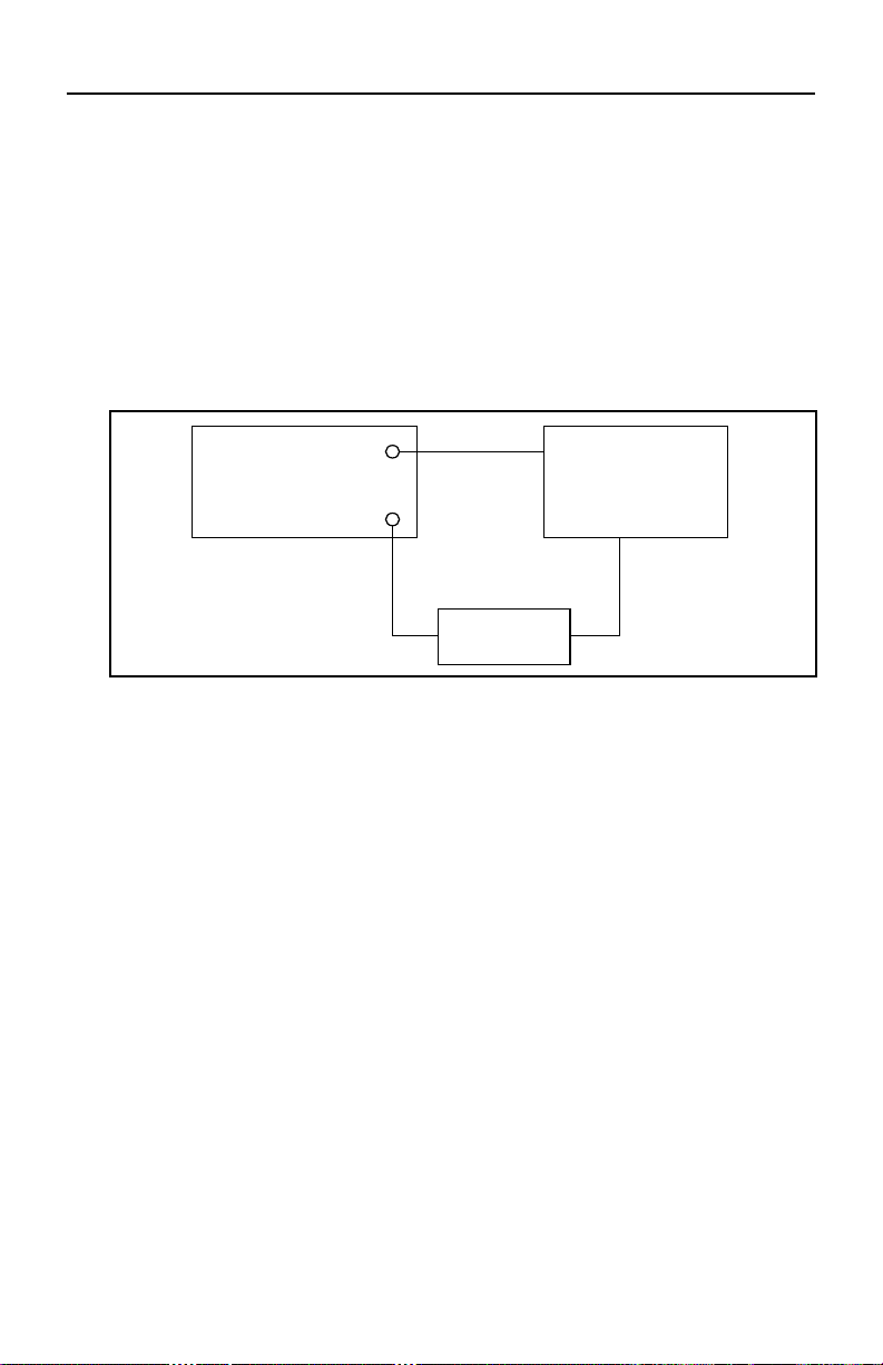
specification. The receiver sensitivity test setup used by Linx is shown in the
figure below.
Figure 7 on page 3 shows the typical BER versus input power for the HP SeriesII receivers.This graph can be used to determine the actual sensitivity you can
attain for a given application.For instance, high-rate data communications w ould
require a BER of <1
-5
where a low-rate data application with redundant data
transmission may only require a BER of <1
-2
.
Based on the sensitivity characterization of the HP-II receiver and the output
power of the transmitter as legally allowed by the FCC, a path loss model can be
used to show that the open field range of an HP-II link can exceed 1,000 f eet.The
actual ability of a particular product utilizing the HP Series-II receivers to attain
this range-performance depends on many factors including:
1). Quality of receiving antenna
2). Actual path loss model (open field, inter-building, city, etc.)
3). Quality of power supply
The HP-II development kit you purchased contains two development boards that
can be used to properly evaluate an HP-II data link's range-performance. If you
have any difficulties duplicating the same range with your own product, you
should carefully review all Linx documentation for hints on what the problem
might be.If all else fails, contact Linx and discuss your design with an application
engineer.
Figure 19: Sensitivity Test Setup
RF
IN
TXD OUT
HP Receiver
Under Test
Phoenix 5500
BER Tester
RxD
IN
Data
Out
Hewlett Packard ES-3000
Signal Generator
EXT 1
RF Out
Page 15

Page 15
ANTENNA CONSIDERATIONS
The choice of antennas is one of the most critical and often overlooked design
considerations. The range, performance, and legality of an RF link is critically
dependent upon the type of antenna employed. Proper design and matching of
an antenna is a complex task requiring sophisticated test equipment and a
strong background in principles of RF propagation. While adequate antenna
performance can often be obtained by trial and error methods, you may also w ant
to consider utilizing a professionally designed antenna such as those offered by
Linx. Our low-cost antenna line is designed to ensure maximum performance
and compliance with Part 15 attachment requirements. The purpose of the
following sections is to give you a basic idea of some of the considerations
involved in the design and selection of antennas. For a more comprehensive
discussion please review Linx applications note #00500 “Antennas: Design,
Application, Performance”.
THE TRANSMITTER ANTENNA
The transmitter antenna allows RF energy to be efficiently radiated from the
output stage into free space. In modular designs such as the HP, a transmitter’s
output power is often slightly higher than the legal limit.This allows a designer to
utilize an inefficient antenna in order to achieve full legal power while meeting
size, cost, or cosmetic objectives. For this reason a transmitter's antenna can
generally be less efficient than the antenna used on the receiver.
THE RECEIVER ANTENNA
A receiving antenna should give its optimum performance at the frequency or in
the band for which a receiver was designed, and capture as little as possible of
other off-frequency signals.The efficiency of the receiver’s antenna is critical to
maximizing range-performance. Unlike the transmitter antenna, where legal
operation may mandate a reduction in antenna efficiency or attenuation, the
receiver’s antenna should be optimized as much as is practical.
It is usually best to utilize a basic quarter-wave whip for your initial concept
evaluation. Once the prototype product is operating satisfactorily, a production
antenna should be selected to meet the cost, size and cosmetic requirements of
the product.
Maximum antenna efficiency is always
obtained when the antenna is at
resonance. If the antenna is too short,
capacitive reactance is present; if it is
too long, inductive reactance will be
present. The indicator of resonance is
the minimum point in the VSWR curve.
You will see from the following example
that antenna (A) is resonant at too low
a frequency, indicating excessive
length, while antenna (C) is resonant at
too high a frequency, indicating the
antenna is too short. Antenna (B),
however, is “just right.”
AB C
DESIRED FREQUENCY
Page 16

Page 16
GENERAL ANTENNA RULES
The following general rules should help in maximizing antenna performance:
1. Proximity to objects such as a user’s hand or body, or metal objects will
cause an antenna to detune. For this reason the antenna shaft and tip
should be positioned as far away from such objects as possible.
2. Optimum performance will be obtained from a 1/4- or 1/2-wave straight whip
mounted at a right angle to the ground-plane. In many cases this isn’t
desirable for practical or ergonomic reasons; thus, an alternative antenna
style such as a helical, loop, patch, or base-loaded whip may be utilized.
3. If an internal antenna is to be used, keep it away from other metal
components, particularly large items like transformers, batteries, and PCB
tracks and ground-planes.In many cases, the space around the antenna is
as important as the antenna itself.
4. In many antenna designs, particularly 1/4-wave whips, the ground-plane
acts as a counterpoise, forming, in essence, a 1/2-wave dipole. For this
reason adequate ground-plane area is essential. As a general rule the
ground-plane to be used as counterpoise should have a surface area ≥ the
overall length of the 1/4-wave radiating element.
5. Remove the antenna as far as possible from potential interference sources.
Any frequency of sufficient amplitude to enter the receiver’s front end will
reduce system range, cause increased bit errors, and can even prevent
reception entirely. There are many possible sources of internally generated
interference. Switching power supplies, oscillators, even relays can also be
significant sources of potential interference. Here again, the single best
weapon against such problems is attention to placement and layout. Filter
the module’s power supply with a high-frequency bypass capacitor. Place
adequate ground-plane under all potential sources of noise. Shield noisy
board areas whenever practical.
6. In some applications it is advantageous to place the receiver and its
antenna away from the main equipment.This avoids interference problems
and allows the antenna to be oriented for optimum RF performance.Always
use 50Ω coax such as RG-174 for the remote feed.
Antenna resonance should not be confused with antenna impedance. The
difference between resonance and impedance is most easily understood by
considering the value of VSWR at its lowest point. The lowest point of VSWR
indicates the antenna is resonant, but the value of that low point is determined
by the quality of the match between the antenna, the transmission line, and the
device it is attached to.
To fully appreciate the importance of an antenna that is both resonant and
matched consider that an antenna with a VSWR of 1.5 will effectively transmit
approximately 95% of its power while an antenna with a VSWR of 10 will only
transmit about 30%. (See pg. 23)
Page 17
Page 17
ANTENNA STYLES
From a coat hanger to a tuned Yagi, there are literally hundreds of antenna styles
and variations that can be employed.Following is a brief discussion of the styles
most commonly utilized in compact RF designs. The selection chart broadly
categorizes key areas of antenna performance. In reviewing this section it is
important to recognize that each antenna style will produce widely varying
results based on the specific design execution and optimization. Additional
information can be found in Linx application notes #00500, #00100, #00125 and
#00140.
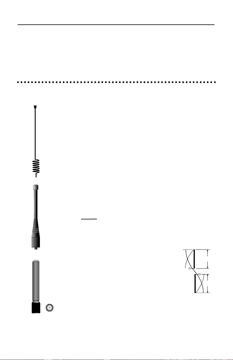
A whip-style antenna provides exceptional performance and is
easy to integrate.A low-cost whip is generally made of a wire or
rod while more expensive whip designs are encapsulated in
rubber or plastic to improve appearance and minimize the
potential for damage to the antenna element. A whip is often
combined with a helical winding to reduce the overall length.
This technique is commonly referred to as “base loading”.
Every frequency has a physical length that it occupies in space.
That length is referred to as the
wavelength and is theoretically
determined by two factors: 1) the frequency itself and 2) the
speed of propagation. The wavelength of the frequency to be
received or transmitted determines an antenna’s length. Since
an antenna has a dielectric constant greater than that of free
space, the velocity of a wa ve on the antenna is slo wer.This fact,
along with several other factors, has led antenna designers to
accept the formula below as an accurate starting point for
determining the physical length of a half-wave antenna. The
resultant length may be divided in half for a quarter wave.
Because of its compact length, a popular
antenna style for Part 15 applications is the
1/4-wave whip. It is important to note that in
order to operate effectively the 1/4 wave
must radiate against a ground-plane. The
ground-plane can be a metal case or
ground area on a PCB of at least equivalent
area to the antenna’s surface. The groundplane acts as a counterpoise, in essence
forming an effective half-wave dipole as
illustrated.
There are many manufacturers providing high-quality whip
antennas. It is important to remember, however, that Part 15
requires a permanent attachment or attachment with a unique
or not commonly available connector. This r ules out the use of
whips employing standard connectors such as BNC's.
Whip Style
1/4-wave wire lengths
for HP frequencies:
902-928MHz = 3.06"
L =
234
F
MHz
Where:
L=length in feet of quarter-wave length
F=operating frequency in megahertz
VERTICAL λ/4 GROUNDED
ANTENNA (MARCONI)
E
DIPOLE
ELEMENT
λ/4
I
GROUND
PLANE
VIRTUAL λ/4
DIPOLE
λ/4
Page 18
Page 18
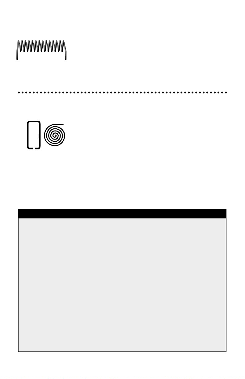
A loop or track-style antenna is usually printed directly on the
PCB making it the most cost-effective of antenna styles.There
are many different styles and shapes of loops which can be
utilized, including spirals and rectangles. A loop has excellent
immunity to proximity detuning (i.e., a user’s body) and is
easily concealed inside products which have a plastic case.
Despite these advantages a loop is difficult to match and tune
without expensive RF test equipment.An improperly designed
loop will have a very high SWR and may induce harmonics.For
this reason a helical or whip style is usually a better choice for
applications requiring maximum range-performance. For
products where cost or size is critical, a designer will generally want to have a loop
professionally designed and optimized.
PARAMETER LOOP HELICAL WHIP
Ultimate performance ● ●● ●●●
Ease of design setup ● ●● ●●●
Size ●● ●●● ●
Immunity to proximity effects ●●● ●● ●
HP-II Range (open ground to similar antenna) 400 ft. 600 ft. 1,000+ ft.
●=FAIR ●●=GOOD ●●●=EXCELLENT
HP Antenna Selection Chart
Helical Style
A helical is a wire coil usually wound from steel, copper or
brass. This antenna is very efficient given its small size. The
helical is an excellent choice for products requiring good
range-performance and a concealed internal antenna
element. Care must be exercised in placement, however, as a
helical detunes badly when located in proximity with other
conductive objects.Because a helical has a high "Q" factor its
bandwidth is very narrow and inter-coil spacing has a
pronounced effect on antenna performance. For this reason it
is usually best to utilize a premade helical which has been
professionally optimized to achieve maximum performance.
Loop Style
Page 19
Page 19
ANTENNA SHARING
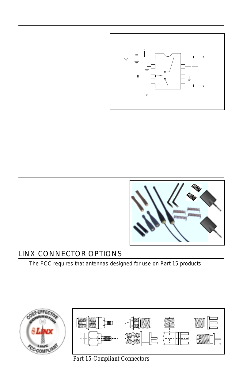
Many times when a transmitter
and receiver module are
combined to form a
transceiver the designer will
find it advantageous for the
modules to share a single
antenna.To accomplish this an
antenna switch must be used
to provide isolation between
each of the modules. There
are a wide variety of antenna
switches available which are
cost-effective and straightforward to use.Among the most
popular are switches from Alpha, Motorola, Philips, TriQuint, and NEC. Look for
an antenna switch that has high isolation and low loss at the desired frequency
of operation. Generally, the TX or RX status of a switch will be controlled by a
product’s microprocessor, but selection may also be made manually by the user.
In some cases where the characteristics of the TX and RX antennas need to be
different or switch losses are unacceptable the designer may find it more
practical to utilize two discrete antennas.
LINX ANTENNA OPTIONS
Linx offers a full line of antennas which
are optimized for the frequencies at
which our modules operate. The
antennas are cost-effectively priced in
volume and designed to maximize the
performance of your product. For
complete details,visit the Linx website at
www.linxtechnologies.com, or contact
the Linx literature department at
(800)736-6677.
Figure 20: Typical Antenna Switch
;
;
;;;
yyy
yyy
;
;
;;;
yyy
yyy
;
;
y
y
Part 15-Compliant Connectors
LINX CONNECTOR OPTIONS
The FCC requires that antennas designed for use on Part 15 products be either
permanently attached, or utilize a unique and proprietary connector not available
to the general public.Linx offers a full line of connectors designed to comply with
these requirements. To insure the continued compliance of these connectors,
details are not available on our website. However, complete connector
specifications may be obtained by contacting the Linx literature department at
(800)736-6677.
Antenna
0.1µF
0.1µF
V
DD
GND
Select
0.1µF
0.1µF
GND
0.1µF
Transmitter
Module
Receiver
Module
;
;;;;;;;;
yyyyyyyy
;;;;;;;;
yyyyyyyy
;
Page 20

Page 20
LEGAL CONSIDERATIONS
When working with RF, a clear distinction must be made between what is technically
possible and what is legally acceptable in the country where operation is intended.
Many manufacturers have avoided incorporating RF into their products as a result of
uncertainty and even fear of the approval and cer tification process. Here at Linx our
desire is not only to expedite the design process, but also to assist you in achieving
a clear idea of what is involved in obtaining the necessary approv als to legally market
your completed product.
In the United States the approval process is actually quite straightforward. The
regulations governing RF devices and the enforcement of them are the responsibility
of the Federal Communications Commission. The regulations are contained in the
Code of Federal Regulations (CFR), Title 47. Title 47 is made up of numerous
volumes; however, all regulations applicable to this module are contained in volume
0-19. It is strongly recommended that a copy be obtained from the Government
Printing Office in Washington, or from your local government book store. Excerpts of
applicable sections are included with Linx evaluation kits or ma y be obtained from the
Linx Technologies web site (www.linxtechnologies.com). In brief, these rules require
that any device which intentionally radiates RF energy be approved, that is, tested,
for compliance and issued a unique identification number .This is a relatively painless
process. Linx offers full EMC pre-compliance testing in our HP/Emco-equipped test
center. Final compliance testing is then performed by one of the many independent
testing laboratories across the country. Many labs can also provide other
certifications the product may require at the same time, such as UL, CLASS A/B, etc.
Once your completed product has passed, you will be issued an ID number which is
then clearly placed on each product manufactured.
Questions regarding interpretations of the Part 2 and Part 15 rules or measurement
procedures used to test intentional radiators, such as the HP-II modules, for
compliance with the Part 15 technical standards, should be addressed to:
Federal Communications Commission
Equipment Authorization Division
Customer Service Branch, MS 1300F2
7435 Oakland Mills Road
Columbia, MD 21046
Tel: (301) 725-1585 / Fax: (301) 344-2050 E-Mail: [email protected]
International approvals are slightly more complex, although many modules are
designed to allow all international standards to be met. If you are considering the
export of your product abroad, you should contact Linx Technologies to determine
the specific suitability of the module to your application.
All Linx modules are designed with the approval process in mind and thus much of
the frustration that is typically experienced with a discrete design is eliminated.
Approval is still dependent on many factors such as the choice of antennas, correct
use of the frequency selected, and physical packaging.While some extra cost and
design effort are required to address these issues, the additional usefulness and
profitability added to a product by RF makes the effort more than worthwhile.
NOTE: HP Series-II Modules are designed as component devices which
require external components to function. The modules are intended to allow for
full Part 15 compliance; how ev er, they are not approved by the FCC or any other
agency worldwide. The purchaser understands that approvals may be required
prior to the sale or operation of the device, and agrees to utilize the component
in keeping with all laws governing its operation in the country of operation.
Page 21
Page 21
SURVIVING AN RF IMPLEMENTATION
Adding an RF stage brings an exciting new dimension to
any product. It also means that additional effort and
commitment will be needed to bring the product
successfully to market. By utilizing premade RF
modules, such as the HP-II Series-II, the design and
approval process will be greatly simplified. It is still
important, however, to have an objective view of the
steps necessary to insure a successful RF integration.
Since the capabilities of each customer vary widely it is
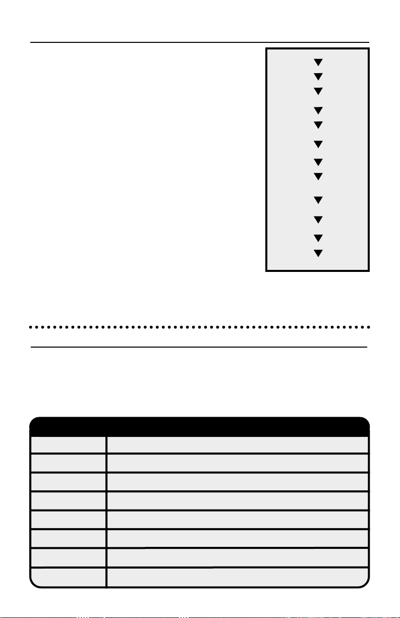
difficult to recommend one particular design path, but
most projects follow steps similar to those shown at the
right.
In reviewing this sample design path you may notice
that Linx offers a variety of services, such as
antenna design, and FCC prequalification, that are
unusual for a high-volume component manufacturer.
These services, along with an exceptional level of
technical support, are offered because we recognize
that RF is a complex science requiring the highest
caliber of products and support. “Wireless Made
Simple” is more than just a motto, it’s our
commitment. By choosing Linx as your RF partner
and taking advantage of the resources we offer, you
will not only survive implementing RF, but you may
even find the process enjoyable.
TYPICAL STEPS FOR
IMPLEMENTING RF
HELPFUL APPLICATION NOTES FROM LINX
It is not the intention of this manual to address in depth many of the issues that
should be considered to ensure that the modules function correctly and deliver
the maximum possible performance.As you proceed with your design you may
wish to obtain one or more of the following application notes, which address in
depth key areas of RF design and application of Linx products.
00500 Antennas: Design, Application, Performance
00130 Modulation techniques for low-cost RF data links
00126 Considerations for operation in the 902 Mhz to 928 Mhz band
00100 RF 101: Information for the RF challenged
00140 The FCC Road: Part 15 from concept to approval
00150 Use and design of T-Attenuation Pads
00110 Understanding the performance specifications of receivers
00160 Considerations for sending data with the HP Series-II
NOTE # LINX APPLICATION NOTE TITLE
DECISION TO UTILIZE RF IS MADE
RESEARCH RF OPTIONS
ORDER EVALUATION KIT(S)
TEST MODULE(S) WITH
BASIC HOOKUP
LINX MODULE IS CHOSEN
INTERFACE TO CHOSEN
CIRCUIT AND DEBUG
CONSULT LINX REGARDING
ANTENNA OPTIONS AND DESIGN
LAY OUT BOARD
SEND PRODUCTION-READY
PROTOTYPE TO LINX
FOR EMC PRESCREENING
OPTIMIZE USING RF SUMMARY
GENERATED BY LINX
SEND TO PART 15
TEST FACILITY
RECEIVE FCC ID #
COMMENCE SELLING PRODUCT
Page 22

Page 22
Power Conversion Tables For 50Ω System
dBm mW dBmV mVRMS mVp mVpp
-50 0.000 -3.0 0.7 1.0 2.0
-45 0.000 2.0 1.3 1.8 3.6
-40 0.000 7.0 2.2 3.2 6.3
-35 0.000 12.0 4.0 5.6 11.2
-30 0.001 17.0 7.1 10.0 20.0
-25 0.003 22.0 12.6 17.8 35.6
-20 0.0l 0 27.0 22.4 31.6 63.2
-15 0.032 32.0 39.8 56.2 112.5
-10 0.100 37.0 70.7 100.0 200.0
-5 0.316 42.0 125.7 177.8 355.7
0 1.000 47.0 223.6 316.2 632.5
1 1.259 48.0 250.9 354.8 709.6
2 1.585 49.0 281.5 398.1 796.2
3 1.995 50.0 315.9 446.7 893.4
4 2.512 51.0 354.4 501.2 1002.4
5 3.162 52.0 397.6 562.3 1124.7
6 3.981 53.0 446.2 631.0 1261.9
7 5.012 54.0 500.6 707.9 1415.9
8 6.310 55.0 561.7 794.3 1588.7
9 7.943 56.0 630.2 891.3 1782.5
10 10.000 57.0 707.1 1000.0 2000.0
11 12.589 58.0 793.4 1122.0 2244.0
12 15.849 59.0 890.2 1258.9 2517.9
13 19.953 60.0 998.8 1412.5 2825.1
14 25.119 61.0 1120.7 1584.9 3169.8
15 31.623 62.0 1257.4 1778.3 3556.6
16 39.811 63.0 1410.9 1995.3 3990.5
17 50.119 64.0 1583.0 2238.7 4477.4
18 63.096 65.0 1776.2 2511.9 5023.8
19 79.433 66.0 1992.9 2818.4 5636.8
20 100.000 67.0 2236.1 3162.3 6324.6
21 125.893 68.0 2508.9 3548.1 7096.3
22 158.489 69.0 2815.0 3981.1 7962.1
23 199.526 70.0 3158.5 4466.8 8933.7
24 251.189 71.0 3543.9 5011.9 10023.7
25 316.228 72.0 3976.4 5623.4 11246.8
26 398.107 73.0 4461.5 6309.6 12619.1
27 501.187 74.0 5005.9 7079.5 14158.9
28 630.957 75.0 5616.7 7943.3 15886.6
29 794.328 76.0 6302.1 8912.5 17825.0
30 1000.000 77.0 7071.1 10000.0 20000.0
Page 23

Page 23
VSWR Insertion Power Power
Loss Transmitted Reflected
(dB) (%) (%)
17.391 -6.87 20.57% 79.43%
11.610 -5.35 29.21% 70.79%
8.724 -4.33 36.90% 63.10%
6.997 -3.59 43.77% 56.23%
5.848 -3.02 49.88% 50.12%
5.030 -2.57 55.33% 44.67%
4.419 -2.20 60.19% 39.81%
3.946 -1.90 64.52% 35.48%
3.570 -1.65 68.38% 31.62%
3.010 -1.26 74.88% 25.12%
2.615 -0.97 80.05% 19.95%
2.323 -0.75 84.15% 15.85%
2.100 -0.58 87.41% 12.59%
1.925 -0.46 90.00% 10.00%
1.433 -0.14 96.84% 3.16%
1.222 -0.04 99.00% 1.00%
1.119 -0.01 99.68% 0.32%
1.065 0.00 99.90% 0.10%
1.034 0.00 99.97% 0.03%
1.020 0.00 99.99% 0.01%
MISMATCH CONVERSION TABLE
NOTES:
Page 24

Page 24
LINX TECHNOLOGIES, INC.
575 S.E. ASHLEY PLACE
GRANTS PASS, OR 97526
Phone: (541) 471-6256
FAX: (541) 471-6251
http://www.linxtechnologies.com
U.S. CORPORATE HEADQUARTERS:
Linx Technologies is continually striving to improve the quality and function of its products; for
this reason, we reserve the right to make changes without notice.The information contained in
this Data Sheet is believed to be accurate as of the time of pub lication.Specifications are based
on representative lot samples. Values may vary from lot to lot and are not guaranteed. Linx
Technologies makes no guarantee, warranty, or representation regarding the suitability of any
product for use in a specific application. None of these devices is intended for use in
applications of a critical nature where the safety of life or property is at risk.The user assumes
full liability for the use of product in such applications.Under no conditions will Linx Technologies
be responsible for losses arising from the use or failure of the device in any application, other
than the repair, replacement, or refund limited to the original product purchase price. Some
devices described in this publication are patented. Under no circumstances shall any user be
conveyed any license or right to the use or ownership of these patents.
Disclaimer
© 1999 by Linx Technologies, Inc. The stylized
Linx logo, Linx, and “Wireless made Simple”
are the trademarks of Linx Technologies, Inc.
Printed in U.S.A.
 Loading...