

查询SG1825供应商
LIN DOC #: 1825
SG1825C/SG2825C/SG3825C
H IGH-SPEED CURRENT-MODE PWM
T HE I NFINITE P OWER OF I NNOVATION
DESCRIPTION
The SG1825C is a high-performance
pulse width modulator optimized for
high frequency current-mode power
supplies. Included in the controller
are a precision voltage reference,
micropower start-up circuitry, softstart, high-frequency oscillator,
wideband error amplifier, fast currentlimit comparator, full double-pulse
suppression logic, and dual totempole output drivers. Innovative
circuit design and an advanced linear
Schottky process result in very short
propagation delays through the
current limit comparator, logic, and
output drivers. This device can be
used to implement either currentmode or voltage-mode switching
power supplies. It also is useful as
a series-resonant controller to
frequencies beyond 1MHz. The
SG1825C is specified for operation
over the full military ambient temperature range of -55°C to 125°C.
The SG2825C is characterized for the
industrial range of -25°C to 85°C,
and the SG3825C is selected for the
commercial range of 0°C to 70°C.
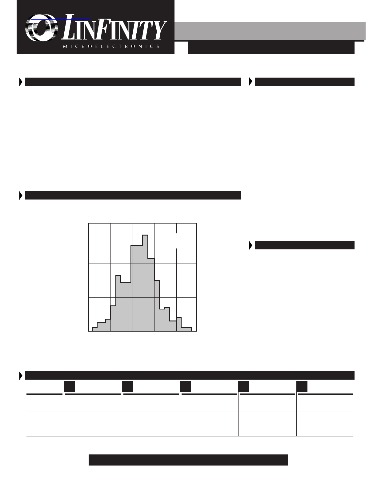
PRODUCT HIGHLIGHT
I NITIAL OSCILLATOR ACCURACY
15
10
Sample Size = 45
Sample Size = 279
Mean 411.887
Mean 401.661
Std. Dev. = 4.3
Std. Dev. = 3.8
N OT RECOMMENDED FOR NEW DESIGNS
KEY FEATURES
■■
■ IMPROVED REFERENCE INITIAL
■■
TOLERANCE (±1% max.)
■■
■ IMPROVED OSCILLATOR INITIAL
■■
ACCURACY (±3% typ.)
■■
■ IMPROVED STARTUP CURRENT
■■
(500µA typ.)
■■
■ PROP DELAY TO OUTPUTS (50ns typ.)
■■
p 10V TO 30V OPERATION
p 5.1V REFERENCE TRIMMED TO ±1%
p 2MHZ OSCILLATOR CAPABILITY
p 1.5A PEAK TOTEM-POLE DRIVERS
p U.V. LOCKOUT WITH HYSTERESIS
p NO OUTPUT DRIVER "FLOAT"
p PROGRAMMABLE SOFTSTART
p DOUBLE-PULSE SUPPRESSION LOGIC
p WIDEBAND LOW-IMPEDANCE ERROR
AMPLIFIER
p CURRENT-MODE OR VOLTAGE-MODE
CONTROL
p WIDE CHOICE OF HIGH-FREQUENCY
PACKAGES
HIGH RELIABILITY FEATURES
■■
■ AVAILABLE TO MIL-STD-883B
■■
■■
■ LINFINITY LEVEL "S" PROCESSING AVAIL.
■■
5
Percentage of Units - %
0
390 395 400 405 410
415
Initial Oscillator Accuracy - KHz
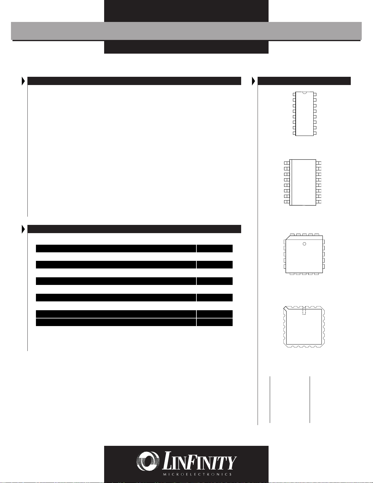
PACKAGE ORDER INFORMATION
T
(°C)
J
Plastic DIP
N
16-pin
0 to 70 SG3825CN SG3825CDW SG3825CQ SG3825CJ
-25 to 85 SG2825CN SG2825CDW SG2825CQ SG2825CJ
-55 to 125 SG1825CJ SG1825CL
MIL-STD-883 SG1825CJ/883B SG1825CL/883B
DESC SG1825CJ/DESC SG1825CL/DESC
Note: All surface-mount packages are available in Tape & Reel. Append the letter "T" to part number. (i.e. SG3825CDWT)
FOR FURTHER INFORMATION CALL (714) 898-8121
Copyright © 1994
Rev. 1.3 6/96
Plastic Wide SOIC
DW
16-pin
Plastic LCC
Q
20-pin
Ceramic DIP
J L
16-pin
11861 WESTERN AVENUE, GARDEN GROVE, CA. 92841
Ceramic LCC
20-pin
1
PRODUCT DATABOOK 1996/1997
SG1825C/SG2825C/SG3825C
H IGH-SPEED CURRENT-MODE PWM
OT RECOMMENDED FOR NEW DESIGNS
N
ABSOLUTE MAXIMUM RATINGS (Note 1)
Input Voltage (VIN and VC) .......................................................................................... 30V
Analog Inputs:
Error Amplifier and Ramp ........................................................................-0.3V to 7.0V
Softstart and I
Digital Input (Clock) .................................................................................... 1.5V to 6.0V
Driver Outputs ........................................................................................ -0.3V to V
Source / Sink Output Current (each output):
/S.D. ................................................................................ -0.3V to 6.0V
LIM
C
+1.5V
Continuous .............................................................................................................. 0.5A
Pulse, 500ns ............................................................................................................ 2.0A
Softstart Sink Current................................................................................................ 20mA
Clock Output Current ................................................................................................. 5mA
Error Amplifier Output Current ................................................................................. 5mA
Oscillator Charging Current ....................................................................................... 5mA
Operating Junction Temperature:
Hermetic (J, L Package) ....................................................................................... 150°C
Plastic (DW, N, Q Packages) ............................................................................... 150°C
Storage Temperature Range...................................................................... -65°C to 150°C
Lead Temperature (soldering, 10 seconds) ............................................................ 300°C
Note 1. Exceeding these ratings could cause damage to the device.
THERMAL DATA
N PACKAGE:
THERMAL RESISTANCE-JUNCTION TO AMBIENT,
DW PACKAGE:
THERMAL RESISTANCE-JUNCTION TO AMBIENT,
Q PACKAGE:
THERMAL RESISTANCE-JUNCTION TO AMBIENT,
J PACKAGE:
THERMAL RESISTANCE-JUNCTION TO AMBIENT,
L PACKAGE:
THERMAL RESISTANCE-JUNCTION TO CASE,
THERMAL RESISTANCE-JUNCTION TO AMBIENT,
Junction Temperature Calculation: TJ = TA + (P
The θ
numbers are guidelines for the thermal performance of the device/pc-board
JA
system. All of the above assume no ambient airflow.
θθ
θ
θθ
JA
θθ
θ
θθ
JA
θθ
θ
θθ
JA
θθ
θ
θθ
JA
θθ
θ
θθ
JC
θθ
θ
θθ
JA
x θ
).
D
JA
65°C/W
95°C/W
80°C/W
80°C/W
35°C/W
120°C/W
PACKAGE PIN OUTS
INV. INPUT
N.I. INPUT
E/A OUTPUT
CLOCK
SOFTSTART
INV. INPUT
N.I. INPUT
E/A OUTPUT
CLOCK
R
C
RAMP
SOFTSTART
418
616
814
1 16
215
314
413
512
R
T
611
C
T
710
RAMP
89
J & N PACKAGE
(Top View)
1 16
215
314
413
512
T
611
T
710
89
DW PACKAGE
(Top View)
321
4
5
6
7
8
911121310
Q PACKAGE
(Top View)
3212019
9 11121310
20 19
V
REF
+V
IN
OUTPUT B
V
C
PWR GND
OUTPUT A
GROUND
I
/ S.D.
LIM
+V
REF
+V
IN
OUTPUT B
V
C
PWR GND
OUTPUT A
GROUND
I
/ S.D.
LIM
18
17
16
15
14
175
157
L PACKAGE
(Top View)
1. N.C.
2. INV. INPUT
3. N.I. INPUT
4. E/A OUTPUT
5. CLOCK
6. N.C.
7. R
T
8. C
T
9. RAMP
10. SOFTSTART
2
11. N.C.
12. I
/ S.D.
LIM
13. GROUND
14. OUTPUT A
15. PWR GND
16. N.C.
17. V
C
18. OUTPUT B
19. +V
IN
20. V
REF
Copyright © 1994
Rev. 1.3 6/96
PRODUCT DATABOOK 1996/1997
H IGH-SPEED CURRENT-MODE PWM
N OT RECOMMENDED FOR NEW DESIGNS
RECOMMENDED OPERATING CONDITIONS (Note 2)
Parameter Symbol Units
Supply Voltage Range
Voltage Amp Common Mode Range
Ramp Input Voltage Range
Current Limit / Shutdown Voltage Range
Source / Sink Output Current
Continuous
Pulse, 500ns
Voltage Reference Output Current
Oscillator Frequency Range
Oscillator Charging Current
Oscillator Timing Resistor R
Oscillator Timing Capacitor C
Operating Ambient Temperature Range:
SG1825C T
SG2825C T
SG3825C T
Note 2. Range over which the device is functional.
SG1825C/SG2825C/SG3825C
Recommended Operating Conditions
Min. Typ. Max.
10 30 V
1.5 5.5 V
0 5.0 V
0 4.0 V
200 mA
1.0 A
110mA
4 1500 kHz
0.030 3 mA
T
T
A
A
A
1 100 kΩ
0.470 10 nF
070°C
-25 85 °C
-55 125 °C
ELECTRICAL CHARACTERISTICS (Note 3)
(Unless otherwise specified, these specifications apply over the operating ambient temperatures for SG3825C with 0°C ≤ TA ≤ 70°C, SG2825C with
-25°C ≤ TA ≤ 85°C, SG1825C with -55°C ≤ TA ≤ 125°C, and V
and case temperatures equal to the ambient temperature.)
Parameter
Symbol
=15V. Low duty cycle pulse testing techniques are used which maintains junction
IN=VC
Test Conditions
SG1825C/2825C
Min. Typ. Max. Min. Typ. Max.
SG3825C
Units
Reference Section
Output Voltage TJ = 25°C, IL = 1mA
Line Regulation VIN = 10 to 30V
Load Regulation IL = 1 to 10mA
Temperature Stability (Note 3) Over Operating Temperature
Total Output Range (Note 3) Over Line, Load, and Temperature
Output Noise Voltage (Note 3) f = 10Hz to 10kHz, IL = 0mA
Long Term Stability (Notes 3 &4) TJ = 125°C, t = 1000hrs
Short Circuit Current V
REF
= 0V
5.05 5.10 5.15 5.05 5.10 5.15 V
215 215 mV
515 515 mV
0.2 0.4 0.2 0.4 mV/°C
5.00 5.20 5.00 5.20 V
50 200 50 µV
525 525 mV
-15 -50 -100 -15 -50 -100 mA
RMS
Oscillator Section (Note 5)
Initial Accuracy TJ = 25°C, C
≤ 10pF
CLK
Voltage Stability VIN = 10 to 30V
Temperature Stability (Note 3) Over Rated Operating Temperature
Total Frequency Limits (Note 3) Over Line and Temperature
Minimum Frequency R
Maximum Frequency R
Clock High Level I
Clock Low Level I
= 100KΩ, C
T
= 1KΩ, C
T
= -1mA
CLK
= -1mA
CLK
= 0.01µF
T
= 470pF
T
Ramp Peak Voltage
Ramp Valley Voltage
Valley-to-Peak Amplitude
Note 3. This parameter is guaranteed by design and process control, but is not 100% tested in production.
Note 4. This parameter is non-accumulative, and represents the random fluctuation of the reference voltage within some error band when observed
over any 1000 hour period of time.
370 400 430 370 400 430 kHz
0.2 2 0.2 2 %
58 58 %
350 450 350 450 kHz
4 4 kHz
1.5 1.5 MHz
3.9 4.5 3.9 4.5 V
2.3 2.9 2.3 2.9 V
2.6 2.8 3.0 2.6 2.8 3.0 V
0.7 1.0 1.25 0.7 1.0 1.25 V
1.6 1.8 2.0 1.6 1.8 2.0 V
Copyright © 1994
Rev. 1.3 6/96
3
PRODUCT DATABOOK 1996/1997
SG1825C/SG2825C/SG3825C
H IGH-SPEED CURRENT-MODE PWM
OT RECOMMENDED FOR NEW DESIGNS
N
ELECTRICAL CHARACTERISTICS (Cont'd.)
Parameter
Symbol
Test Conditions
Error Amplifier Section (Note 6)
Input Offset Voltage R
Input Bias Current V
Input Offset Current V
DC Open Loop Gain A
Common Mode Rejection Over Rated Voltage Range, V
Power Supply Rejection VIN = 10V to 30V, V
Output Sink Current V
Output Source Current V
Output High Voltage I
Output Low Voltage I
Unity Gain Bandwidth (Note 3) A
Slew Rate (Note 3)
≤ 2KΩ, V
S
ERROR
ERROR
VOLVERROR
ERROR
ERROR
ERROR
ERROR
VOL
= 2.5V
= 2.5V
= 1 to 4V
= 1V
= 4V
= -0.5mA
= 1mA
= 0dB
ERROR
= 2.5V
ERROR
ERROR
= 2.5V
PWM Comparator Section (Note 5 & 7)
Ramp Input Bias Current
Minimum Duty Cycle V
Maximum Duty Cycle (Note 8) V
ERROR
ERROR
= 1V
= 4V
Zero Duty Cycle Threshold
Delay to Driver Output (Note 3) V
= 0V to 2V, V
RAMP
ERROR
= 2V
Softstart Section
CSS Charge Current V
CSS Discharge Current V
SOFTSTART
SOFTSTART
= 0.5V
= 1.0V
Current Limit / Shutdown Section (Note 9)
I
Input Bias Current
LIM
Current Limit Threshold
Shutdown Threshold
Delay to Driver Output (Note 3) V
SHUTDOWN
= 0V to 1.2V
Output Drivers Section (each output)
Output Low Level I
Output High Level I
VC Standby Current VC = 30V
Output Rise / Fall Time (Note 3) CL = 1000pF
= 20mA
SINK
I
= 200mA
SINK
SOURCE
I
SOURCE
= 20mA
= 200mA
Undervoltage Lockout Section
Start Threshold Voltage
UV Lockout Hysteresis
Supply Current Section (Note 5)
Start Up Current VIN = 8V
Operating Current V
Note 5. F
Note 6. VCM = 1.5V to 5.5V.
Note 7. V
Note 8. 100% duty cycle is defined as a pulsewidth equal to one oscillator period.
Note 9. V(I
= 400kHz (R
OSC
= 0V, unless otherwise specified.
RAMP
/S.D.) = 0V to 4.0V, unless otherwise specified.
LIM
= 3.65kΩ, C
T
= 1.0nF).
T
, V
, V(I
INV
RAMP
/S.D.) = 0V, V
LIM
N.I.
= 2.5V
= 1V
SG1825C/2825C
Min. Typ. Max. Min. Typ. Max.
SG3825C
Units
15 15 mV
0.6 3 0.6 3 µA
0.1 1 0.1 1 µA
60 95 60 95 dB
75 95 75 95 dB
85 110 85 110 dB
1 2.5 1 2.5 mA
-0.5 -1.3 -0.5 -1.3 mA
4.0 4.7 5.0 4.0 4.7 5.0 V
0 0.5 1.0 0 0.5 1.0 V
3 5.5 3 5.5 MHz
6 6 V/µsec
-1 -5 -1 -5 µA
00%
85 85 %
1.1 1.25 1.1 1.25 V
50 80 50 80 ns
39203920 µA
11 mA
±15 ±10 µA
0.9 1.0 1.1 0.9 1.0 1.1 V
1.25 1.40 1.55 1.20 1.40 1.55 V
50 80 50 80 ns
0.25 0.40 0.25 0.40 V
1.2 2.0 1.2 2.0 V
13.0 13.5 13.0 13.5 V
12.0 13.0 12.0 13.0 V
150 500 150 500 µA
30 60 30 60 ns
8.8 9.2 9.7 8.8 9.2 9.7 V
0.4 0.8 1.2 0.4 0.8 1.2 V
0.5 1.2 0.5 1.2 mA
22 33 22 33 mA
4
Copyright © 1994
Rev. 1.3 6/96

+V
D
GND
CLOCK
RAMP
PRODUCT DATABOOK 1996/1997
SG1825C/SG2825C/SG3825C
H IGH-SPEED CURRENT-MODE PWM
N OT RECOMMENDED FOR NEW DESIGNS
BLOCK DIAGRAM
V
REF
+9V
15
IN
10
4
R
5
T
C
6
T
1.25V
7
REFERENCE
REGULATOR
OSCILLATOR
16
+ 4.0V
Q
T
Q
S
RQ
V
13
11
OUTPUT A
OUTPUT B
14
POWER GN
12
C
E/A OUTPUT
N.I. INPUT
INV. INPUT
SOFTSTART
3
2
ERROR
1
8
FIGURE INDEX
Application Circuits
FIGURE #
1. HIGH-SPEED LAYOUT AND BYPASSING
2. MICROPOWER STARTUP
3. SOFTSTART FAST RESET
4. OSCILLATOR SYCHRONIZATION
5. OSCILLATOR FUNCTIONAL DIAGRAM
6. VOLTAGE AMPLIFIER CONNECTIONS
7. DRIVING SHIELDED CABLE
9µA
+ 1.0V
+ 1.4V
9
I
/S.D.
LIM
Copyright © 1994
Rev. 1.3 6/96
5

PRODUCT DATABOOK 1996/1997
C
T
R
T
10
12
6
PWR GND
GND
+V
IN
15
0.1µF
+ V
IN
5
SG1825C
CLK
4
C
T
R
T
10
12
6
PWR GND
GND
+V
IN
15
0.1µF
5
SG1825C
V
REF
16
CLK
4
C
T
R
T
MASTER SLAVE
+
V
C
C
SS
10
12
13
PWR GND
GND
+V
IN
15
0.1µF
+ V
IN
1µF
8
SG1825C
R
1
100W
C
SOFTSTART
SG1825C/SG2825C/SG3825C
H IGH-SPEED CURRENT-MODE PWM
OT RECOMMENDED FOR NEW DESIGNS
N
APPLICATION INFORMATION
HIGH-SPEED LAYOUT AND BYPASSING
The SG1825C, like all high-speed circuits, requires extra attention to external
conductor and component layout to minimize undesired inductive and
capacitive effects. All lead lengths must be as short as possible. The best
printed circuit board choice would be a four-layer design, with the two
internal planes supplying power and ground. Signal interconnects should
be placed on the outside, giving a conductor-over-ground-plane
(microstrip) configuration. A two-sided printed circuit board with one side
dedicated as a ground plane is next best, and requires careful component
placement by a skilled pc designer.
Two supply bypass capacitors should be employed: a low-inductance
0.1µF ceramic within 0.25 inches of the +VIN pin for high frequencies, and
a 1 to 5µF solid tantalum within 0.5 inches of the V
reservoir for the high-peak output currents. A low-inductance .01µF bypass
pin to provide an energy
C
for the reference output is also recommended.
MICROPOWER STARTUP
Since the SG1825C typically draws 700µA of supply current before turning
on, a low power bleeder resistor from the rectified AC line supply is all that
is required for startup. A start capacitor, C
current from the bleeder resistor. When the turn-on threshold voltage is
, is charged with the excess
S
reached, the PWM circuit becomes active, energizing the power transistors.
The additional operating current required by the PWM is then provided by
a bootstrap winding on the main high-frequency power transformer.
APPLICATION FIGURES
FIGURE 1. HIGH-SPEED LAYOUT and BYPASSING
16
V
REF
L1
GND
L2
SG1825C
15
+V
0.1µF
V
IN
FIGURE 2. MICROPOWER STARTUP
240
120
R
PWR GND
GND
IN
B
C
S
+ V
13
V
C
12
10
1µF
15
0.1µF
IN
V
REF
0.01µF
TO POWER TRANSFORMER
SG1825C
13
V
C
POWER
12
GND
10
GND
+V
IN
1µF
SOFTSTART CIRCUIT / OUTPUT DUTY CYCLE LIMIT
The softstart pin of the SG1825C is held low when either the chip is in the
FIGURE 3. SOFTSTART FAST RESET
micropower mode, or when a voltage greater than +1.4 volts is present at
the I
is clamped to the Softstart pin voltage, providing a ramp-up of peak charging
pin. The maximum positive swing of the voltage error amplifier
LIM/S.D.
currents in the power semiconductors at turn-on.
In some cases, the duration of the Shutdown signal can be too short to
fully discharge the softstart capacitor. The illustrated resistor/discrete PNP
transistor configuration can be used to shorten the discharge time by a factor
of 50 or more. When the internal discharge transistor in the SG1825C turns
on, current will flow through surge limit resistor R1. As the resistor drop
approaches 0.6 volts, the external PNP turns on, providing a low resistance
discharge path for the energy in the softstart capacitor. The capacitor will
be rapidly discharged to +0.7 volts, which corresponds to zero duty cycle
in the pulse width modulator.
FREQUENCY SYNCHRONIZATION
FIGURE 4. OSCILLATOR SYCHRONIZATION
Two or three SG1825C oscillators may be locked together with the
interconnection scheme shown, if the devices are within an inch or so of
each other. A master unit is programmed for desired frequency with R
as usual. The oscillators in the slave units are disabled by grounding C
C
T
and by connecting RT to V
clock of the master with the wire-OR connection shown.
. The logic in the slave units is locked to the
REF
and
T
T
Many SG1825Cs can be locked to a master system clock by wiring the
oscillators as slave units, and distributing the master clock to each using a
tree-fanout geometry.
6
Copyright © 1994
Rev. 1.3 6/96

PRODUCT DATABOOK 1996/1997
V
V
V
REF
2
1
3
R
3
RZC
P
R
4
POSITIVE
OUTPUT
VOLTAGE
V
REF
2
1
3
R
3
RZC
P
V
REF
2
V
ERROR
V
ERROR
FIGURE B
FIGURE A
R
1
R
2
R
1
R
2
NEGATIVE
OUTPUT
VOLTAGE
R
4
SG1825C/SG2825C/SG3825C
H IGH-SPEED CURRENT-MODE PWM
N OT RECOMMENDED FOR NEW DESIGNS
APPLICATION INFORMATION
OSCILLATOR
The oscillator frequency is programmed by external timing components R
T
and CT. A nominal +3.0 volts appears at the RT pin. The current flowing
through R
current to flow out the C
a linear ramp. When the upper threshold of +2.8 volts is reached, a
is mirrored internally with a 1:1 ratio. This causes an identical
T
pin, charging the timing capacitor and generating
T
discharge network reduces the ramp voltage to +1.0, where a new charge
cycle begins.
The Clock output pin is LOW (+2.3 volts) during the charge cycle, and
HIGH (+4.5 volts) during the discharge cycle. The Clock pin is driven by
an NPN emitter follower, and so can be wire-ORed. Each Clock pin can drive
a 1mA load. Since the internal current-source pulldown is approximately
400µA, the DC fan-out to other SG1825C Clock pins is at least two.
The type of capacitor selected for C
frequencies, non-ideal characteristics such as effective series resistance
is very important. At high
T
(ESR), effective series inductance (ESL), dielectric loss and dielectric
absorption all affect frequency accuracy and stability. RF capacitors such as
silver mica, glass, polystrene, or COG ceramics are recommended. Avoid
high-K ceramics, which work best in DC bypass applications.
ERROR AMPLIFIER
The voltage error amplifier is a true operational amplifier with lowimpedance output, and can be gain-stabilized using conventional feedback
techniques. The typical DC open-loop gain is 95dB, with a single lowfrequency pole at 100Hz.
The input connections to the error amplifier are determined by the
polarity of the power supply output voltage. For positive supplies, the
common-mode voltage is +5.1 volts and the feedback connections in Figure
A are used. With negative outputs, the common-mode voltage is half the
reference, and the feedback divider is connected between the negative
output and the +5.1 volt reference as shown in Figure B.
APPLICATION FIGURES
FIGURE 5. OSCILLATOR FUNCTIONAL DIAGRAM
3V
I
R
R
T
5
IC = I
C
T
6
R
2.8V 1.0V
FIGURE 6. VOLTAGE AMPLIFIER CONNECTIONS
SG1825C
+ 5.1V
4
400µA
CLOCK
+ 4.5
+ 2.3
OUTPUT DRIVER
The output drivers are designed to provide up to 1.5 Amps peak output
current. To minimize ringing on the output waveform, which can be
destructive to both the power MOSFET and the PWM chip, the series
FIGURE 7. DRIVING SHIELDED CABLE
inductance seen by the drivers should be as low as possible.
One solution is to keep the distance between the PWM and MOSFET gate
as short as possible, and to use carbon composition series damping resistors.
SG1825C
13
V
C
FARADAY SHIELD
A Faraday shield to intercept radiated EMI from the power transistors is
usually required with its choice.
A second approach is to place the MOSFETs some distance from the PWM
chip, and use a series-terminated transmission line to preserve drive pulse
W
11
24
*
50W
50W
fidelity. This will minimize noise radiated back to the sensitive analog
circuitry of the SG1825C. A Faraday shield may also be required.
If the drivers are connected to an isolation transformer, or if kickback
through C
peak Schottky diodes will limit undershoot to less than -0.3 volts.
Copyright © 1994
Rev. 1.3 6/96
of the MOSFET is severe, clamp diodes may be required. 1 Amp
GD
PWR GND
12
GND
10
* SCHOTTKY CLAMP MAY BE REQUIRED
7
 Loading...