

查询JAN1524J供应商
SG1524/SG2524/SG3524
REGULATING PULSE WIDTH MODULATOR
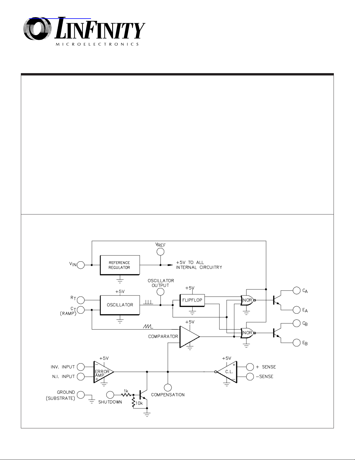
DESCRIPTION
This monolithic integrated circuit contains all the control circuitry for a
regulating power supply inverter or switching regulator. Included in a 16pin dual-in-line package is the voltage reference, error amplifier, oscillator,
pulse width modulator, pulse steering flip-flop, dual alternating output
switches and current limiting and shut-down circuitry. This device can be
used for switching regulators of either polarity, transformer coupled DC to
DC converters, transformerless voltage doublers and polarity converters,
as well as other power applications. The SG1524 is specified for operation
over the full military ambient temperature range of -55°C to +125°C, the
SG2524 for -25°C to +85°C, and the SG3524 is designed for commercial
applications of 0°C to +70°C.
BLOCK DIAGRAM
FEATURES
••
• 8V to 40V operation
••
••
• 5V reference
••
••
• Reference line and load regulation of 0.4%
••
••
• Reference temperature coefficient < ± 1%
••
••
• 100Hz to 300KHz oscillator range
••
••
• Excellent external sync capability
••
••
• Dual 50mA output transistors
••
••
• Current limit circuitry
••
••
• Complete PWM power control circuitry
••
••
• Single ended or push-pull outputs
••
••
• Total supply current less than 10mA
••
HIGH RELIABILITY FEATURES - SG1524
♦♦
♦ Available to MIL-STD-883B and DESC SMD
♦♦
♦♦
♦ MIL-M-38510/12601BEA - JAN1524J
♦♦
♦♦
♦ Radiation data available
♦♦
♦♦
♦ LMI level "S" processing available
♦♦
4/90 Rev 1.1 2/94 LINFINITY Microelectronics Inc.
Copyright 1994 11861 Western Avenue
1 (714) 898-8121
∞ ∞
∞ Garden Grove, CA 92841
∞ ∞
∞∞
∞ FAX: (714) 893-2570
∞∞
ABSOLUTE MAXIMUM RATINGS (Note 1)
Input Voltage (+VIN)............................................................. 42V
Collector Voltage ................................................................ 40V
Logic Inputs...........................................................-0.3V to 5.5V
Current Limit Sense Inputs ...................................-0.3V to 0.3V
Output Current (each transistor) .................................... 100mA
Reference Load Current .................................................. 50mA
Note 1. Values beyond which damage may occur.
THERMAL DATA
J Package:
Thermal ResistanceThermal Resistance-
N Package:
Thermal ResistanceThermal Resistance-
D Package:
Thermal ResistanceThermal Resistance-
L Package:
Thermal ResistanceThermal Resistance-
Junction to Case, θ
Junction to Ambient, θ
Junction to Case, θ
Junction to Ambient, θ
Junction to Case, θ
Junction to Ambient, θ
Junction to Case, θ
Junction to Ambient, θ
.................. 30°C/W
JC
.............. 80°C/W
JA
.................. 40°C/W
JC
............. 65°C/W
JA
................... 50°C/W
JC
............ 120°C/W
JA
.................. 35°C/W
JC
........... 120°C/W
JA
SG1524/SG2524/SG3524
Oscillator Charging Current ................................................5mA
Operating Junction Temperature
Hermetic (J, L Packages) .............................................150°C
Plastic (N, D Packages) ............................................... 150°C
Storage Temperature Range .............................-65°C to 150°C
Lead Temperature (Soldering, 10 seconds) ....................300°C
Note A. Junction Temperature Calculation: TJ = TA + (PD x θJA).
Note B. The above numbers for
thermal resistance of the package in a standard mounting configuration. The θ
guidelines for the thermal performance of the device/pcboard system. All of the above assume no ambient
airflow.
θJC are maximums for the limiting
numbers are meant to be
JA
RECOMMENDED OPERATING CONDITIONS (Note 2)
Input Voltage (+VIN) ...................................................
Collector Voltage .......................................................
Error Amp Common Mode Range ..........................
Current Limit Sense Common Mode Range ........
Output Current (each transistor) ...............................
Reference Load Current ...........................................
Oscillator Charging Current ..................................
Note 2: Range over which the device is functional and parameter limits are guaranteed.
8V to 40V
0V to 40V
1.8V to 3.4V
-0.3V to 0.3V
0 to 50mA
0 to 20mA
30µA to 2mA
Oscillator Frequency Range .........................
Oscillator Timing Resistor (R
Oscillator Timing Capacitor (C
Operating Ambient Temperature Range
SG1524 .........................................................
SG2524 ...........................................................
SG3524 ...............................................................
) ........................
T
) ............................
T
100Hz to 300KHz
1.8KΩ to 100KΩ
1nF to 1.0µF
-55°C to 125°C
-25°C to 85°C
0°C to 70°C
ELECTRICAL CHARACTERISTICS
(Unless otherwise specified, these specifications apply over the operating ambient temperatures for SG1524 with -55° C ≤ TA ≤ 125°C, SG2524 with
-25°C ≤ T
case temperatures equal to the ambient temperature.)
Reference Section
Output Voltage
Line Regulation
Load Regulation
Temperature Stability
Total Output Voltage Range (Note 7)
Short Circuit Current
Note 3. I
≤ 85°C, SG3524 with 0°C ≤ TA ≤ 70°C, and +VIN = 20V. Low duty cycle pulse testing techniques are used which maintains junction and
A
= 0mA
L
(Note 3)
(Note 7)
TJ = 25°C
= 8V to 40V
V
IN
I
= 0 to 20mA
L
Over Operating Temperature Range
Over Line, Load and Temperature
V
= 0V
REF
Min. Typ. Max.
5.00
4.80
5.20
20
50
50
4.80
25
50
5.20
150
SG3524SG1524/2524
Min. Typ. Max.
4.60
5.00505.40
4.60
25
30
50
50
5.40
150
UnitsTest ConditionsParameter
V
mV
mV
mV
V
mA
4/90 Rev 1.1 2/94 LINFINITY Microelectronics Inc.
Copyright 1994 11861 Western Avenue
2 (714) 898-8121
∞ ∞
∞ Garden Grove, CA 92841
∞ ∞
∞∞
∞ FAX: (714) 893-2570
∞∞

ELECTRICAL CHARACTERISTICS (continued)
SG1524/SG2524/SG3524
Oscillator Section
Initial Accuracy
(Note 4)
TJ = 25°C
MIN ≤ T
V
Voltage Stability
Maximum Frequency
Sawtooth Peak Voltage
Sawtooth Valley Voltage
Clock Amplitude
= 8V to 40V
IN
= 2KΩ, CT = 1nF
R
T
V
= 40V
IN
V
= 8V
IN
Clock Pulse Width
Error Amplifier Section (Note 5)
Input Offset Voltage
RS ≤ 2KΩ
Input Bias Current
Input Offset Current
DC Open Loop Gain
Output Low Level
Output High Level
Common Mode Rejection
Supply Voltage Rejection
Gain-Bandwidth Product
P.W.M. Comparator
(Note 7)
(Note 4)
Minimum Duty Cycle
Maximum Duty Cycle
Current Limit Amplifier Section
Sense Voltage
R
≥10MΩ, TJ = 25°C
L
- V
V
PIN 1
V
- V
PIN 2
V
= 1.8V to 3.4V
CM
= 8V to 40V
V
IN
T
= 25°C
J
V
= 0.5V
COMP
V
= 3.6V
COMP
(Note 6)
TJ = 25°C
Input Bias Current
Shutdown Section
Threshold Voltage TJ = 25°C
MIN ≤ T
Output Section (each transistor)
Collector Leakage Current
Collector Saturation Voltage
Emitter Output Voltage
Collector Voltage Rise Time
Collector Voltage Fall Time
VCE = 40V
I
= 50mA
C
= 50mA
I
E
R
= 2KΩ
C
R
= 2KΩ
C
Power Consumption
VIN = 40VStandby Current
≤ MAX
J
≥ 150mV
PIN 2
≥150mV
PIN 1
≤ MAX
J
SG1524/2524 SG3524
Min. Typ. Max.
36
40
34
0.1
200
400
3
0.6
1
3.2
0.3
0.5
1
Min. Typ. Max.
36
44
34
46
1
200
3
3.8
0.6
1.2
3.2
0.3
1.5
5
10
0.1
400
1
0.5
60
3.8
0.2
4.2
72
3.8
0.2
4.2
70
55
2
1
1
0
49
200190
45 4945
210
180 200 220
200
0.80.5
1.2
0.5
0.8 1.2
0.2
1.8
0.2
50
2
1717
0.4
0.2
UnitsTest ConditionsParameter
KHz
44
40
KHz
46
%
1
KHz
3.8
1.2
1
V
V
V
µs
1.5
mV
10
2
µA
10
1
µA
2
dB
0.5
V
V
dB
dB
2
MHz
0
%
%
200mVµA
1.8VV
µA
50
V
2
V
µs
0.4
µs
0.2
107107mA
Note 4. F
Note 5. V
Note 6. V
Note 7. These parameters, although guaranteed over the recommended operating conditions, are not 100% tested in production.
4/90 Rev 1.1 2/94 LINFINITY Microelectronics Inc.
Copyright 1994 11861 Western Avenue
= 40KHz (RT = 2.9KΩ, CT = .01µF)
OSC
= 2.5V
CM
= 0V
CM
∞ ∞
∞ Garden Grove, CA 92841
3 (714) 898-8121
∞ ∞
∞∞
∞ FAX: (714) 893-2570
∞∞

APPLICATION NOTES
OSCILLATOR
The oscillator in the SG1524 uses an external resistor RT to
establish a constant charging current into an external capacitor
. While this uses more current than a series-connected RC, it
C
T
provides a linear ramp voltage at C
dependent reference for the PWM comparator. The charging
current is equal to 3.6V/R
30µA and 2mA. The equivalent range for R
, and should be restricted to between
T
which is used as a time-
T
is 1.8K to 100K.
T
SG1524/SG2524/SG3524
Note that for buck regulator topologies, the two outputs can be
wire-ORed for an effective 0-90% duty cycle range. With this
connection, the output frequency is the same as the oscillator
frequency. For push-pull applications, the outputs are used
separately; the flip-flop limits the duty cycle range at each output
to 0-45%, and the effective switching frequency at the transformer is 1/2 the oscillator frequency.
The range of values for C
determines the pulse width of the oscillator output pulse.
of C
T
The pulse is used (among other things) as a blanking pulse to
also has limits, as the discharge time
T
both outputs to insure that there is no possibility of having both
outputs on simultaneously during transitions. This output
deadtime relationship is shown in Figure 1. A pulse width below
0.35 microseconds may cause failure of the internal flip-flop to
toggle. This restricts the minimum value of C
Although the oscillator output is a convenient oscilloscope sync
to 1000pF. (Note:
T
input, the probe capacitance will increase the pulse width and
decrease the oscillator frequency slightly.) Obviously, the upper
limit to the pulse width is determined by the modulation range
required in the power supply at the chosen switching frequency.
Practical values of C
successful 120 Hz oscillators have been implemented with val-
fall between 1000pF and 0.1µF, although
T
ues up to 5µF and a series surge limit resistor of 100 ohms.
The oscillator frequency is approximately 1/R
ohms, C is in microfarads, and the frequency is in Megahertz. For
; where R is in
T•CT
greater accuracy, the chart in Figure 2 may be used for a wide
range of operating frequencies.
If it is desired to synchronize the SG1524 to an external clock, a
positive pulse may be applied to the clock pin. The oscillator
should be programmed with RT and CT values that cause it to freerun at 90% of the external sync frequency. A sync pulse with a
maximum logic 0 of +0.3 volts and a minimum logic 1 of +2.4 volts
applied to Pin 3 will lock the oscillator to the external source. The
minimum sync pulsewidth should be 200 nanoseconds, and the
maximum is determined by the required deadtime. The clock pin
should never be driven more negative than -0.3 volts, nor more
positive than +5.0 volts. The nominal resistance to ground is
3.2K at the clock pin, ±25% over temperature.
If two or more SG1524s must be synchronized together, program
one master unit with R
pins on the slaves open, connect the CT pins to the CT of
the R
T
the master, and connect the clock pins to the clock pin of the
master. Since C
works best when all devices are close together.
and CT for the desired frequency. Leave
T
is a high-impedance node, this sync technique
T
FIGURE 1 - OUTPUT STAGE DEADTIME VS. C
4/90 Rev 1.1 2/94 LINFINITY Microelectronics Inc.
Copyright 1994 11861 Western Avenue
T
4 (714) 898-8121
FIGURE 2 - OSCILLATOR FREQUENCY VS. RT AND C
∞ ∞
∞ Garden Grove, CA 92841
∞ ∞
T
∞∞
∞ FAX: (714) 893-2570
∞∞

APPLICATION NOTES (continued)
SG1524/SG2524/SG3524
CURRENT LIMITING
The current limiting circuitry of the SG1524 is shown in Figure 3.
By matching the base-emitter voltages of Q1 and Q2, and
assuming a negligible voltage drop across R1:
C.L. Threshold = VBE(Q1) + I1• R2 - VBE(Q2) = I1• R
~ 200 mV
2
Although this circuit provides a relatively small threshold with a
negligible temperature coefficient, there are some limitations to
its use because of its simplicity.
The most important of these is the limited common-mode voltage
range: ±0.3 volts around ground. This requires sensing in the
ground or return line of the power supply. Also precautions
should be taken to not turn on the parasitic substrate diode of the
integrated circuit, even under transient conditions. A Schottky
clamp diode at Pin 5 may be required in some configurations to
achieve this.
A second factor to consider is that the response time is relatively
slow. The current limit amplifier is internally compensated by R
, C
and Q1, resulting in a roll-off pole at approximately 300 Hz.
1 ,
A third factor to consider is the bias current of the C.L. Sense
1
pins. A constant current of approximately 150µA flows out of Pin
4, and a variable current with a range of 0-150µA flows out of Pin
5. As a result, the equivalent source impedance seen by the
current sense pins should be less than 50 ohms to keep the
threshold error less than 5%.
Since the gain of this circuit is relatively low (42 dB), there is a
transition region as the current limit amplifier takes over pulse
width control from the error amplifier. For testing purposes,
threshold is defined as the input voltage required to get 25% duty
cycle (+2 volts at the error amplifier output) with the error amplifier
signaling maximum duty cycle.
APPLICATION NOTE: If the current limit function is not used on
the SG1524, the common-mode voltage range restriction requires both current sense pins to be grounded.
FIGURE 3 - CURRENT LIMITING CIRCUITRY OF THE SG1524
Push-pull outputs are used in this transformer-coupled DC-DC
In this conventional single-ended regulator circuit, the two outputs of the SG1524 are connected in parallel for effective 0 - 90%
duty-cycle modulation. The use of an output inductor requires
and R-C phase compensation network for loop stability.
regulating converter. Note that the oscillator must be set at twice
the desired output frequency as the SG1524's internal flip-flop
divides the frequency by 2 as it switches the P.W.M. signal from
one output to the other. Current limiting is done here in the
primary so that the pulse width will be reduced should transformer
saturation occur.
4/90 Rev 1.1 2/94 LINFINITY Microelectronics Inc.
Copyright 1994 11861 Western Avenue
5 (714) 898-8121
∞ ∞
∞ Garden Grove, CA 92841
∞ ∞
∞∞
∞ FAX: (714) 893-2570
∞∞

CONNECTION DIAGRAMS & ORDERING INFORMATION (See Notes Below)
SG1524/SG2524/SG3524
16-PIN CERAMIC DIP
J - PACKAGE
16-PIN PLASTIC DIP
N - PACKAGE
16-PIN NARROW BODY
PLASTIC S.O.I.C.
D - PACKAGE
20-PIN CERAMIC
LEADLESS CHIP CARRIER
L- PACKAGE
Part No.Package
Ambient
Temperature Range
SG1524J/883B -55°C to 125°C
JAN1524J -55°C to 125°C
SG1524J/DESC -55°C to 125°C
SG1524J -55°C to 125°C
SG2524J -25°C to 85°C
SG3524J 0°C to 70°C
SG2524N -25°C to 85°C
SG3524N 0°C to 70°C
SG2524D -25°C to 85°C
SG3524D 0°C to 70°C
SG1524L/883B -55°C to 125°C
SG1524L -55°C to 125°C
Connection Diagram
INV. INPUT
N.I. INPUT
OSC. OUTPUT
+C.L. SENSE
-C.L. SENSE
R
T
C
T
INV. INPUT
N.I. INPUT
OSC. OUTPUT
+C.L. SENSE
-C.L. SENSE
R
T
C
T
GROUND
1. N.C.
2. V
REF
3. INV. INPUT
4. N.I. INPUT
5. OSC. OUTPUT
6. + C.L. SENSE
7. - C.L. SENSE
8. R
T
9. C
T
10. GROUND
321
4
5
6
7
8
9 11121310
11516
2
3
4
5
6
7
8
1
2
3
4
5
6
7
8
14
13
12
11
10
9
16
15
14
13
12
11
10
9
20 19
V
REF
+V
IN
E
B
C
B
C
A
E
A
SHUTDOWN
COMPENSATIONGROUND
V
REF
+V
IN
E
B
C
B
C
A
E
A
SHUTDOWN
COMPENSATION
11. COMP
12. SHUTDOWN
18
13. N.C.
14. E
17
15. C
16
16. N.C.
15
17. C
14
18. E
19. N.C.
20. +V
A
A
B
B
IN
Note 1. Contact factory for JAN and DESC product availablity.
2. All packages are viewed from the top.
4/90 Rev 1.1 2/94 LINFINITY Microelectronics Inc.
Copyright 1994 11861 Western Avenue
6 (714) 898-8121
∞ ∞
∞ Garden Grove, CA 92841
∞ ∞
∞∞
∞ FAX: (714) 893-2570
∞∞
 Loading...