

DESCRIPTION
The SG117A Series are 3-terminal positive adjustable voltage
regulators which offer improved performance over the original 117
design. A major feature of the SG117A is reference voltage
tolerance guaranteed within ± 1%, allowing an overall power supply
tolerance to be better than 3% using inexpensive 1% resistors. Line
and load regulation performance has been improved as well.
Additionally, the SG117A reference voltage is guaranteed not to
exceed 2% when operating over the full load, line and power
dissipation conditions. The SG117A adjustable regulators offer an
improved solution for all positive voltage regulator requirements
with load currents up to 1.5A.
FEATURES
••
••
• 1% output voltage tolerance
••
••
• 0.01%/V line regulation
••
••
• 0.3% load regulation
••
••
• Min. 1.5A output current
••
••
• Available in hermetic TO-220
HIGH RELIABILITY FEATURES-SG117A/SG117
♦♦
♦♦
♦ Available to MIL-STD-883 and DESC SMD
♦♦
♦♦
♦ MIL-M38510/11704BYA - JAN117K
♦♦
♦♦
♦ MIL-M38510/11703BXA - JAN117T
♦♦
♦♦
♦ LMI level "S" processing available
SG117A/SG217A/SG317A
SG117/SG217/SG317
1.5 AMP THREE TERMINAL
ADJUSTABLE VOLTAGE REGULATOR
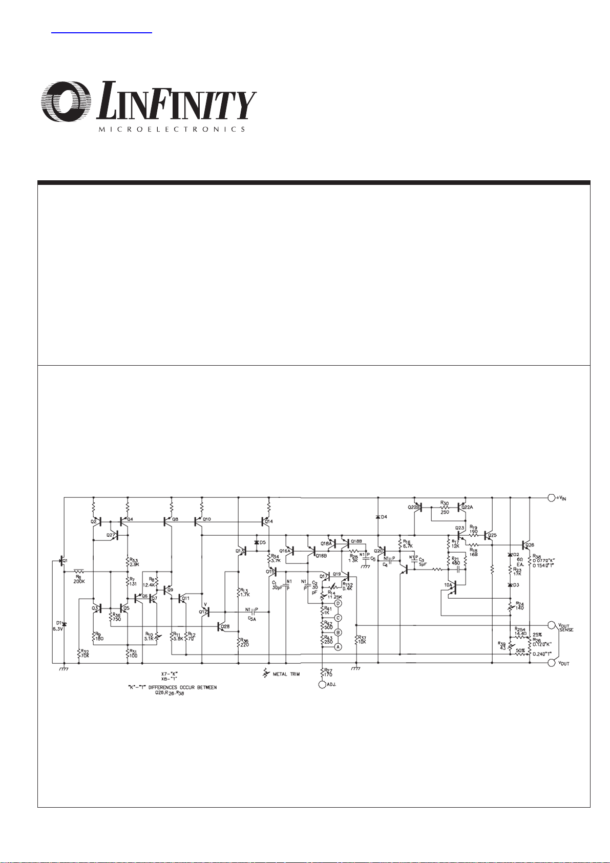
SCHEMATIC DIAGRAM
2/93 Rev 1.2 10/02 LINFINITY Microelectronics Inc.
Copyright 1994 11861 Western Avenue
∞ ∞
∞ ∞
∞ Garden Grove, CA 92841
1 (714) 898-8121
∞∞
∞∞
∞ FAX: (714) 893-2570
查询SG217R供应商
SG117A/SG117 SERIES
2/93 Rev 1.2 10/02 LINFINITY Microelectronics Inc.
Copyright 1994 11861 Western Avenue
∞ ∞
∞ ∞
∞ Garden Grove, CA 92841
2 (714) 898-8121
∞∞
∞∞
∞ FAX: (714) 893-2570
ELECTRICAL CHARACTERISTICS
(Unless otherwise specified, these specifications apply over full operating ambient temperatures for SG117A/SG117 with -55°C ≤ TA ≤ 125°C, SG217A/
SG217 with -25°C ≤ TA ≤ 150°C, SG 317A/SG317 with 0°C ≤ TA ≤ 125°C, VIN - V
OUT
= 5.0V , and for I
OUT
= 500mA (K, R, and IG), and I
OUT
= 100mA
(T and L packages). Although power dissipation is internally limited, these specifications are applicable for power dissipations of 2W for the T and L
packages, and 20W for the K, R, and IG packages. I
MAX
is 1.5A for the K, R, and IG packages and 500mA for the T and L packages. Low duty cycle
pulse testing techniques are used which maintains junction and case temperatures equal to the ambient temperature.)
Power Dissipation ........................................
Input to Output Voltage Differential .................................
Storage Temperature Range ..........................
ABSOLUTE MAXIMUM RATINGS (Note 1)
Internally Limited
40V
-65°C to 150°C
Operating Junction Temperature
Hermetic (K, R, T, L, IG-Packages) ............................
Lead Temperature (Soldering, 10 Seconds) ..............
150°C
300°C
Note 1. Exceeding these ratings could cause damage to the device.
Input Voltage Range .............................. (V
OUT
+ 3.5V) to 37V Operating Junction Temperature Range
SG117A/SG117 .........................................
SG217A/SG217 .........................................
SG317A/SG317 ............................................
-55°C to 150°C
-25°C to 150°C
0°C to 125°C
Note 2. Range over which the device is functional.
Note 3. These ratings are applicable for junction temperatures of less than 150°C.
RECOMMENDED OPERATING CONDITIONS (Note 2 & 3)
Units
SG117/SG217
Min. Typ. Max.Min. Typ. Max.
SG117A/SG217A
Parameter Test Conditions
I
OUT
= 10mA TA = 25°C
3V ≤ (V
IN
- V
OUT
) ≤ 40V, P ≤ P
MAX
,
10mA ≤ I
OUT
≤ I
MAX
3V ≤ (VIN - V
OUT
) ≤ 40V, IL = 10mA
T
A
= 25°C
T
A
= T
MIN
to T
MAX
10mA ≤ I
OUT
≤ I
MAX
V
OUT
≤ 5V, TA = 25°C
V
OUT
≥ 5V, TA = 25°C
V
OUT
≤ 5V
V
OUT
≥ 5V
T
A
= 25°C, 20ms pulse
V
OUT
= 10V, f =120Hz
C
ADJ
= 1µF, TA = 25°C
C
ADJ
= 10µF
10mA ≤ I
OUT
≤ I
MAX
, 2.5V ≤ (VIN - V
OUT
) ≤ 40V
1.238
1.225
66
1.250
1.250
0.005
0.01
5
0.1
20
0.3
0.002
65
80
50
0.2
1.262
1.270
0.01
0.02
15
0.3
50
1
0.02
100
5
1.20661.25
0.01
0.02
5
0.1
20
0.3
0.03
65
80
50
0.2
1.30
0.02
0.05
15
0.3
50
1
0.07
100
5
V
V
%/V
%/V
mV
%
mV
%
%/W
dB
dB
µA
µA
K Package:
Thermal Resistance-
Junction to Case, θ
JC
................. 3.0°C/W
Thermal Resistance-
Junction to Ambient, θ
JA
.............. 35°C/W
R Package:
Thermal Resistance-
Junction to Case, θ
JC
................. 5.0°C/W
Thermal Resistance-
Junction to Ambient, θ
JA
............. 40°C/W
T Package:
Thermal Resistance-
Junction to Case, θ
JC
.................. 15°C/W
Thermal Resistance-
Junction to Ambient, θ
JA
........... 120°C/W
IG Package:
Thermal Resistance-
Junction to Case, θ
JC
................. 3.5°C/W
Thermal Resistance-
Junction to Ambient, θ
JA
............. 42°C/W
L Package:
Thermal Resistance-
Junction to Case, θ
JC
.................. 35°C/W
Thermal Resistance-
Junction to Ambient, θ
JA
........... 120°C/W
THERMAL DATA
Note A. Junction Temperature Calculation: TJ = TA + (PD x θJA).
Note B. The above numbers for
θJC are maximums for the limiting
thermal resistance of the package in a standard mounting configuration. The θ
JA
numbers are meant to be
guidelines for the thermal performance of the device/pcboard system. All of the above assume no ambient
airflow.
Reference Voltage
Line Regulation
(Note 4)
Load Regulation (Note 4)
Thermal Regulation (Note 5)
Ripple Rejection
Adjust Pin Current
Adjust Pin Current Change
SG117A/SG117 SERIES
2/93 Rev 1.2 10/02 LINFINITY Microelectronics Inc.
Copyright 1994 11861 Western Avenue
∞ ∞
∞ ∞
∞ Garden Grove, CA 92841
3 (714) 898-8121
∞∞
∞∞
∞ FAX: (714) 893-2570
Units
Min. Typ. Max.Min. Typ. Max.
1.262
1.270
0.01
0.02
25
0.5
50
1
0.02
100
5
10
2
1
1.25
0.01
0.02
5
0.1
20
0.3
0.03
65
80
50
0.2
3.5
2.2
0.8
0.4
0.2
1
0.3
0.001
1.30
0.04
0.07
25
0.5
70
1.5
0.07
100
5
10
1
Test ConditionsParameter
Reference Voltage
Line Regulation
(Note 4)
Load Regulation (Note 4)
Thermal Regulation (Note 5)
Ripple Rejection
Adjust Pin Current
Adjust Pin Current Change
Minimum Load Current
Current Limit
Temperature Stability
(Note 5)
Long Term Stability (Note 5)
RMS Output Noise (% of V
OUT
)
ELECTRICAL CHARACTERISTICS (continued)
Test ConditionsParameter Units
SG117/SG217
Min. Typ. Max.Min. Typ. Max.
SG117A/SG217A
(VIN - V
OUT
) = 40V
(V
IN
- V
OUT
) ≤ 15V
K, P, R, IG Packages
T, L Packages
(V
IN
- V
OUT
) = 40V, TJ = 25°C
K, P, R, IG Packages
T, L Packages
T
A
= 125°C, 1000 Hours
T
A
= 25°C, 10Hz ≤ f ≤ 10 KHz (Note 5)
1.5
0.5
0.3
0.15
5
2
1
3.5
2.2
0.8
0.4
0.2
1
0.3
0.001
1.5
0.5
0.3
0.15
3.5
2.2
0.8
0.4
0.2
1
0.3
0.001
5
1
mA
A
A
A
A
%
%
%
SG317A SG317
I
OUT
= 10mA TA = 25°C
3V ≤ (V
IN
- V
OUT
) ≤ 40V, P ≤ P
MAX
,
10mA ≤ I
OUT
≤ I
MAX
3V ≤ (VIN - V
OUT
) ≤ 40V, IL = 10mA
T
A
= 25°C
T
A
= T
MIN
to T
MAX
10mA ≤ I
OUT
≤ I
MAX
V
OUT
≤ 5V, TA = 25°C
V
OUT
≥ 5V, TA = 25°C
V
OUT
≤ 5V
V
OUT
≥ 5V
T
A
= 25°C, 20ms pulse
V
OUT
= 10V, f =120Hz
C
ADJ
= 1µF, TA = 25°C
C
ADJ
= 10µF
T
A
= 25°C
10mA ≤ I
OUT
≤ I
MAX
, 2.5V ≤ (VIN - V
OUT
) ≤ 40V
(V
IN
- V
OUT
) = 40V
(V
IN
- V
OUT
) ≤ 15V
K, P, R, IG Packages
T, L Packages
(V
IN
- V
OUT
) = 40V, TJ = 25°C
K, P, R, IG Packages
T, L Packages
T
A
= 125°C
T
A
= 25°C, 10Hz ≤ f ≤ 10KHz (Note 5)
1.238
1.225
66
1.5
0.5
0.15
.075
1.250
1.250
0.005
0.01
5
0.1
20
0.3
0.002
65
80
50
0.2
3.5
2.2
0.8
0.4
0.2
1
0.3
0.001
1.20
66
1.5
0.5
0.15
.075
V
V
%/V
%/V
mV
%
mV
%
%/W
dB
dB
µA
µA
mA
A
A
A
A
%
%
%
Note 4. Regulation is measured at constant junction temperature, using pulse testing with a low duty cycle. Changes in output voltage due to
heating effects are covered under the specification for thermal regulation.
Note 5. These parameters, although guaranteed, are not tested in production.
Minimum Load Current
Current Limit
Temperature Stability
(Note 5)
Long Term Stability (Note 5)
RMS Output Noise (% of V
OUT
)

SG117A/SG117 SERIES
2/93 Rev 1.2 10/02 LINFINITY Microelectronics Inc.
Copyright 1994 11861 Western Avenue
∞ ∞
∞ ∞
∞ Garden Grove, CA 92841
4 (714) 898-8121
∞∞
∞∞
∞ FAX: (714) 893-2570
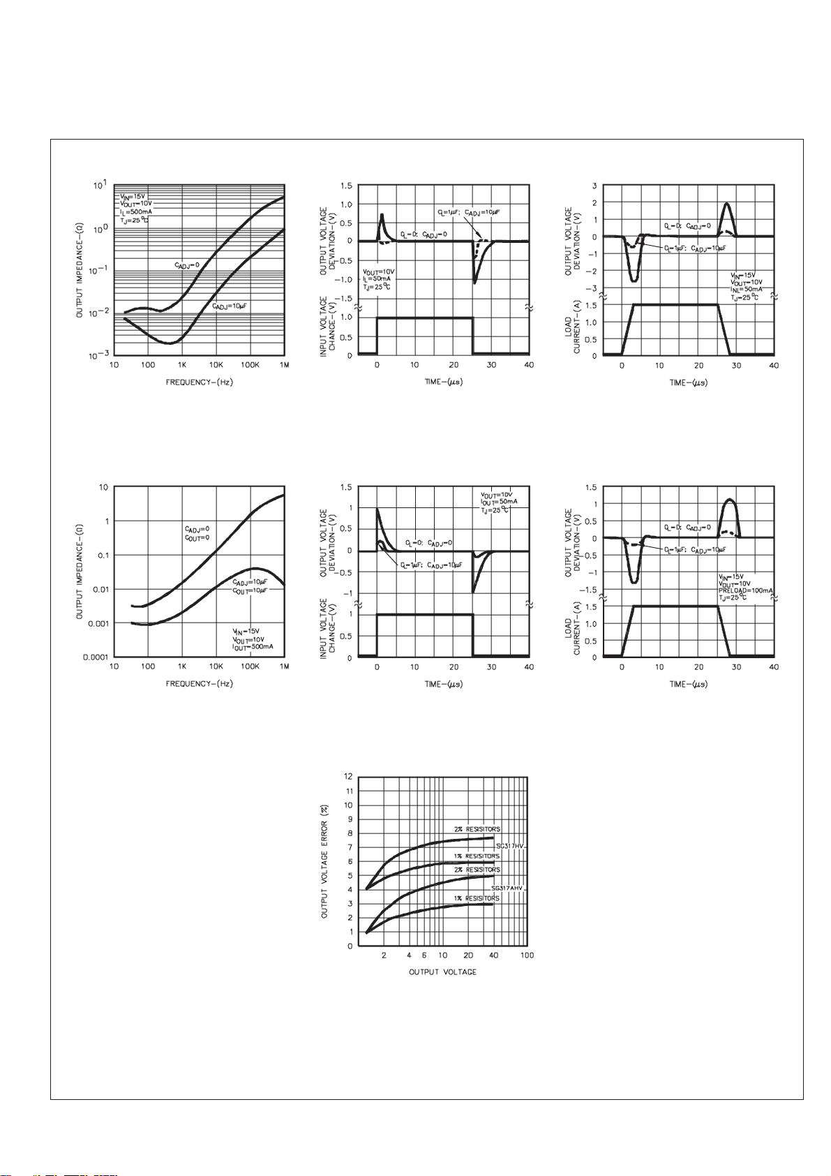
FIGURE 6.
QUISCENT CURRENT VS. INPUT/OUTPUT
DIFFERENTIAL
FIGURE 5.
REFERENCE VOLTAGE VS. TEMPERATURE
FIGURE 3.
ADJUSTMENT CURRENT VS. TEMPERATURE
FIGURE 2.
OUTPUT CURRENT VS. INPUT/OUTPUT
DIFFERENTIAL
FIGURE 1.
OUTPUT VOLTAGE DEVIATION VS. TEMPERATURE
FIGURE 4.
INPUT/OUTPUT DIFFERENTIAL VS. TEMPERATURE
FIGURE 9.
RIPPLE REJECTION VS. OUTPUT CURRENT
FIGURE 7.
RIPPLE REJECTION VS. OUTPUT VOLTAGE
FIGURE 8.
RIPPLE REJECTION VS. FREQUENCY
CHARACTERISTIC CURVES
SG117A/SG117 SERIES
2/93 Rev 1.2 10/02 LINFINITY Microelectronics Inc.
Copyright 1994 11861 Western Avenue
∞ ∞
∞ ∞
∞ Garden Grove, CA 92841
5 (714) 898-8121
∞∞
∞∞
∞ FAX: (714) 893-2570
FIGURE 15.
LOAD TRANSIENT RESPONSE
FIGURE 14.
LINE TRANSIENT RESPONSE
FIGURE 13.
OUTPUT IMPEDANCE VS. FREQUENCY
FIGURE 12.
LOAD TRANSIENT RESPONSE
FIGURE 11.
LINE TRANSIENT RESPONSE
FIGURE 10.
OUTPUT IMPEDANCE VS. FEQUENCY
CHARACTERISTIC CURVES (continued)
FIGURE 16.
OUTPUT VOLTAGE ERROR

SG117A/SG117 SERIES
2/93 Rev 1.2 10/02 LINFINITY Microelectronics Inc.
Copyright 1994 11861 Western Avenue
∞ ∞
∞ ∞
∞ Garden Grove, CA 92841
6 (714) 898-8121
∞∞
∞∞
∞ FAX: (714) 893-2570
APPLICATION INFORMATION
GENERAL
The SG117A develops a 1.25V reference voltage between the
output and the adjustable terminal (see Figure 1). By placing a
resistor, R
1
between these two terminals, a constant current is
caused to flow through R
1
and down through R2 to set the overall
output voltage, Normally this current is the specified minimum
load current of 5mA or 10mA.
FIGURE 17 - BASIC REGULATOR CIRCUIT
Because I
ADJ
is very small and constant when compared with the
current through R
1
, it represents a small error and can usually be
ignored.
It is easily seen from the above equation, that even if the resistors
were of exact value, the accuracy of the output is limited by the
accuracy of V
REF
. Earlier adjustable regulators had a reference
tolerance of ±4%. This tolerance is dangerously close to the ±5%
supply tolerance required in many logic and analog systems.
Further, many 1% resistors can drift 0.01%°C adding another 1%
to the output voltage tolerance.
For example, using 2% resistors and ±4% tolerance for VREF,
calculations will show that the expected range of a 5V regulator
design would be 4.66V ≤ V
OUT
≤ 5.36V or approximately ±7%. If
the same example were used for a 15V regulator, the expected
tolerance would be ±8%. With these results most applications
require some method of trimming, usually a trim pot. This solution
is expensive and not conducive to volume production.
One of the enhancements of Silicon General’s adjustable regulators over existing devices is tightened initial tolerance. This
allows relatively inexpensive 1% or 2% film resistors to be used
for R
1
and R2 while setting output voltage within an acceptable
tolerance range.
With a guaranteed 1% reference, a 5V power supply design,
using ±2% resistors, would have a worse case manufacturing
tolerance of ±4%. If 1% resistors were used, the tolerance would
drop to ±2.5%. A plot of the worst case output voltage tolerance
as a function of resistor tolerance is shown on the front page.
1.00 1.47 2.15 3.16 4.64 6.81
1.02 1.50 2.21 3.24 4.75 6.98
1.05 1.54 2.26 3.32 4.87 7.15
1.07 1.58 2.32 3.40 4.99 7.32
1.10 1.62 2.37 3.48 5.11 7.50
1.13 1.65 2.43 3.57 5.23 7.68
1.15 1.69 2.49 3.65 5.36 7.87
1.18 1.74 2.55 3.74 5.49 8.06
1.21 1.78 2.61 3.83 5.62 8.25
1.24 1.82 2.67 3.92 5.76 8.45
1.27 1.87 2.74 4.02 5.90 8.66
1.30 1.91 2.80 4.12 6.04 8.87
1.33 1.96 2.87 4.22 6.19 9.09
1.37 2.00 2.94 4.32 6.34 9.31
1.40 2.05 3.01 4.42 6.49 9.53
1.43 2.10 3.09 4.53 6.65 9.76
Table of ½% and 1% Standard Resistance Values
Standard Resistance Values are obtained from the Decade
Table by multiplying by multiples of 10. As an example:1.21
can represent 1.21Ω, 12.1Ω, 121Ω, 1.21KΩ etc.
FIGURE 18 - CONNECTIONS FOR BEST LOAD REGULATION
FIGURE 19 - 1.2V-25V ADJUSTABLE REGULATOR
For convenience, a table of standard 1% resistor values is shown
below.

SG117A/SG117 SERIES
2/93 Rev 1.2 10/02 LINFINITY Microelectronics Inc.
Copyright 1994 11861 Western Avenue
∞ ∞
∞ ∞
∞ Garden Grove, CA 92841
7 (714) 898-8121
∞∞
∞∞
∞ FAX: (714) 893-2570
APPLICATION INFORMATION (continued)
BYPASS CAPACITORS
Input bypassing using a 1µF tantalum or 25µF electrolytic is
recommended when the input filter capacitors are more than 5
inches from the device. A 0.1µF bypass capacitor on the
ADJUST pin is required if the load current varies by more than 1A/
µsec. Improved ripple rejection (80dB) can be accomplished by
adding a 10µF capacitor from the adjust pin to ground. For
improved AC transient response and to prevent the possibility of
oscillation due to unknown reactive load, a 1µF capacitor is also
recommended at the output. Because of their low impedance at
high frequencies, the best type of capacitor to use is solid
tantalum.
FIGURE 22 - 5V REGULATOR WITH SHUT DOWN
FIGURE 23 - 21V PROGRAMMING SUPPLY FOR UV PROM/EEPROM
FIGURE 24 - 2816 EEPROM SUPPLY PROGRAMMER FOR READ/WRITE CONTROL
FIGURE 25 - TEMPERATURE COMPENSATED LEAD ACID BATTERY CHARGER
FIGURE 21 - IMPROVING RIPPLE REJECTION
LOAD REGULATION
Because the SG117A is a three-terminal device, it is not possible
to provide true remote load sensing. Load regulation will be
limited by the resistance of the wire connecting the regulator to
the load. For the data sheet specification, regulation is measured
at the bottom of the package. Negative side sensing is a true
Kelvin connection, with the bottom of the output divider returned
to the negative side of the load. Although it may not be immediately obvious, best load regulation is obtained when the top of the
divider is connected directly to the case, not to the load. This is
illustrated in Figure 18. If R
1
were connected to the load, the
effective resistance between the regulator and the load would be
Connected as shown, RP is not multiplied by the divider ratio. R
P
is about 0.004Ω per foot using 16 gauge wire. This translates to
4mV/ft. at 1A load current, so it is important to keep the positive
lead between regulator and load as short as possible.
FIGURE 20 - REMOTE SENSING
( )
RP X ,RP = Parasitic Line Resistance.
R2 + R
1
R
1

SG117A/SG117 SERIES
2/93 Rev 1.2 10/02 LINFINITY Microelectronics Inc.
Copyright 1994 11861 Western Avenue
∞ ∞
∞ ∞
∞ Garden Grove, CA 92841
8 (714) 898-8121
∞∞
∞∞
∞ FAX: (714) 893-2570
CONNECTION DIAGRAMS & ORDERING INFORMATION (See Notes Below)
Ambient
Temperature Range
Part No.Package
Connection Diagram
3-TERMINAL TO-3
METAL CAN
K-PACKAGE
SG117AK/883B -55°C to 125°C
SG117AK/DESC -55°C to 125°C
SG117AK -55°C to 125°C
SG217AK -25°C to 85°C
SG317AK 0°C to 70°C
SG117K/883B -55°C to 125°C
JAN117K -55°C to 125°C
SG117K/DESC -55°C to 125°C
SG117K -55°C to 125°C
SG217K -25°C to 85°C
SG317K 0°C to 70°C
2
1
ADJUSTMENT
CASE IS V
OUT
V
IN
3-TERMINAL TO-66
METAL CAN
R-PACKAGE
SG117AR/883B -55°C to 125°C
SG117AR/DESC -55°C to 125°C
SG117AR -55°C to 125°C
SG217AR -25°C to 85°C
SG317AR 0°C to 70°C
SG117R/883B -55°C to 125°C
SG117AR/DESC -55°C to 125°C
SG117R -55°C to 125°C
SG217R -25°C to 85°C
SG317R 0°C to 70°C
1
2
ADJUSTMENT
CASE IS V
OUT
V
IN
3-PIN TO-39 METAL CAN
T-PACKAGE
SG117AT/883B -55°C to 125°C
SG117AT/DESC -55°C to 125°C
SG117AT -55°C to 125°C
SG217AT -25°C to 85°C
SG317AT 0°C to 70°C
SG117T/883B -55°C to 125°C
JAN117T -55°C to 125°C
SG117T/DESC -55°C to 125°C
SG117T -55°C to 125°C
SG217T -25°C to 85°C
SG317T 0°C to 70°C
V
OUT
ADJUST
32
1V
IN
CASE IS V
OUT
3-PIN HERMETIC TO-257
IG-PACKAGE (Isolated)
SG117AIG/883B -55°C to 125°C
SG117AIG/DESC -55°C to 125°C
SG117AIG -55°C to 125°C
SG117IG/883B -55°C to 125°C
SG117IG/DESC -55°C to 125°C
SG117IG -55°C to 125°C
V
IN
V
OUT
ADJUST
SG117AL/883B -55°C to 125°C
SG117AL/DESC -55°C to 125°C
SG117AL -55°C to 125°C
SG117L/883B -55°C to 125°C
SG117L/DESC -55°C to 125°C
SG117L -55°C to 125°C
20-PIN CERAMIC (LCC)
LEADLESS CHIP CARRIER
L- PACKAGE
4
5
6
7
8
18
17
16
15
14
9 10111213
32 12019 11. N.C.
12. N.C.
13. N.C.
14. N.C.
15. N.C.
16. N.C.
17. N.C.
18. N.C.
19. N.C.
20. V
OUT
(Note 4) 1. V
OUT
SENSE
2. N.C.
3. N.C.
4. N.C.
5. V
IN
6. N.C.
7. N.C.
8. N.C.
9. N.C.
10. ADJUST
Note 1. Contact factory for JAN and DESC product availability.
2. All parts are viewed from the top.
3. Both inputs and outputs must be externally connected together at the device
terminals.
4. For normal operation the SENSE pin must be externally connected to the load.
 Loading...