

Page 1
查询SG1842供应商
LIN DOC #: 1842
SG1842/SG1843 Series
C
URRENT MODE
PWM C
ONTROLLER
T HE I NFINITE P OWER OF I NNOVATION
DESCRIPTION KEY FEATURES
The SG1842/43 family of control IC's
provides all the necessary features to
implement off-line fixed frequency,
current-mode switching power supplies
with a minimum number of external
components. Current-mode
architecture demonstrates improved
line regulation, improved load
regulation, pulse-by-pulse current
limiting and inherent protection of the
power supply output switch.
The bandgap reference is trimmed to
±1% over temperature. Oscillator
discharge current is trimmed to less
than ±10%. The SG1842/43 has under-
voltage lockout, current limiting
circuitry and start-up current of less
than 1mA.
The totem-pole output is optimized
to drive the gate of a power MOSFET.
The output is low in the off state to
provide direct interface to an N
channel device.
The SG1842/43 is specified for
operation over the full military ambient
temperature range of -55°C to 125°C.
The SG2842/43 is specified for the
industrial range of -25°C to 85°C, and
the SG3842/43 is designed for the
commercial range of 0°C to 70°C.
PRODUCT HIGHLIGHT
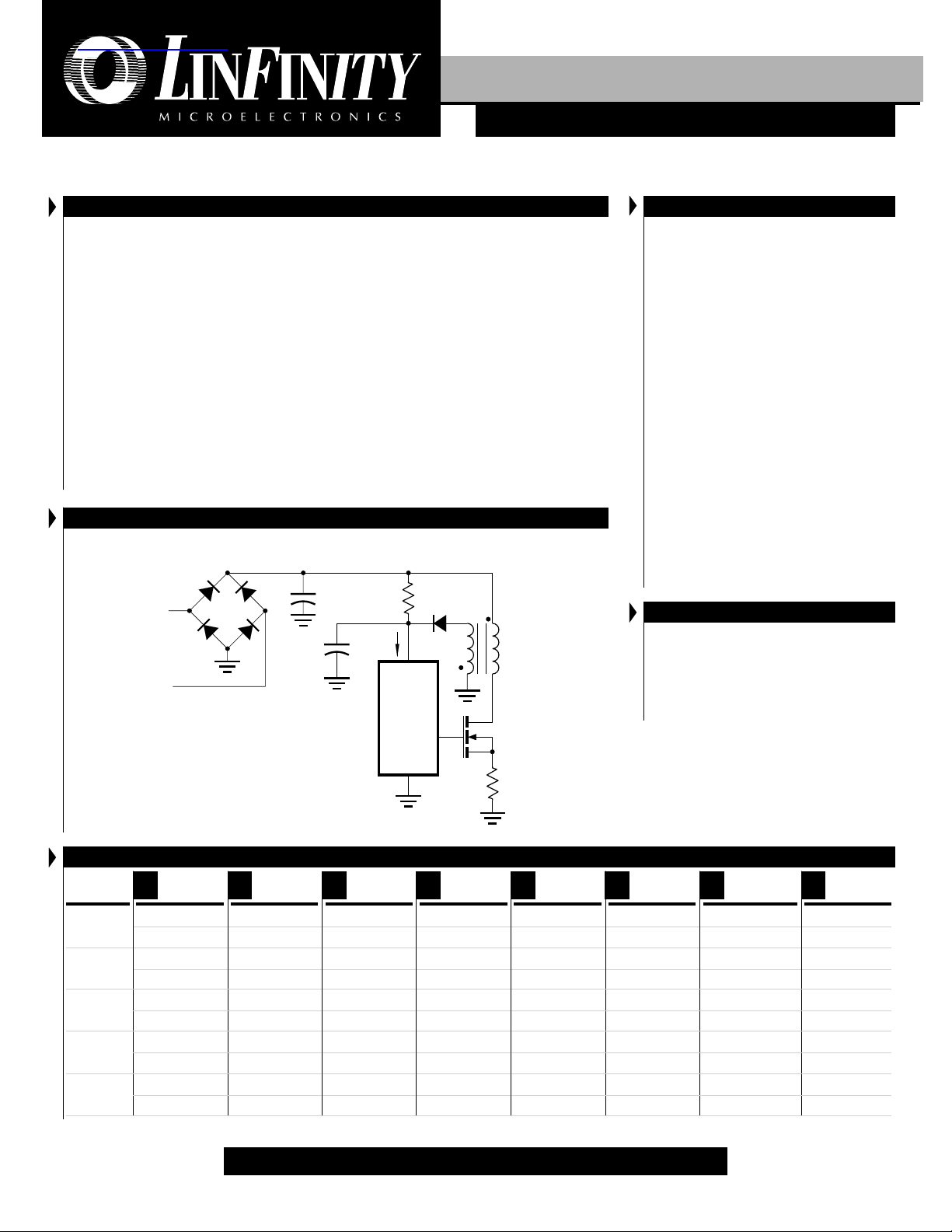
TYPICAL APPLICATION OF SG3842 IN A FLYBACK CONVERTER
R
AC
INPUT
I
V
CC
SG3842
ST
P RODUCTION DATA SHEET
■ OPTIMIZED FOR OFF-LINE CONTROL
■ LOW START-UP CURRENT (<1mA)
■ AUTOMATIC FEED FORWARD
COMPENSATION
■ TRIMMED OSCILLATOR DISCHARGE
CURRENT
■ PULSE-BY-PULSE CURRENT LIMITING
■ ENHANCED LOAD RESPONSE
CHARACTERISTICS
■ UNDER-VOLTAGE LOCKOUT WITH 6V
HYSTERESIS (SG1842 only)
■ DOUBLE-PULSE SUPPRESSION
■ HIGH-CURRENT TOTEM-POLE OUTPUT
(1AMP PEAK)
■ INTERNALLY TRIMMED BANDGAP
REFERENCE
■ 500KHZ OPERATION
■ UNDERVOLTAGE LOCKOUT
SG1842 - 16 volts
SG1843 - 8.4 volts
■ LOW SHOOT-THROUGH CURRENT <75mA
OVER TEMPERATURE
ST
HIGH RELIABILITY FEATURES
■ AVAILABLE TO MIL-STD-883B AND DESC
SMD
■ SCHEDULED FOR MIL-M38510 QPL LISTING
■ RADIATION DATA AVAILABLE
■
LINFINITY LEVEL "S" PROCESSING AVAILABLE
(°C)
T
A
0 to 70
-25 to 85
-55 to 125
MIL-STD/883
DESC
Copyright © 2000
Rev. 1.6 4/00
PACKAGE ORDER INFORMATION
Plastic DIP
M
8-pin
SG3842M SG3842N SG3842DM SG3842D SG3842Y SG3842J — —
SG3843M SG3843N SG3843DM SG3843D SG3843Y SG3843J — —
SG2842M SG2842N SG2842DM SG2842D SG2842Y SG2842J — —
SG2843M SG2843N SG2843DM SG2843D SG2843Y SG2843J — —
— — — — SG1842Y SG1842J — SG1842L
— — — — SG1843Y SG1843J — SG1843L
— — — — SG1842Y/883B SG1842J/883B — SG1842L/883B
— — — — SG1843Y/883B SG1843J/883B — SG1843L/883B
— — — — SG1842Y/DESC SG1842J/DESC SG1842F/DESC SG1842L/DESC
Plastic DIP
N
14-pin
Plastic SOIC
DM
8-pin
— — SG1843Y/DESC SG1843J/DESC SG1843F/DESC SG1843L/DESC
Note: All surface-mount packages are available in Tape & Reel.
Plastic SOIC
D
14-pin
Ceramic DIP
Y
8-pin
Ceramic DIP
J
14-pin
Cer. Flatpack
F
10-pin
L
FOR FURTHER INFORMATION CALL (714) 898-8121
11861 WESTERN AVENUE, GARDEN GROVE, CA. 92841
Ceramic LCC
20-pin
1
Page 2
PRODUCT DATABOOK 1996/1997
SG1842/SG1843 Series
C
URRENT-MODE
P RODUCTION DATA SHEET
PWM C
ONTROLLER
ABSOLUTE MAXIMUM RATINGS (Notes 1 & 2)
Supply Voltage (ICC < 30mA) ...............................................................Self Limiting
Supply Voltage (Low Impedance Source) ........................................................ 30V
Output Current (Peak) .......................................................................................±1A
Output Current (Continuous) .......................................................................350mA
Output Energy (Capacitive Load) ....................................................................... 5µJ
Analog Inputs (Pins 2, 3) ................................................................. -0.3V to +6.3V
Error Amp Output Sink Current .....................................................................10mA
Power Dissipation at TA = 25°C (DIL-8) ............................................................ 1W
Operating Junction Temperature
Hermetic (J, Y, F, L Packages) ................................................................... 150°C
Plastic (N, M, D, DM Packages) ................................................................ 150°C
Storage Temperature Range .......................................................... -65°C to +150°C
Lead Temperature (Soldering, 10 Seconds) .................................................. 300°C
Note 1. Exceeding these ratings could cause damage to the device.
Note 2. All voltages are with respect to Pin 5. All currents are positive into the specified
terminal.
THERMAL DATA
M PACKAGE:
THERMAL RESISTANCE-JUNCTION TO AMBIENT,
N PACKAGE:
THERMAL RESISTANCE-JUNCTION TO AMBIENT,
DM PACKAGE:
THERMAL RESISTANCE-JUNCTION TO AMBIENT,
D PACKAGE:
THERMAL RESISTANCE-JUNCTION TO AMBIENT,
Y PACKAGE:
THERMAL RESISTANCE-JUNCTION TO AMBIENT,
J PACKAGE:
THERMAL RESISTANCE-JUNCTION TO AMBIENT,
F PACKAGE:
THERMAL RESISTANCE-JUNCTION TO CASE,
THERMAL RESISTANCE-JUNCTION TO AMBIENT,
L PACKAGE:
THERMAL RESISTANCE-JUNCTION TO CASE,
THERMAL RESISTANCE-JUNCTION TO AMBIENT,
Junction Temperature Calculation: TJ = TA + (PD x θJA).
The θJA numbers are guidelines for the thermal performance of the device/pc-board
system. All of the above assume no ambient airflow.
θθ
θ
θθ
JA
θθ
θ
θθ
JA
θθ
θ
θθ
JA
θθ
θ
θθ
JA
θθ
θ
θθ
JA
θθ
θ
θθ
JA
θθ
θ
θθ
JC
θθ
θ
θθ
JA
θθ
θ
θθ
JC
θθ
θ
θθ
JA
95°C/W
65°C/W
165°C/W
120°C/W
130°C/W
80°C/W
80°C/W
145°C/W
35°C/W
120°C/W
1. COMP
2. V
FB
3. I
SENSE
4. RT/C
T
5. POWER GND
32
4
5
6
7
8
91110
PACKAGE PIN OUTS
1 8
COMP
27
V
FB
36
I
SENSE
45
RT/C
T
M & Y PACKAGE
(Top View)
SENSE
V
FB
T
1 8
27
36
45
COMP
I
RT/C
DM PACKAGE
(Top View)
N.C.
V
N.C.
I
SENSE
N.C.
FB
T
1 14
213
312
411
510
69
78
COMP
RT/C
D PACKAGE
(Top View)
1 14
COMP
213
N.C.
312
V
FB
411
N.C.
510
I
SENSE
69
N.C.
78
RT/C
T
J & N PACKAGE
(Top View)
1 10
29
38
47
56
F PACKAGE
(Top View)
12019
12 13
L PACKAGE
(Top View)
V
REF
V
CC
OUTPUT
GND
V
REF
V
CC
OUTPUT
GND
V
REF
N.C.
V
CC
V
C
OUTPUT
GND
PWR GND
V
REF
N.C.
V
CC
V
C
OUTPUT
GROUND
POWER GND
1. N.C.
2. COMP
3. N.C.
18
4. N.C.
17
5. V
16
15
14
FB
6. N.C.
7. I
SENSE
8. N.C.
9. N.C.
10. RT/C
T
10.V
REF
9. V
CC
8. V
C
7. OUTPUT
6. GND
11. N.C.
12. GROUND
13. N.C.
14. N.C.
15. OUTPUT
16. N.C.
17. V
CC
18. N.C.
19. N.C.
20. V
REF
2
Copyright © 2000
Rev. 1.6 4/00
Page 3
PRODUCT DATABOOK 1996/1997
SG1842/SG1843 Series
C
URRENT-MODE
P RODUCTION DATA SHEET
RECOMMENDED OPERATING CONDITIONS (Note 3)
PWM C
ONTROLLER
Parameter
Symbol
Supply Voltage Range
Output Current (Peak)
Output Current (Continuous)
Analog Inputs (Pin 2, Pin 3)
Error Amp Output Sink Current
Oscillator Frequency Range
Oscillator Timing Resistor R
Oscillator Timing Capacitor C
T
T
Recommended Operating Conditions
Min. Typ. Max.
Units
30 V
±1 A
200 mA
02.6V
5mA
0.1 500 kHz
0.52 150 KΩ
0.001 1.0 µF
Operating Ambient Temperature Range:
SG1842/43
SG2842/43
SG3842/43
-55 125 °C
-25 85 °C
070°C
Note 3. Range over which the device is functional.
ELECTRICAL CHARACTERISTICS
(Unless otherwise specified, these specifications apply over the operating ambient temperatures for SG1842/SG1843 with -55°C ≤ TA ≤ 125°C, SG2842/
SG2843 with -25°C ≤ TA ≤ 85°C, SG3842/SG3843 with 0°C ≤ TA ≤ 70°C, VCC = 15V (Note 7), RT = 10kΩ, and CT = 3.3nF. Low duty cycle pulse testing
techniques are used which maintains junction and case temperatures equal to the ambient temperature.)
Parameter
Symbol
Test Conditions
SG1842/43
SG2842/43
Min. Typ. Max. Min. Typ. Max. Min. Typ. Max.
SG3842/43
Units
Reference Section
Output Voltage TJ = 25°C, IO = 1mA
Line Regulation 12 ≤ VIN ≤ 25V
Load Regulation 1 ≤ IO ≤ 20mA
Temperature Stability (Note 4)
Total Output Variation (Note 4) Line, Load, Temp.
Output Noise Voltage (Note 4) VN10Hz ≤ f ≤ 10kHz, TJ = 25°C
Long Term Stability (Note 4) TA = 125°C, 1000hrs
Output Short Circuit
4.95 5.00 5.05 4.95 5.00 5.05 4.90 5.00 5.10 V
620 620 620 mV
625 625 625 mV
0.2 0.4 0.2 0.4 0.2 0.4 mV/°C
4.90 5.10 4.90 5.10 4.82 5.18 V
50 50 50 µV
525 525 525 mV
-30 -100 -180 -30 -100 -180 -30 -100 -180 mA
Oscillator Section
Initial Accuracy TJ = 25°C
Voltage Stability 12 ≤ VCC ≤ 25V
Temperature Stability (Note 4) T
Amplitude V
≤ TA ≤ T
MIN
(Peak to Peak)
RT/CT
MAX
Discharge Current TJ = 25°C
T
≤ TA ≤ T
MIN
MAX
47 52 57 47 52 57 47 52 57 kHz
0.2 1 0.2 1 0.2 1 %
555%
1.7 1.7 1.7 V
7.8 8.3 8.8 7.5 8.4 9.3 7.5 8.4 9.3 mA
7.0 9.0 7.2 9.5 7.2 9.5 mA
Error Amp Section
Input Voltage V
Input Bias Current
Open Loop Gain A
VOL
Unity Gain Bandwidth (Note 4) TJ = 25°C
Power Supply Rejection Ratio PSRR 12 ≤ VCC ≤ 25V
Output Sink Current V
Output Source Current V
V
High V
OUT
V
Low V
OUT
= 2.5V
COMP
2 ≤ VO ≤ 4V
= 2.7V, V
VFB
= 2.3V, V
VFB
= 2.3V, RL = 15K to gnd
VFB
= 2.7V, RL = 15K to V
VFB
COMP
COMP
= 1.1V
= 5V
2.45 2.50 2.55 2.45 2.50 2.55 2.42 2.50 2.58 V
-0.3 -1 -0.3 1 -0.3 -2 µA
65 90 65 90 65 90 dB
0.7 1 0.7 1 0.7 1 MHz
60 70 60 70 60 70 dB
26 26 26 mA
-0.5 -0.8 -0.5 -0.8 -0.5 -0.8 mA
56 56 56 V
REF
0.7 1.1 0.7 1.1 0.7 1.1 V
(Electrical Characteristics continue next page.)
Copyright © 2000
Rev. 1.6 4/00
3
Page 4
PRODUCT DATABOOK 1996/1997
SG1842/SG1843 Series
C
URRENT-MODE
P RODUCTION DATA SHEET
ELECTRICAL CHARACTERISTICS (Cont'd.)
PWM C
ONTROLLER
Parameter
Symbol
Test Conditions
Current Sense Section
Gain (Notes 5 & 6)
Maximum Input Signal (Note 5) V
Power Supply Rejection Ratio (Note 5) PSRR 12 ≤ V
Input Bias Current
Delay to Output (Note 4)
COMP
= 5V
CC
≤ 25V
Output Section
Output Low Level I
Output High Level I
Rise Time TJ = 25°C, CL = 1nF
Fall Time TJ = 25°C, CL = 1nF
= 20mA
SINK
I
= 200mA
SINK
SOURCE
I
SOURCE
= 20mA
= 200mA
Under-Voltage Lockout Section
Start Threshold 1842
1843
Min. Operation Voltage After Turn-On 1842
1843
PWM Section
Maximum Duty Cycle
Minimum Duty Cycle
Power Consumption Section
Start-Up Current
Operating Supply Current VFB = V
VCC Zener Voltage ICC = 25mA
Notes: 4. These parameters, although guaranteed, are not 100% tested in
production.
5. Parameter measured at trip point of latch with V
ISENSE
VFB
= 0V
= 0.
SG1842/43
SG2842/43
Min. Typ. Max. Min. Typ. Max. Min. Typ. Max.
2.85 3 3.15 2.85 3 3.15 2.85 3 3.15 V/V
0.9 1 1.1 0.9 1 1.1 0.9 1 1.1 V
70 70 70 dB
-2 -10 -2 -10 -2 -10 µA
150 300 150 300 150 300 ns
0.1 0.4 0.1 0.4 0.1 0.4 V
1.5 2.2 1.5 2.2 1.5 2.2 V
13 13.5 13 13.5 13 13.5 V
12 13.5 12 13.5 12 13.5 V
50 150 50 150 50 150 ns
50 150 50 150 50 150 ns
15 16 17 15 16 17 14.5 16 17.5 V
7.8 8.4 9.0 7.8 8.4 9.0 7.8 8.4 9.0 V
9 10 11 9 10 11 8.5 10 11.5 V
7.0 7.6 8.3 7.0 7.6 8.2 7.0 7.6 8.2 V
93 95 100 90 95 100 90 95 100 %
000%
0.5 1 0.5 1 0.5 1 mA
11 17 11 17 11 17 mA
34 34 34 V
∆ V
6. Gain defined as: A = ; 0 ≤ V
7. Adjust VCC above the start threshold before setting at 15V.
∆ V
COMP
ISENSE
SG3842/43
≤ 0.8V.
ISENSE
Units
4
Copyright © 2000
Rev. 1.6 4/00
Page 5
V
CC
GROUND**
PRODUCT DATABOOK 1996/1997
SG1842/SG1843 Series
C
URRENT-MODE
P RODUCTION DATA SHEET
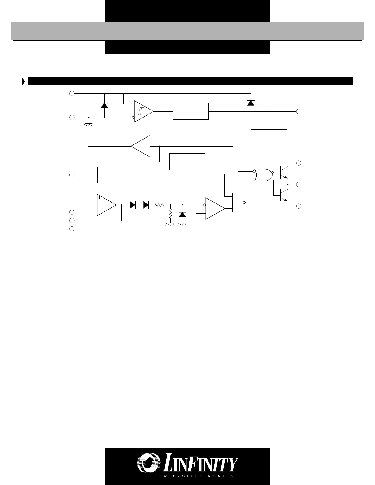
BLOCK DIAGRAM
*
34V
16V (1842)
8.4V (1843)
2.5V
UVLO
6V (1842)
0.8V (1843)
PWM C
S / R
V
REF
GOOD LOGIC
ONTROLLER
5V
REF
INTERNAL
BIAS
V
REF
5.0V
50mA
V
*
C
R
T/CT
V
FB
COMP
CURRENT SENSE
- V
and VC are internally connected for 8 pin packages.
*
CC
- POWER GROUND and GROUND are internally connected for 8 pin packages.
**
OSCILLATOR
ERROR AMP
2R
R
1V
S
R
CURRENT SENSE
COMPARATOR
PWM
LATCH
OUTPUT
POWER GROUND**
Copyright © 2000
Rev. 1.6 4/00
5
Page 6

PRODUCT DATABOOK 1996/1997
SG1842/SG1843 Series
C
URRENT-MODE
P RODUCTION DATA SHEET
PWM C
ONTROLLER
GRAPH / CURVE INDEX
Characteristic Curves
FIGURE #
1. DROPOUT VOLTAGE vs. TEMPERATURE
2. OSCILLATOR TEMPERATURE STABILITY
3. CURRENT SENSE TO OUTPUT DELAY vs. TEMPERATURE
4. OUTPUT DUTY CYCLE vs. TEMPERATURE
5. START-UP CURRENT vs. TEMPERATURE
6. REFERENCE VOLTAGE vs. TEMPERATURE
7. START-UP VOLTAGE THRESHOLD vs. TEMPERATURE
8. START-UP VOLTAGE THRESHOLD vs. TEMPERATURE
9. OSCILLATOR DISCHARGE CURRENT vs. TEMPERATURE
10. OUTPUT SATURATION VOLTAGE vs. OUTPUT CURRENT AND
TEMPERATURE (SINK TRANSISTOR)
11. CURRENT SENSE THRESHOLD vs. ERROR AMPLIFIER OUTPUT
12. OUTPUT SATURATION VOLTAGE vs. OUTPUT CURRENT AND
TEMPERATURE (SOURCE TRANSISTOR)
FIGURE INDEX
Application Information
FIGURE #
13. OSCILLATOR TIMING CIRCUIT
14. OSCILLATOR FREQUENCY vs. R
FOR VARIOUS C
T
T
Typical Applications Section
FIGURE #
15. CURRENT SENSE SPIKE SUPPRESSION
16. MOSFET PARASITIC OSCILLATIONS
17. BIPOLAR TRANSISTOR DRIVE
18. ISOLATED MOSFET DRIVE
19. ADJUSTABLE BUFFERED REDUCTION OF CLAMP LEVEL WITH
SOFTSTART
20. EXTERNAL DUTY CYCLE CLAMP AND MULTI-UNIT
SYNCHRONIZATION
21. OSCILLATOR CONNECTION
22. ERROR AMPLIFIER CONNECTION
23. SLOPE COMPENSATION
24. OPEN LOOP LABORATORY FIXTURE
25. OFF-LINE FLYBACK REGULATOR
6
Copyright © 2000
Rev. 1.6 4/00
Page 7

PRODUCT DATABOOK 1996/1997
SG1842/SG1843 Series
C
URRENT-MODE
P RODUCTION DATA SHEET
CHARACTERISTIC CURVES
PWM C
ONTROLLER
FIGURE 1. — DROPOUT VOLTAGE vs. TEMPERATURE
10.0
SG1842
9.6
9.2
8.8
8.4
Minimum Operating Voltage - (V)
8.0
-50-25 0255075100125
-75
SG1843
Junction Temperature - (°C)
FIGURE 3. — CURRENT SENSE TO OUTPUT DELAY vs.
TEMPERATURE
FIGURE 2. — OSCILLATOR TEMPERATURE STABILITY
2
0
-2
-4
-6
-8
Frequency Drift - (%)
-10
-50-25 0255075100125
-75
VIN = 15V
Duty Cycle = 50%
Junction Temperature - (°C)
FIGURE 4. — OUTPUT DUTY CYCLE vs. TEMPERATURE
Current Sense Delay - (nS)
Copyright © 2000
Rev. 1.6 4/00
220
200
180
160
140
120
V
PIN3
-50-25 0255075100125
-75
Junction Temperature - (°C)
= 1.1V
200kHz
50
49
48
47
46
45
Output Duty Cycle - (%)
44
-50-25 0255075100125
-75
100kHz
50kHz
Junction Temperature - (°C)
50kHz
100kHz
200kHz
7
Page 8

PRODUCT DATABOOK 1996/1997
Junction Temperature - (°C)
Start Up Voltage - (V)
16.00
-75
-50-25 0255075100125
SG1842
16.02
16.04
16.06
16.08
15.98
SG1842/SG1843 Series
C
URRENT-MODE
P RODUCTION DATA SHEET
CHARACTERISTIC CURVES
PWM C
ONTROLLER
FIGURE 5. — START-UP CURRENT vs. TEMPERATURE
0.7
SG1842
0.6
0.5
0.4
0.3
Start-Up Current - (mA)
0.2
-50-25 0255075100125
-75
SG1843
Junction Temperature - (°C)
FIGURE 7. — START-UP VOLTAGE THRESHOLD vs.
TEMPERATURE
FIGURE 6. — REFERENCE VOLTAGE vs. TEMPERATURE
5.02
5.01
VCC = 15V
5.00
4.99
Reference Voltage - (V)
4.98
-75
-50-25 0255075100125
Junction Temperature - (°C)
FIGURE 8. — START-UP VOLTAGE THRESHOLD vs.
TEMPERATURE
8.32
8.30
8.28
8.26
8.24
Reference Voltage - (V)
8.22
8.20
8.18
8
SG1843
-75
-50-25 0255075100125
Junction Temperature - (°C)
Copyright © 2000
Rev. 1.6 4/00
Page 9

PRODUCT DATABOOK 1996/1997
SG1842/SG1843 Series
C
URRENT-MODE
P RODUCTION DATA SHEET
CHARACTERISTIC CURVES
PWM C
ONTROLLER
FIGURE 9. — OSCILLATOR DISCHARGE CURRENT vs.
TEMPERATURE
8.2
8.0
7.8
7.6
7.4
Oscillator Discharge Current - (mA)
7.2
-75
-50-25 0255075100125
Junction Temperature - (°C)
FIGURE 11. — CURRENT SENSE THRESHOLD vs.
ERROR AMPLIFIER OUTPUT
1.0
FIGURE 10. — OUTPUT SATURATION VOLTAGE vs.
OUTPUT CURRENT & TEMPERATURE
2.5
2.0
1.5
1.0
Saturation Voltage - (V)
0.5
0
100 200 300 400 500
-55°C
+25°C
+125°C
VIN = 15V
Duty Cycle < 5%
Output Current - (mA)
FIGURE 12. — OUTPUT SATURATION VOLTAGE vs.
OUTPUT CURRENT & TEMPERATURE
Current Sense Threshold - (V)
Copyright © 2000
Rev. 1.6 4/00
0.9
0.8
0.7
0.6
0.5
0.4
0.3
0.2
0.1
4.0
125°C
25°C
-55°C
3.0
2.0
Saturation Voltage - (V)
1.0
0
1.0 2.0 3.0 4.0 5.0
0
Error Amp Output Voltage - (V)
VIN = 15V
Duty Cycle < 5%
+125°C
+25°C
-55°C
+25°C
+125°C
100 200 300 400 500
Output Current - (mA)
9
Page 10

PRODUCT DATABOOK 1996/1997
T
SG1842/SG1843 Series
C
URRENT-MODE
P RODUCTION DATA SHEET
APPLICATION INFORMATION
OSCILLATOR
The oscillator of the 1842/43 family of PWM's is designed such
that many values of R
frequency, but only one combination will yield a specific duty
cycle at a given frequency.
Given: Frequency ≡ f
Maximum Duty Cycle ≡ D
Calculate: RT = 267 (Ω)
CT = (µF)
For Duty-Cycles above 95% use:
and CT will give the same oscillator
T
m
1/D
(1-Dm)/D
m
-1
m
- 1
(1.76)
(1.76)
where .3 < Dm < .95
1.86 * D
f * R
V
RT/C
T
REF
m
RT
T
C
GND
PWM C
CT for a given frequency and maximum duty cycle. (Note: These
formulas are less accurate for smaller duty cycles or higher
frequencies. This will require trimming of RT or CT to correct for
this error.)
Example:
cycle at a switching frequency of 50kHz. What are the values
of RT and CT?
Given: f = 50kHz
Calculate: RT = 267 = 674Ω
1000
100
f - (kHz)
10
ONTROLLER
A set of formulas are given to determine the values of RT and
A Flyback power supply requires a maximum of 45% duty
Dm = 0.45
1/.045
(1.76)
.55/.45
(1.76)
1.86 * 0.45
CT = = .025µF
50000 * 674
R
= 680
T
R
= 2k
T
R
= 5k
T
R
= 10k
T
R
= 20k
T
R
= 30k
T
R
= 50k
T
R
= 70k
T
R
= 100k
T
-1
- 1
10
1.86
F ≈ where RT ≥ 5kΩ
R
TCT
FIGURE 13 — OSCILLATOR TIMING CIRCUIT
1
.001
.002 .02
.005 .01 .05 0.1
CT Value - (µF)
FIGURE 14 — OSCILLATOR FREQUENCY vs. RT FOR VARIOUS C
T
Copyright © 2000
Rev. 1.6 4/00
Page 11

PRODUCT DATABOOK 1996/1997
VINV
CC
7 (12)
7 (11)
6 (10)
5 (8)
R
S
Q1
SG1842/43
3 (5)
R
1
V
CC
V
IN
7 (12)
7 (11)
6 (10)
5 (8)
3 (5)
SG1842/43
Isolation
Boundary
C
R
R
S
N
S
N
P
Q1
Waveforms
+
_
0
+
_
0
50% DC
25% DC
SG1842/SG1843 Series
C
URRENT-MODE
P RODUCTION DATA SHEET
TYPICAL APPLICATION CIRCUITS
Pin numbers referenced are for 8-pin package and pin numbers in parenthesis are for 14-pin package.
VCCV
IN
7 (12)
PWM C
ONTROLLER
SG1842/43
7 (11)
6 (10)
5 (8)
3 (5)
Q1
I
PK
R
1.0V
I
=
PK(MAX)
R
R
C
S
S
FIGURE 15. — CURRENT-SENSE SPIKE SUPPRESSION
The RC low pass filter will eliminate the leading edge current spike
caused by parasitics of Power MOSFET.
I
B
V
C
+
R
2
V
C1
_
R1|| R
2
SG1842/43
V
C
7 (11)
6 (10)
V
C
R
2
R
V
IN
C1
1
Q1
1
FIGURE 16. — MOSFET PARASITIC OSCILLATIONS
A resistor (R1) in series with the MOSFET gate reduce overshoot and
ringing caused by the MOSFET input capacitance and any inductance in series with the gate drive. (Note: It is very important to
have a low inductance ground path to insure correct operation of
the I.C. This can be done by making the ground paths as short and
as wide as possible.)
5 (8)
The 1842/43 output stage can provide negative base current to
remove base charge of power transistor (Q1) for faster turn off. This
is accomplished by adding a capacitor (C1) in parallel with a resistor
(R1). The resistor (R1) is to limit the base current during turn on.
Copyright © 2000
Rev. 1.6 4/00
3 (5)
R
S
V (PIN 1) - 1.4
IPK =
3R
S
N
P
N
S
FIGURE 18. — ISOLATED MOSFET DRIVEFIGURE 17. — BIPOLAR TRANSISTOR DRIVE
Current transformers can be used where isolation is required
between PWM and Primary ground. A drive transformer is then
necessary to interface the PWM output with the MOSFET.
11
Page 12

PRODUCT DATABOOK 1996/1997
A
SG1842/SG1843 Series
C
URRENT-MODE
P RODUCTION DATA SHEET
TYPICAL APPLICATION CIRCUITS (continued)
PWM C
ONTROLLER
V
7 (12)
8 (14)
4 (7)
2 (3)
1 (1)
R
2
1N4148
C
IPK = Where: VCS = 1.67 and V
t
SOFTSTART
where; V
minimum line and maximum load conditions.
MPSA63
R
1
V
CS
R
S
= -ln 1 - C
≡ voltage at the Error Amp Output under
EAO
V
EAO
5
SG1842/43
5 (9)
R
R1+R
- 1.3
R1+R
R
1
2
1
2
R1 R
R1+R
7 (11)
6 (10)
5 (8)
3 (5)
C.S.MAX
2
2
CC
= 1V (Typ.)
V
IN
Q1
I
V
CS
R
S
FIGURE 19. — ADJUSTABLE BUFFERED REDUCTION OF CLAMP LEVEL
WITH SOFTSTART
Softstart and adjustable peak current can be done with the external
circuitry shown above.
8 (14)
R
A
84
6
SG1842/43
R
B
2
f =
(RA + 2RB)C
f =
RA + 2R
1.44
R
B
555
TIMER
1
B
4 (7)
3
To other
SGX842/43
5 (9)
FIGURE 20. — EXTERNAL DUTY CYCLE CLAMP AND
MULTI-UNIT SYNCHRONIZATION
Precision duty cycle limiting as well as synchronizing several 1842/
1843's is possible with the above circuitry.
5V
2.8V
1.1V
8 (14)
R
T
4 (7)
C
SG1842/43
Discharge
Current
I
= 8.2mA
d
The oscillator is programmed by the values selected for the timing
components RT and CT. Refer to application information for
calculation of the component values.
12
2.5V
SG1842/43
0.5m
R
10K
F
2 (3)
1 (1)
R
F
T
R
i
FIGURE 22. — ERROR AMPLIFIER CONNECTIONFIGURE 21. — OSCILLATOR CONNECTION
Error amplifier is capable of sourcing and sinking current up to 0.5mA.
Copyright © 2000
Rev. 1.6 4/00
Page 13

PRODUCT DATABOOK 1996/1997
A
D
SG1842/SG1843 Series
C
URRENT-MODE
P RODUCTION DATA SHEET
TYPICAL APPLICATION CIRCUITS (continued)
PWM C
ONTROLLER
V
CC
V
IN
From V
2N222A
O
R
i
R
d
SG1842/43
5V
8(14)
R
T
R
SLOPE
C
4(7)
C
T
2(3)
R
F
F
1(1)
OSCILLATOR
ERROR
AMP
2.5V
UVLO
2R
R5VREF
R
5(9)
S
V
REF
GOOD LOGIC
1V
C.S.
COMP
PWM
LATCH
5V
INTERNAL
BIAS
7(12)
7(11)
6(10)
5(8)
3(5)
Q1
R
CR
S
FIGURE 23. — SLOPE COMPENSATION
Due to inherent instability of current mode converters running above 50% duty cycle, a slope compensation should be added to
either current sense pin or the error amplifier. Figure 23 shows a typical slope compensation technique.
V
O
V
REF
R
4.7K
ERROR AMP
DJUST
4.7K
T
COMP
1
V
2
I
3
RTC
4
SG1842/43
FB
SENSE
T
V
V
OUTPUT
GROUND
C
T
8
REF
7
CC
0.1µF 0.1µF
6
5
2N2222
100K
1K
5K
I
SENSE
ADJUST
A
1K
V
CC
OUTPUT
GROUN
FIGURE 24. — OPEN LOOP LABORATORY FIXTURE
High-peak currents associated with capacitive loads necessitate careful grounding techniques. Timing and bypass capacitors should be
connected to pin 5 in a single point ground. The transistor and 5k potentiometer are used to sample the oscillator waveform and apply
Copyright © 2000
Rev. 1.6 4/00
an adjustable ramp to pin 3.
13
Page 14

PRODUCT DATABOOK 1996/1997
A
SG1842/SG1843 Series
C
URRENT-MODE
P RODUCTION DATA SHEET
TYPICAL APPLICATION CIRCUITS (continued)
PWM C
ONTROLLER
AC
INPUT
3.6k
4.7 1W
220µF
250V
673-3
16V
20k
150k
100pF
10k
.0047µF0.01µF
SG1842
V
FB
COMP
V
REF
RT/C
T
V
CC
GND
56k
1W
OUT
CUR
SEN
1N3613
10µF
1k
470pF
20V
0.01µF
27
20k
0.01pF
400V
1N3613
UFN432
0.85
820pF
1N3613
2.5k
TI
ISOLATION
BOUNDARY
USD 735
4700µF
10V
T1: Coilcraft E - 4140 - b
Primary - 97 turns
single AWG 24
Secondary - 4 turns
4 parallel AWG 22
Control - 9 turns
3 parallel AWG 28
5V
2-5
14
FIGURE 25. — OFF-LINE FLYBACK REGULATOR
SPECIFICATIONS
Input line voltage: 90VAC to 130VAC
Input frequency: 50 or 60Hz
Switching frequency: 40KHz ±10%
Output power: 25W maximum
Output voltage: 5V +5%
Output current: 2 to 5A
Line regulation: 0.01%/V
Load regulation: 8%/A*
Efficiency @ 25 Watts,
VIN = 90VAC: 70%
VIN = 130VAC: 65%
Output short-circuit current: 2.5Amp average
* This circuit uses a low-cost feedback scheme in which the DC
voltage developed from the primary-side control winding is
sensed by the SG1842 error amplifier. Load regulation is
therefore dependent on the coupling between secondary
and control windings, and on transformer leakage
inductance.
Copyright © 2000
Rev. 1.6 4/00
 Loading...