

查询1525AJ供应商
SG1525A/SG2525A/SG3525A
SG1527A/SG2527A/SG3527A
REGULATING PULSE WIDTH MODULATOR
DESCRIPTION
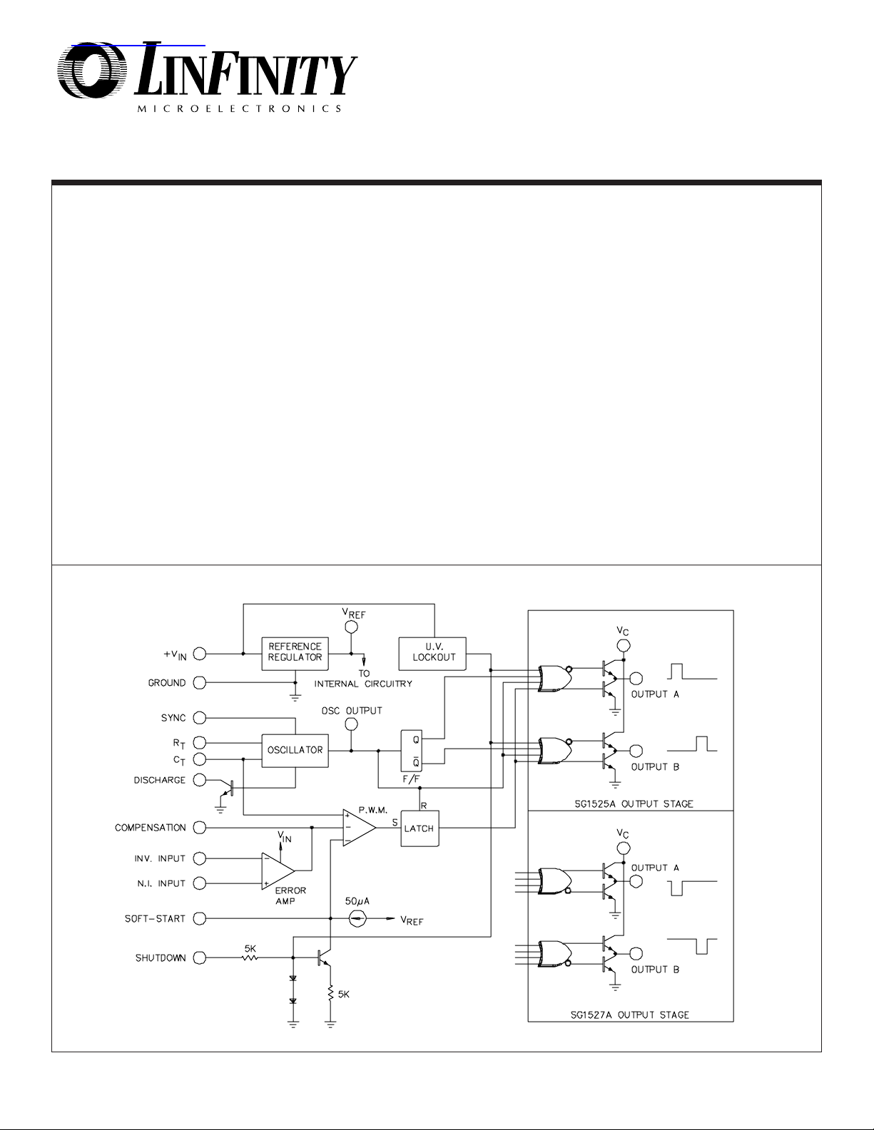
The SG1525A/1527A series of pulse width modulator integrated circuits are
designed to offer improved performance and lower external parts count when used
to implement all types of switching power supplies. The on-chip +5.1 volt reference
is trimmed to ±1% initial accuracy and the input common-mode range of the error
amplifier includes the reference voltage, eliminating external potentiometers and
divider resistors. A Sync input to the oscillator allows multiple units to be slaved
together, or a single unit to be synchronized to an external system clock. A single
resistor between the C
adjustment. These devices also feature built-in soft-start circuitry with only a timing
capacitor required externally. A Shutdown pin controls both the soft-start circuitry
and the output stages, providing instantaneous turn-off with soft-start recycle for
slow turn-on. These functions are also controlled by an undervoltage lockout which
keeps the outputs off and the soft-start capacitor discharged for input voltages less
than that required for normal operation. Another unique feature of these PWM
circuits is a latch following the comparator. Once a PWM pulse has been terminated
for any reason, the outputs will remain off for the duration of the period. The latch
is reset with each clock pulse. The output stages are totem-pole designs capable
of sourcing or sinking in excess of 200mA. The SG1525A output stage features
NOR logic, giving a LOW output for an OFF state. The SG1527A utilizes OR logic
which results in a HIGH output level when OFF.
pin and the Discharge pin provides a wide range of deadtime
T
BLOCK DIAGRAM
FEATURES
••
• 8V to 35V operation
••
••
• 5.1V reference trimmed to ±1%
••
••
• 100Hz to 500KHz oscillator range
••
••
• Separate oscillator sync terminal
••
••
• Adjustable deadtime control
••
••
• Internal soft-start
••
••
• Input undervoltage lockout
••
••
• Latching P.W.M. to prevent multiple
••
pulses
••
• Dual source/sink output drivers
••
HIGH RELIABILITY FEATURES
- SG1525A, SG1527A
♦♦
♦ Available to MIL-STD-883B
♦♦
♦♦
♦ MIL-M38510/12602BEA - JAN1525AJ
♦♦
♦♦
♦ MIL-M38510/12604BEA - JAN1527AJ
♦♦
♦♦
♦ Radiation data available
♦♦
♦♦
♦ LMI level "S" processing available
♦♦
11/91 Rev 1.3 10/96 LINFINITY Microelectronics Inc.
Copyright 1996 11861 Western Avenue
1 (714) 898-8121
∞ ∞
∞ Garden Grove, CA 92841
∞ ∞
∞∞
∞ FAX: (714) 893-2570
∞∞
ABSOLUTE MAXIMUM RATINGS (Note 1)
Supply Voltage (+VIN) .......................................................
Collector Supply Voltage (V
Logic Inputs .......................................................
Analog Inputs .......................................................
) ...........................................
C
-0.3V to 5.5V
-0.3V to V
Output Current, Source or Sink ...................................
Reference Load Current ...............................................
Note 1. Values beyond which damage may occur.
THERMAL DATA
J Package:
Thermal ResistanceThermal Resistance-
DW Package:
Thermal ResistanceThermal Resistance-
L Package:
Thermal ResistanceThermal Resistance-
N Package:
Thermal ResistanceThermal Resistance-
Junction to Case, θ
Junction to Ambient, θ
Junction to Case, θ
Junction to Ambient, θ
Junction to Case, θ
Junction to Ambient, θ
Junction to Case, θ
Junction to Ambient, θ
JC
JC
JC
JC
.................. 30°C/W
.............. 80°C/W
JA
.................. 40°C/W
............. 95°C/W
JA
.................. 35°C/W
........... 120°C/W
JA
................... 40°C/W
............. 65°C/W
JA
40V
40V
500mA
50mA
SG1525A/SG1527A SERIES
Oscillator Charging Current ............................................
Operating Junction Temperature Range
Hermetic (J, L Packages) .....................................
IN
Plastic (N, DW Packages ) .......................................
Storage Temperature Range ..........................
Lead Temperature (Soldering, 10 seconds) .................
Note A. Junction Temperature Calculation: TJ = TA + (PD x θJA).
Note B. The above numbers for
θJC are maximums for the limiting
thermal resistance of the package in a standard mounting configuration. The θ
guidelines for the thermal performance of the device/pc-
numbers are meant to be
JA
board system. All of the above assume no ambient
airflow.
5mA
150°C
150°C
-65°C to 150°C
300°C
RECOMMENDED OPERATING CONDITIONS (Note 2)
Input Voltage (+VIN) ................................................
Collector Voltage (V
Sink/Source Load Current (steady state) .............
) ..........................................
C
Sink/Source Load Current (peak) .........................
Reference Load Current ........................................
Oscillator Frequency Range .......................
100Hz to 350KHz
Oscillator Timing Resistor (RT) ........................
Note 2: Range over which the device is functional.
8V to 35V
4.5V to 35V
0 to 100mA
0 to 400mA
0 to 20mA
2KΩ to 150KΩ
Deadtime Resistor Range (R
Maximum Shutdown Source Impedance .........................
Oscillator Timing Capacitor (C
Operating Ambient Temperature Range
) .............................
D
) ...................
T
SG1525A/SG1527A ....................................
SG2525A/SG2527A ......................................
SG3525A/SG3527A .........................................
0Ω to 500Ω
5KΩ
0.001µF to 0.1µF
-55°C to 125°C
-25°C to 85°C
0°C to 70°C
ELECTRICAL CHARACTERISTICS
(Unless otherwise specified, these specifications apply over the operating ambient temperatures for SG1525A/SG1527A with -55° C ≤ TA ≤ 125°C,
SG2525A/SG2527A with -25°C ≤ TA ≤ 85°C, SG3525A/SG3527A with 0°C ≤ TA ≤ 70°C, and +VIN = 20V. Low duty cycle pulse testing techniques are
used which maintains junction and case temperatures equal to the ambient temperature.)
SG1525A/2525A
SG1527A/2527A
Min. Typ. Max. Min. Typ. Max.
Reference Section
5.15
5.10
Output Voltage
Line Regulation
Load Regulation
Temperature Stability
(Note 3)
Total Output Voltage Range (Note 3)
Short Circuit Current
Output Noise Voltage
(Note 3)
Long Term Stability (Note 3)
Note 3. These parameters, although guaranteed over the recommended operating conditions, are not 100% tested in production.
Note 4. F
Note 5. Applies to SG1525A/2525A/3525A only, due to polarity of output pulses.
= 40KHz (RT = 3.6KΩ, CT = 0.01µF, RD = 0Ω)
OSC
TJ = 25°C
V
= 8V to 35V
IN
= 0 to 20mA
I
L
Over Operating Temperature Range
Over Line, Load and Temperature
V
= 0V, TJ = 25°C
REF
10Hz ≤ f ≤ 10KHz, T
= 125°C
T
J
= 25°C
J
5.05
5.00
10
20
20
80
40
20
30
50
50
5.20
100
200
50
SG3525A
SG3527A
5.00
4.95
5.10
10
20
20
80
40
20
5.20
30
50
50
5.25
100
200
50
UnitsTest ConditionsParameter
V
mV
mV
mV
V
mA
µVrms
mV/khr
11/91 Rev 1.3 10/96 LINFINITY Microelectronics Inc.
Copyright 1996 11861 Western Avenue
2 (714) 898-8121
∞ ∞
∞ Garden Grove, CA 92841
∞ ∞
∞∞
∞ FAX: (714) 893-2570
∞∞
ELECTRICAL CHARACTERISTICS (continued)
SG1525A/SG1527A SERIES
SG1525A/2525A
SG1527A/2527A UnitsTest ConditionsParameter
Min. Typ. Max. Min. Typ. Max.
Oscillator Section
Initial Accuracy
Voltage Stability
Temperature Stability
Minimum Frequency (Note 3)
Maximum Frequency (Note 3)
Current Mirror
Clock Amplitude
Clock Width
Sync Threshold
Sync Input Current
Error Amplifier Section (V
Input Offset Voltage
(Note 4)
(Note 3)
= 5.1V)
CM
TJ = 25°C
V
= 8V to 35V
IN
MIN ≤ T
R
R
I
RT
T
≤ MAX
J
= 150KΩ, CT = 0.1µF
T
= 2KΩ, CT = 1nF
T
= 2mA
= 25°C
J
Sync Voltage = 3.5V
37.6
350
1.7
3.0
0.3
1.2
40
±0.3
±3
2.0
3.5
0.5
2.0
1.0
0.5
Input Bias Current
Input Offset Current
DC Open Loop Gain
Gain-Bandwidth Product
Output Low Level
Output High Level
Common Mode Rejection
Supply Voltage Rejection
(Note 3)
R
≥10MΩ, TJ = 25°C
L
= 0dB, TJ = 25°C
A
V
V
= 1.5V to 5.2V
CM
V
= 8V to 35V
IN
60
1
3.8
60
50
75
0.2
5.6
75
60
P.W.M. Comparator Section
V
Minimum Duty Cycle
Maximum Duty Cycle
Input Threshold
(Note 4)
Input Bias Current
= 0.6V
COMP
V
= 3.6V
COMP
Zero Duty Cycle
Maximum Duty Cycle
45
0.6
49
0.9
3.3
.05
Soft-Start Section
50
Soft Start Current
Soft Start Voltage
Shutdown Input Current
Output Drivers Section
Output High Level
Output Low Level
Undervoltage Lockout
Collector Leakage
(Note 5)
Rise Time
Fall Time
Shutdown Delay
(Note 3)
V
SHUTDOWN
V
SHUTDOWN
V
(each transistor, VC = 20V)
SHUTDOWN
I
SOURCE
I
SOURCE
I
SINK
I
SINK
V
COMP
V
C
C
C
V
SD
= 0V
= 2V
= 2.5V
= 20mA
= 100mA
= 20mA
= 100mA
and VSS = High
= 35V
= 1nF, TJ = 25°C
L
= 1nF, TJ = 25°C
L
= 3V, CS = 0, TJ = 25°C
25
18
17
0.4
0.4
19
18
0.2
1.0
6
100
50
0.2
Total Standby Current
Standby Current VIN = 35V mA20142014
SG3525A
SG3527A
KHz
42.4
40
37.6
42.4
%
±2
350
1.7
3.0
0.3
1.2
60
1
3.8
60
50
45
0.6
25 50
18
17
6
±1
±3
2.0
3.5
0.5
2.0
1.0
2
1
75
2
0.2
5.6
75
60
49
0.9
3.3
.05
0.4
0.4
19
18
0.2
1.0
7
100
50
0.2
±6
150
2.2
1.0
2.8
2.5
10
10
1
0.5
0
3.6
2.0
80
0.6
1.0
0.4
2.2
8
200
600
300
0.5
%
Hz
KHz
mA
V
µs
V
mA
mV
µA
µA
dB
MHz
V
V
dB
dB
%
%
V
V
µA
µA
V
mA
V
V
V
V
V
µA
ns
ns
µs
±1
±6
150
2.2
1.0
2.8
2.5
5
1
10
1
2
0.5
0
3.6
2.0
80
0.6
1.0
0.4
2.2
7
8
200
600
300
0.5
11/91 Rev 1.3 10/96 LINFINITY Microelectronics Inc.
Copyright 1996 11861 Western Avenue
3 (714) 898-8121
∞ ∞
∞ Garden Grove, CA 92841
∞ ∞
∞∞
∞ FAX: (714) 893-2570
∞∞

OSCILLATOR SECTION
SG1525A/SG1527A SERIES
FIGURE 1 - OSCILLATOR SCHEMATIC
FIGURE 2 - OSCILLATOR CHARGE TIME VS. RT AND C
T
FIGURE 3 - OSCILLATOR DISCHARGE TIME VS. RD AND C
T
ERROR AMPLIFIER SECTION
FIGURE 4 - ERROR AMPLIFIER
11/91 Rev 1.3 10/96 LINFINITY Microelectronics Inc.
Copyright 1996 11861 Western Avenue
4 (714) 898-8121
FIGURE 5 - ERROR AMPLIFIER OPEN-LOOP
FREQUENCY RESPONSE
∞ ∞
∞ Garden Grove, CA 92841
∞ ∞
∞∞
∞ FAX: (714) 893-2570
∞∞

OUTPUT SECTION
APPLICATION INFORMATION
SG1525A/SG1527A SERIES
FIGURE 7 - OUTPUT SATURATION CHARACTERISTICSFIGURE 6 -OUTPUT CIRCUIT (½ Circuit Shown)
For single-ended supplies, the driver outputs are grounded. The
terminal is switched to ground by the totem-pole source
V
C
transistors on alternate oscillator cycles.
The low source impedance of the output drivers provides rapid
charging of power FET input capacitance while minimizing external components.
11/91 Rev 1.3 10/96 LINFINITY Microelectronics Inc.
Copyright 1996 11861 Western Avenue
In conventional push-pull bipolar designs, forward base drive is
controlled by R1 - R3 . Rapid turn-off times for the power devices
are achieved with speed-up capacitors C
and C2 .
1
Low power transformers can be driven directly by the SG1525A.
Automatic reset occurs during deadtime, when both ends of the
primary winding are switched to ground.
∞ ∞
∞ Garden Grove, CA 92841
∞ ∞
5 (714) 898-8121
∞∞
∞ FAX: (714) 893-2570
∞∞
APPLICATION INFORMATION (continued)
SHUTDOWN OPTIONS
SG1525A/SG1527A SERIES
1. Use an external transistor or open-collector comparator to pull
down on the Comp terminal. This will set the PWM latch turning
off both outputs. If the shutdown signal is momentary, pulseby-pulse protection can be accomplished as the PWM latch will
be reset with each clock pulse.
2. The same results can be accomplished by pulling down on the
Soft-Start terminal with the difference that on this pin, shutdown
will not affect the amplifier compensation network but must
discharge any Soft-Start capacitor.
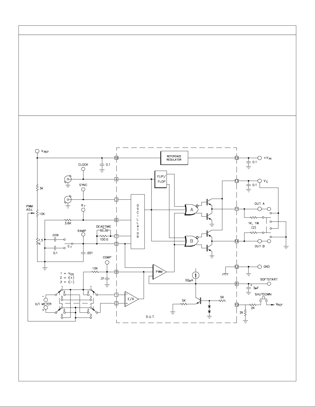
SG1525A/1527A LAB TEST FIXTURE
3. Apply a positive-going signal to the Shutdown terminal. This
will provide most rapid shutdown of the outputs but will not
immediately set the PWM latch if there is a Soft-Start capacitor.
This capacitor will discharge but with a current of approximately twice the charging current.
4. The shutdown terminal can be used to set the PWM latch on
a pulse-by-pulse basis if there is no external capacitance on
Soft-Start terminal. Slow turn-on may still be accomplished by
applying an external capacitor, blocking diode, and charging
resistor to the comp terminal. (See SG1524 Application Note).
11/91 Rev 1.3 10/96 LINFINITY Microelectronics Inc.
Copyright 1996 11861 Western Avenue
6 (714) 898-8121
∞ ∞
∞ Garden Grove, CA 92841
∞ ∞
∞∞
∞ FAX: (714) 893-2570
∞∞

SG1525A/SG1527A SERIES
CONNECTION DIAGRAMS & ORDERING INFORMATION (See Notes Below)
16-PIN CERAMIC DIP
J - PACKAGE
16-PIN PLASTIC DIP
N - PACKAGE
16-PIN WIDE BODY
PLASTIC S.O.I.C.
DW - PACKAGE
Part No.Package
Ambient
Temperature Range
SG1525AJ/883B -55°C to 125°C
JAN1525AJ -55°C to 125°C
SG1525AJ/DESC -55°C to 125°C
SG1525AJ -55°C to 125°C
SG2525AJ -25°C to 85°C
SG3525AJ 0°C to 70°C
SG1527AJ/883B -55°C to 125°C
JAN1527AJ -55°C to 125°C
SG1527AJ/DESC -55°C to 125°C
SG1527AJ -55°C to 125°C
SG2527AJ -25°C to 85°C
SG3527AJ 0°C to 70°C
SG2525AN -25°C to 85°C
SG3525AN 0°C to 70°C
SG2527AN -25°C to 85°C
SG3527AN 0°C to 70°C
SG2525ADW -25°C to 85°C
SG3525ADW 0°C to 70°C
SG2527ADW -25°C to 85°C
SG3527ADW 0°C to 70°C
Connection Diagram
INV. INPUT
N.I. INPUT
SYNC
OSC. OUTPUT
INV. INPUT
N.I. INPUT
OSC. OUTPUT
DISCHARGE
SOFT-START
DISCHARGE
SYNC
C
T
R
T
C
T
R
T
1
2
3
4
5
6
7
8
11516
2
3
4
5
6
7
8
14
13
12
11
10
9
16
15
14
13
12
11
10
V
REF
+V
IN
OUTPUT B
V
C
GROUND
OUTPUT A
SHUTDOWN
COMPENSATIONSOFT-START
9
V
REF
+V
IN
OUTPUT B
V
C
GROUND
OUTPUT A
SHUTDOWN
COMPENSATION
20-PIN CERAMIC
LEADLESS CHIP CARRIER
L- PACKAGE
SG1525AL/883B -55°C to 125°C
SG1525AL -55°C to 125°C
SG1527AL/883B -55°C to 125°C
SG1527AL -55°C to 125°C
Note 1. Contact factory for JAN and DESC product availablity.
2. All packages are viewed from the top.
1. N.C.
2. INV. INPUT
3. N.I. INPUT
4. SYNC
5. OSC. OUTPUT
6. N.C.
7. C
T
8. R
T
9. DISCHARGE
10. SOFT-START
4
5
6
7
8
321
9 11121310
20 19
11. N.C.
12. COMP.
18
13. SHUTDOWN
14. OUTPUT A
17
15. GROUND
16
16. N.C.
15
17. V
14
18. OUTPUT B
19. +V
20. V
C
IN
REF
11/91 Rev 1.3 10/96 LINFINITY Microelectronics Inc.
Copyright 1996 11861 Western Avenue
7 (714) 898-8121
∞ ∞
∞ Garden Grove, CA 92841
∞ ∞
∞∞
∞ FAX: (714) 893-2570
∞∞
 Loading...