LINFINITY SG29125, SG125A Service Manual

查询SG29125供应商
SG29125/125A
LOW DROPOUT DUAL REGULATOR
DESCRIPTION
The SG29125/125A is a dual 12V/5V positive voltage regulator. One output is a high
current (up to 1000 mA) regulator that can be turned on or off by a high impedance low
current TTL compatible switch. The second or standby output remains on regardless.
The on/off switch not only shuts off the high current output but actually puts the IC in
a micropower mode making possible a low quiescent current. This unique characteristic coupled with an extremely low dropout, (.55V for output current of 10mA) makes
the SG29125/125A well suited for power systems that require standby memory. The
SG29125/125A includes other features which were originally designed for automotive
applications. These include protection from reverse battery installations and double
battery jumps. The high current regulator has overvoltage shutdown to protect both
the internal circuitry and the load during line transients, such as load dump (60V). In
addition, the high current regulator design also has built-in protection for short circuit
and thermal overload. During these fault conditions of the primary regulator the
standby regulator will continue to power its load.
The SG29125 is the 12 volt, ±5% version of a family of dual regulators with a standby
output voltage of 5V. Other high current outputs of 5 and 8.2 volts are available. Also
available is the SG29125A which offers an improved output voltage tolerance of ±2%.
They are available in the plastic TO-220 power package and are designed to function
over the automotive ambient temperature range of -40°C to 85°C.
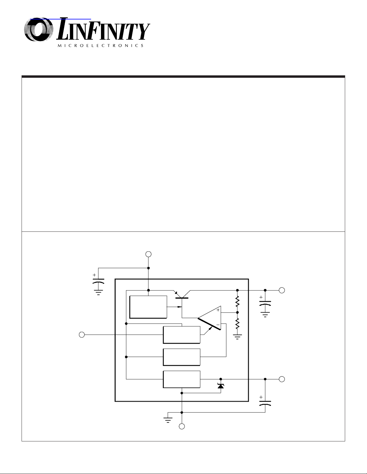
TYPICAL APPLICATION CIRCUIT
C1
*
0.1µF
INPUT VOLTAGE
1
OVERVOLTAGE
THERMAL
SHUTDOWN
SG29125/125A
* Required if regulator is located far from power
** Required for stability. May be increased without
FEATURES
••
• 2% Internally Trimmed Output
••
••
• Two regulated outputs
••
••
• Output current in excess of
••
1000mA
••
• Low quiescent current standby
••
regulator
••
• Input-output differential less than
••
0.6V at 0.5A
••
• Reverse battery protection
••
••
• 60V load dump protection
••
••
• -50V reverse transient protection
••
••
• Short circuit protection
••
••
• Internal thermal overload protec-
••
tion
••
• Available in plastic TO-220
••
••
• ON/OFF switch for high current
••
output
supply filter.
bound. Capacitor must be rated to operate at the
minimum temperature expected for the regulator
system.
2
C2
10µF
**
OUTPUT VOLTAGE
(12V, 1000mA)
ON/OFF SWITCH
(for output voltage only)
12/90 Rev 1.1 2/94 LINFINITY Microelectronics Inc.
Copyright 1994 11861 Western Avenue
4
REGULATOR
BIAS
1.23V
REFERENCE
5V STANDBY
REGULATOR
3
GROUND
5.6V
5
C3**
10µF
1 (714) 898-8121
STANDBY OUTPUT
(5V, 50mA)
∞ ∞
∞ Garden Grove, CA 92841
∞ ∞
∞∞
∞ FAX: (714) 893-2570
∞∞

ABSOLUTE MAXIMUM RATINGS Note 1. Exceeding these values may destroy this part.
Input Voltage (VIN) Operating ..............................................
Input Voltage (V
ON/OFF Switch .......................................................
) Overvoltage Transient ..............
IN
-15V to 60V
-0.3V to V
26V
Storage Temperature Range (T
Operating Junction Temperature (T
IN
THERMAL DATA
SG29125/125A
) ..................
STG
) ..............................
J
-65°C to 150°C
150°C
P Package:
Thermal Resistance-
Junction to Case, θ
................ 4.0°C/W*
JT
Thermal Resistance-Junction to Ambient, θJA.............. 55°C/W
θθ
* =
θJT (Junction to Tab)
θθ
Note A. Junction Temperature Calculation: TJ = TA + (PD x θJA).
Note B. The above numbers for
θJC are maximums for the limiting
thermal resistance of the package in a standard mounting configuration. The θ
guidelines for the thermal performance of the device/pc-
numbers are meant to be
JA
board system. All of the above assume no ambient
airflow.
RECOMMENDED OPERATING CONDITIONS (Note 2 & 3)
Input Voltage (VIN) .....................................................
13V to 26V
ON/OFF Threshold Voltage
(V
Low Level, V
High Level, V
Load Current V
Maximum Line Transient (Load Dump) V
Input Capacitor (V
Note 2. Range over which the device is functional.
Note 3. During 60V load dump, VSB shall not be less than 4.75V at I
is OFF) ..................................
IL
OUT
(V
is ON) ....................................
IH
OUT
(with adequate heatsinking) .....
OUT
to GND) ...................................
IN
SB
5 to 1000mA
≤ 6V .......
0.8V max.
2.0V min.
60V max.
0.1 µF min.
Reverse Polarity D.C. Input Voltage (V
(V
≥ -0.6V, 16Ω load) ...........................................
O
Reverse Polarity Transient Input Voltage (V
(1% duty cycle, T ≤ 100ms, V
Output Capacitor with ESR of 1Ω max.
to GND & VSBto GND) ...................................
(V
OUT
Operating Ambient Temperature Range (T
SG29125/125A ...............................................
= 10mA.
OUT
O
)
IN
)
IN
≥ -9V, 16Ω load) ...
)
A
-40°C to 85°C
-15V max.
-50V max.
10µF min.
ELECTRICAL CHARACTERISTICS (Unless otherwise specified, these specifications apply for the operating ambient temperature of
= 25°C, VIN = 14V, IO = 500mA for V
T
A
maintains junction and case temperatures equal to the ambient temperature.)
Voltage Output (V
Output Voltage
OUT
(Note 4)
) Section
Line Regulation
Load Regulation
Output Impedance
Quiescent Current
Output Noise Voltage
Long Term Stability
Ripple Rejection
Dropout Voltage
Current Limit
Maximum Operational Input Voltage
Maximum Line Transient
ON/OFF Switch (I
ON/OFF Switch (I
)
IH
)
IL
and 10mA for VSB and are for DC characteristics only. Low duty cycle pulse testing techniques are used which
OUT
Test ConditionsParameter
13V ≤ V
SG29125
≤ 26V, IO ≤ 1000mA, -40°C ≤ TA ≤ 85°C
IN
SG29125A
13V ≤ V
13V ≤ V
5mA ≤ I
500mA
≤ 10mA, No Load on Standby
I
O
I
= 500mA, No Load on Standby
O
= 750mA, No Load on Standby
I
O
I
= 220mA, ISB = 10mA, VIN = V
O
10Hz - 100kHz
F
O
= 500mA
I
O
I
=1000mA
O
≤ 16V, IO = 5mA
IN
≤ 26V, IO = 5mA
IN
≤ 1000mA
O
and 10mA
DC
= 120Hz
, 100Hz - 10kHz
RMS
Double Battery
V
≤ 13V
O
= 10mA, Pin 4 = 2.4V
I
O
I
= 10mA, Pin 4 = 0.4V
O
- 200mV
OUT
SG29125/125A
Typ.
Min. Max.
11.2
12
12.8
11.75
12
10
10
12.25
4
25
50
50
200
2
40
100
90
15
25
100
20
66
0.45
0.6
.0.7
1.0
26.5
60
1.8
31
70
1.2
2.5
10
-10
Units
V
V
mV
mV
mV
mΩ
mA
mA
mA
mA
µV
mV/1000hr
dB
V
V
A
V
V
µA
µA
RMS
12/90 Rev 1.1 2/94 LINFINITY Microelectronics Inc.
Copyright 1994 11861 Western Avenue
2 (714) 898-8121
∞ ∞
∞ Garden Grove, CA 92841
∞ ∞
∞∞
∞ FAX: (714) 893-2570
∞∞
 Loading...