

SG120
NEGATIVE FIXED VOLTAGE REGULATOR
DESCRIPTION
The SG120 series of negative regulators offer self-contained, fixed-voltage
capability with up to 1.5A of load current. With a variety of output voltages and four
package options this regulator series is an optimum complement to the SG7800A/
7800/120 line of three terminal regulators.
All protective features of thermal shutdown, current limiting, and safe-area control
have been designed into these units and since these regulators require only a
single output capacitor or a capacitor and 5mA minimum load for satisfactory
performance, ease of application is assured.
Although designed as fixed-voltage regulators, the output voltage can be increased through the use of a simple voltage divider. The low quiescent drain
current of the device insures good regulation when this method is used, especially
for the SG120 series. Utilizing an improved Bandgap reference design, problems
have been eliminated that are normally associated with the zener diode references, such as drift in output voltage and large changes in the line and load
regulation
These devices are available in TO-257 (hermetically sealed TO-220), both
isolated and non-isolated), TO-3, TO-39 and TO-66 power packages.
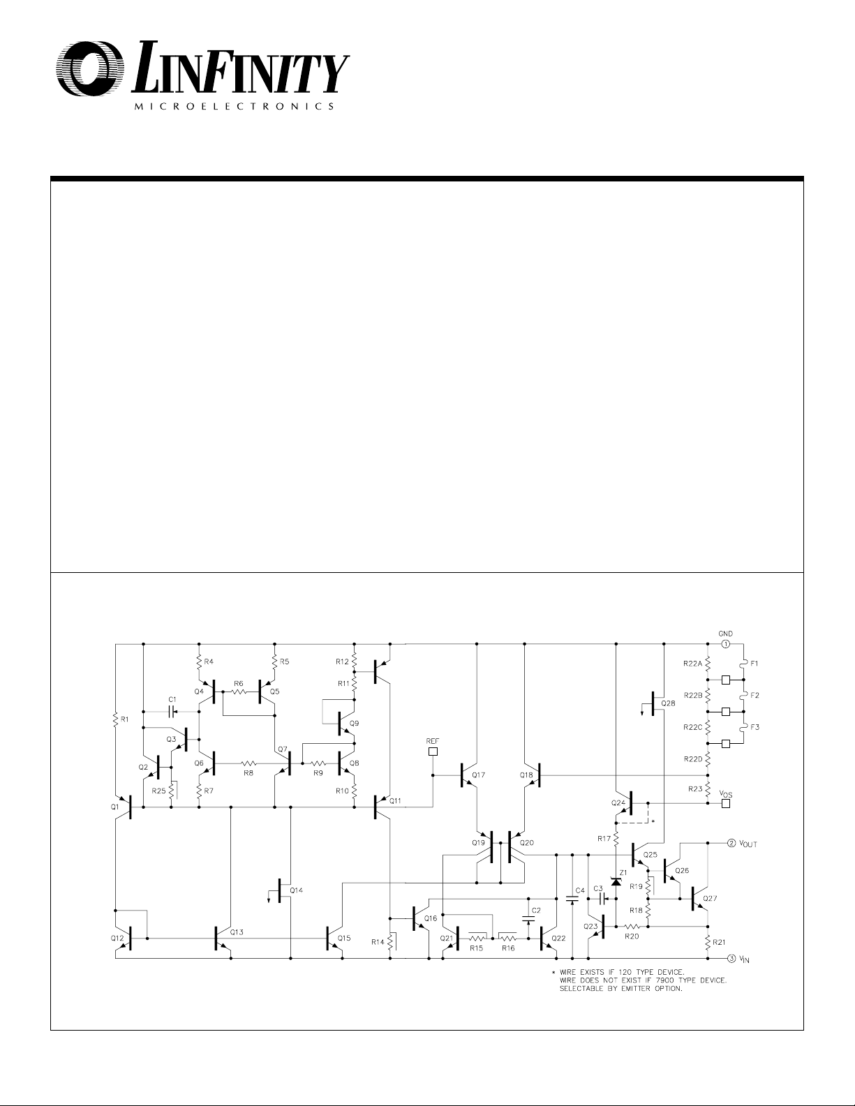
SCHEMATIC DIAGRAM
FEATURES
••
• Output current to 1.5A
••
••
• Excellent line and load regulation
••
••
• Foldback current limiting
••
••
• Thermal overload protection
••
••
• Voltages available: -5V, -12V, -15V
••
••
• Voltages Not Recommended For New
••
Designs: -5.2V, -8V, -18V, -20V
••
• Contact factory for other voltage
••
options
HIGH RELIABILITY FEATURES
- SG120
♦♦
♦ Available to MIL-STD - 883
♦♦
♦♦
♦ Radiation data available
♦♦
♦♦
♦ LMI level "S" processing available
♦♦
11/91 Rev 1.4 6/97 LINFINITY Microelectronics Inc.
Copyright 1997 11861 Western Avenue
1 (714) 898-8121
∞ ∞
∞ Garden Grove, CA 92841
∞ ∞
∞∞
∞ FAX: (714) 893-2570
∞∞
SG120
ABSOLUTE MAXIMUM RATINGS (Note 1)
Device Input Voltage Differential
Output Voltage Input Voltage (Output shorted to ground)
-5V -35V 35V
-5.2V -35V 35V
-8V -35V 35V
-12V -35V 35V
-15V -40V 35V
-18V -40V 35V
-20V -40V 35V
NEGATIVE REGULATOR
Operating Junction Temperature
Hermetic (K, R, IG - Packages) ...................................
Note 1. Values beyond which damage may occur.
150°C
THERMAL DATA
K Package:
Thermal ResistanceThermal Resistance-
R Package:
Junction to Case, θ
Junction to Ambient, θ
................. 3.0°C/W
JC
............... 35°C/W
JA
Thermal Resistance-Junction to Case, θJC................. 5.0°C/W
Thermal Resistance-Junction to Ambient, θJA.............. 40°C/W
T Package:
Thermal Resistance-Junction to Case, θJC.................. 15°C/W
Thermal Resistance-Junction to Ambient, θJA............ 120°C/W
IG Package:
Thermal Resistance-Junction to Case, θJC................. 3.5°C/W
Thermal Resistance-Junction to Ambient, θJA.............. 42°C/W
L Package:
Thermal Resistance-Junction to Case, θJC.................. 35°C/W
Thermal Resistance-Junction to Ambient, θJA............ 120°C/W
RECOMMENDED OPERATING CONDITIONS (Note 2)
Operating Junction Temperature Range:
SG120 ...........................................................
-55°C to 150°C
Storage Temperature Range ...........................
-65°C to 150°C
Lead Temperature (Soldering, 10 Seconds) .................
Note A. Junction Temperature Calculation: TJ = TA + (PD x θJA).
Note B. The above numbers for θ
resistance of the package in a standard mounting configuration.
The θJA numbers are meant to be guidelines for the thermal
performance of the device/pc-board system. All of the above
assume no ambient airflow.
are maximums for the limiting thermal
JC
300°C
Note 2. Range over which the device is functional.
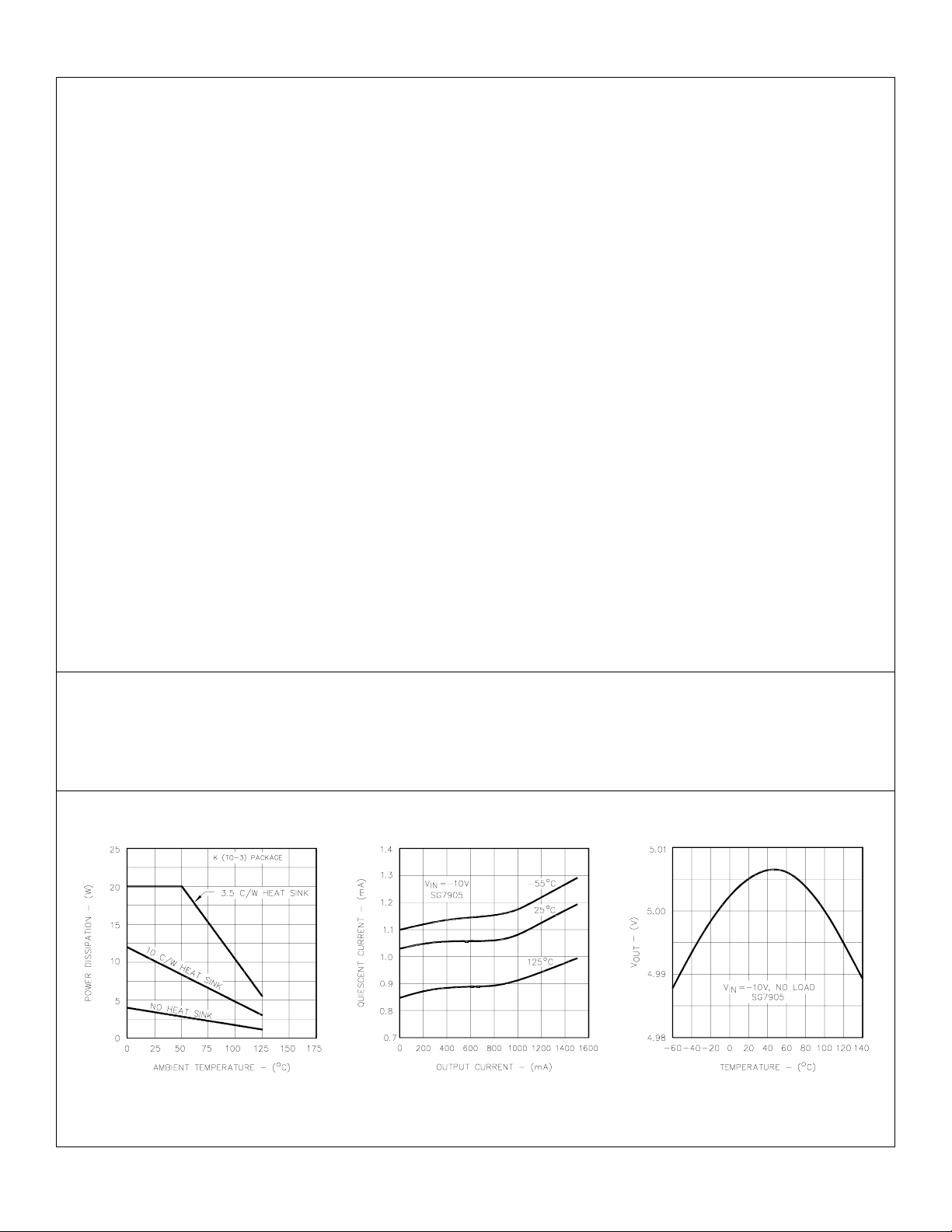
CHARACTERISTIC CURVES
FIGURE 1.
MAXIMUM AVERAGE POWER DISSIPATION
11/91 Rev 1.4 6/97 LINFINITY Microelectronics Inc.
Copyright 1997 11861 Western Avenue
FIGURE 2.
QUIESCENT CURRENT VS. LOAD
2 (714) 898-8121
FIGURE 3.
TEMPERATURE COEFFICIENT
∞ ∞
∞ Garden Grove, CA 92841
∞ ∞
∞∞
∞ FAX: (714) 893-2570
∞∞
SG120
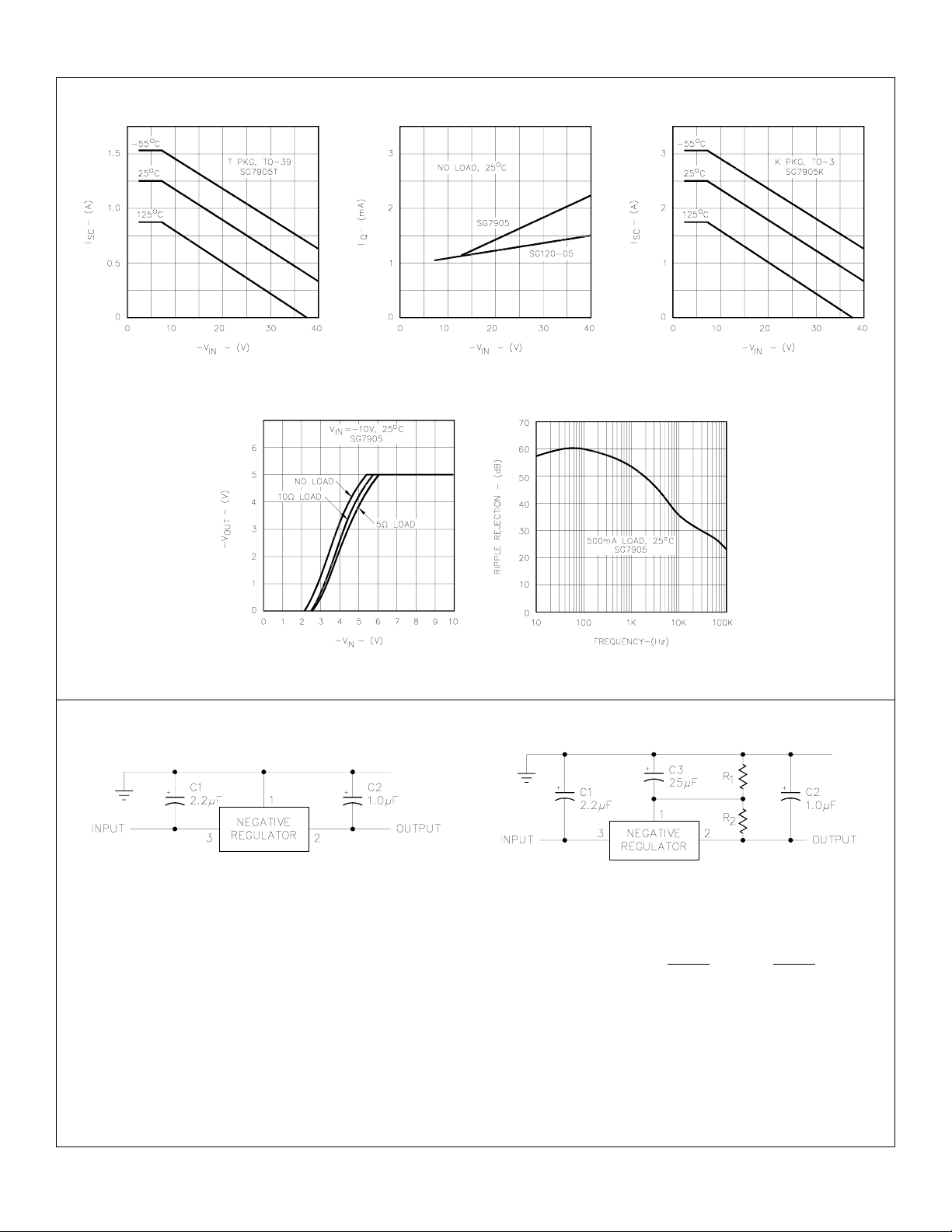
CHARACTERISTIC CURVES (continued)
NEGATIVE REGULATOR
FIGURE 4.
SHORTCIRCUIT CURRENT VS. V
APPLICATIONS
IN
FIGURE 7.
DROPOUT CHARACTERISTICS
FIGURE 5.
QUIESCENT CURRENT VS. V
FIGURE 6.
IN
FIGURE 8.
RIPPLE REJECTION VS. FREQUENCY
SHORT CIRCUIT CURRENT VS. V
IN
FIGURE 9 - FIXED OUTPUT REGULATOR
NOTE: 1. C1 is required only if regulator is separated from rectifier filter.
2. Both C1 and C2 should be low E.S.R. types such as solid
tantalum. If aluminum electrolitics are used, at least 10 times
values shown should be selected.
3. If large output capacities are used, the regulators must be
NOTE: C3 optional for improved transient response and ripple
FIGURE 10 - CIRCUIT FOR INCREASING OUTPUT VOLTAGE
rejection.
R1 + R
2
V
= V (REGULATOR)
OUT
R
1
R2 =
V(REG)
15mA
protected from momentary input shorts. A high current diode
from output to input will suffice.
11/91 Rev 1.4 6/97 LINFINITY Microelectronics Inc.
Copyright 1997 11861 Western Avenue
3 (714) 898-8121
∞ ∞
∞ Garden Grove, CA 92841
∞ ∞
∞∞
∞ FAX: (714) 893-2570
∞∞

SG120
-5.0V & -5.2V NEGATIVE REGULATOR
ELECTRICAL CHARACTERISTICS (Note 1)
SG120-05
(Unless otherwise specified, these specifications apply over full operating ambient temperatures for SG120-05 with -55°C ≤ TA ≤ 150°C, and
V
= -10V, IO = 5mA, CIN = 2mF, C
IN
to the ambient temperature.)
Parameter
Output Voltage
Line Regulation (Note 1)
Load Regulation (Note 1)
Total Output Voltage
Tolerance
Quiescent Current
Quiescent Current Change
Dropout Voltage
Peak Output Current
Short Circuit Current
Ripple Rejection
Output Noise Voltage (rms)
Long Term Stability
Thermal Shutdown
= 1.0mF. Low duty cycle pulse testing techniques are used which maintains junction and case temperature equal
OUT
Test Conditions
TJ = 25°C
V
= -7V to -25V, TJ = 25°C
IN
Power Pkgs: IO = 5mA to 1.5A, TJ = 25°C
T - Pkg: IO = 5mA to 500mA, TJ = 25°C
SG120-05
Min. Typ. Max.
-5.1
-5.0
-4.9
10
50
30
VIN = -7.5V to -25V
Power Pkgs: I
T - Pkg: I
VIN = -7V to -25V
= 5mA to 1.5A, P ≤ 20W
O
= 5mA to 500mA, P ≤ 2W
O
With Line: VIN = -7V to -25V, TJ = 25°C
-4.8
-4.8
-5.0
-5.2
0.4
-5.2
-5.0
With Load: TJ = 25°C
Power Pkgs: IO = 5mA to 1.5A
T - Pkg: IO = 5mA to 500mA
0.4
0.4
∆VO = 100mV, TJ = 25°C
2.3
1.5
0.5
54
1.1
3.3
1.4
1.2
0.6
25
20
175
Power Pkgs: IO = 1.0A, T - Pkg: IO = 500mA
Power Pkgs: TJ = 25°C
T - Pkg: TJ = 25°C
Power Pkgs: VIN = -35V, TJ = 25°C
T - Pkg: VIN = -35V, TJ = 25°C
∆VIN = 10V, f = 120Hz, TJ = 25°C
f = 10Hz to 100KHz (Note 2)
1000hrs. at TJ = 125°C
IO = 5mA
25
75
50
80
Units
V
mV
mV
mV
V
V
2
mA
mA
mA
mA
V
A
A
A
A
dB
µV/V
mV
°C
SG120-5.2
(Unless otherwise specified, these specifications apply over full operating ambient temperatures for SG120-5.2 with -55°C ≤ TA ≤ 150°C, and
VIN = -10V, IO = 5mA, CIN = 2mF, C
to the ambient temperature.)
Parameter
Output Voltage
Line Regulation (Note 1)
Load Regulation (Note 1)
Total Output Voltage
Tolerance
Quiescent Current
Quiescent Current Change
= 1.0mF. Low duty cycle pulse testing techniques are used which maintains junction and case temperature equal
OUT
Test Conditions
TJ = 25°C
VIN = -7.2V to -25V, TJ = 25°C
Power Pkgs: IO = 5mA to 1.5A, TJ = 25°C
T - Pkg: IO = 5mA to 500mA, TJ = 25°C
SG120-5.2
Min. Typ. Max.
-5.1
-5.2
-5.3
15
25
50
75
30
50
VIN = -7.7V to -25V
-5.0
-5.2
-5.2
-5.4
-5.4
2
0.4
Power Pkgs: IO = 5mA to 1.5A, P ≤ 20W
T - Pkg: IO = 5mA to 500mA, P ≤ 2W
VIN = -7.2V to -25V
With Line: VIN = -7.2V to -25V, TJ = 25°C
-5.0
With Load: TJ = 25°C
1.1
25
20
175
0.4
0.4
2.3
3.3
1.4
1.2
0.6
80
Dropout Voltage
Peak Output Current
Short Circuit Current
Ripple Rejection
Output Noise Voltage (rms)
Long Term Stability
Thermal Shutdown
Power Pkgs: IO = 5mA to 1.5A
T - Pkg: IO = 5mA to 500mA
∆VO = 100mV, TJ = 25°C
Power Pkgs: IO = 1.5A, T - Pkg: IO = 500mA
Power Pkgs: TJ = 25°C
T - Pkg: TJ = 25°C
Power Pkgs: VIN = -35V, TJ = 25°C
T - Pkg: VIN = -35V, TJ = 25°C
∆VIN = 10V, f = 120Hz, TJ = 25°C
f = 10Hz to 100KHz (Note 2)
1000hrs. at TJ = 125°C
IO = 5mA
1.5
0.5
54
Units
V
mV
mV
mV
V
V
mA
mA
mA
mA
V
A
A
A
A
dB
µV/V
mV
°C
Note 1. All regulation tests are made at constant junction temperature with low duty cycle testing.
2. This test is guaranteed but is not tested in production.
11/91 Rev 1.4 6/97 LINFINITY Microelectronics Inc.
Copyright 1997 11861 Western Avenue
4 (714) 898-8121
∞ ∞
∞ Garden Grove, CA 92841
∞ ∞
∞∞
∞ FAX: (714) 893-2570
∞∞

SG120
-8V & -12V NEGATIVE REGULATOR
ELECTRICAL CHARACTERISTICS (Note 1)
SG120-08
(Unless otherwise specified, these specifications apply over full operating ambient temperatures for SG120-08 with -55°C ≤ TA ≤ 150°C, and
VIN = -14V, IO = 5mA, CIN = 1.0mF, C
to the ambient temperature.)
Output Voltage
Line Regulation (Note 1)
Load Regulation (Note 1)
Total Output Voltage
Tolerance
Quiescent Current
Quiescent Current Change
Dropout Voltage
Peak Output Current
Short Circuit Current
Ripple Rejection
Output Noise Voltage (rms)
Long Term Stability
Thermal Shutdown
= 1.0mF. Low duty cycle pulse testing techniques are used which maintains junction and case temperature equal
OUT
Test Conditions
= 25°C
T
J
VIN = -10.5V to -25V, TJ = 25°C
Power Pkgs: IO = 5mA to 1.5A, TJ = 25°C
T - Pkg: IO = 5mA to 500mA, TJ = 25°C
= -10.5V to -25V
V
IN
Power Pkgs: I
T - Pkg: IO = 5mA to 500mA, P ≤ 2W
= 5mA to 1.5A, P ≤ 20W
O
Min.
-7.8
-7.65
-7.65
SG120-8
Typ. Max.
-8.0
10
20
10
-8.00
-8.00
-8.2
-8.35
-8.35
VIN = -10.5V to -25V
With Line: VIN = -10.5V to -25V, TJ = 25°C
With Load: T
Power Pkgs: I
T - Pkg: IO = 5mA to 500mA
= 25°C
J
= 5mA to 1.5A
O
0.4
0.4
0.4
∆VO = 100mV, TJ = 25°C
1.1
Power Pkgs: IO = 1.0A, T - Pkg: IO = 500mA
Power Pkgs: TJ = 25°C
T - Pkg: TJ = 25°C
Power Pkgs: VIN = -35V, TJ = 25°C
T - Pkg: VIN = -35V, TJ = 25°C
∆VIN = 10V, f = 120Hz, TJ = 25°C
f = 10Hz to 100KHz (Note 2)
1000hrs. at TJ = 125°C
IO = 5mA
1.5
0.5
54
2.3
3.3
1.4
1.2
0.6
25
32
175
25
80
25
80
UnitsParameter
V
mV
mV
mV
V
V
2
mA
mA
mA
mA
V
A
A
A
A
dB
µV/V
mV
°C
SG120-12
(Unless otherwise specified, these specifications apply over full operating ambient temperatures for SG120-12 with -55°C ≤ TA ≤ 150°C, and
VIN = -17V, IO = 5mA, CIN = 2.0mF, C
to the ambient temperature.)
Parameter
Output Voltage
Line Regulation
(Note 1)
Load Regulation (Note 1)
Total Output Voltage
Tolerance
Quiescent Current
Quiescent Current Change
= 1.0mF. Low duty cycle pulse testing techniques are used which maintains junction and case temperature equal
OUT
Test Conditions
T
= 25°C
J
VIN = -14V to -32V, TJ = 25°C
Power Pkgs: IO = 5mA to 1.0A, TJ = 25°C
T - Pkg: IO = 5mA to 500mA, TJ = 25°C
SG120-12
Min. Typ.
-11.7
-12.0
4
30
10
Max.
-12.3
10
80
25
VIN = -14.5V to -32V
-11.5
-11.5
-12.0
-12.0
2
-12.5
-12.5
4
0.4
Power Pkgs: IO = 5mA to 1.0A, P ≤ 20W
T - Pkg: IO = 5mA to 500mA, P ≤ 2W
VIN = -14V to -32V
With Line: VIN = -14V to -32V, TJ = 25°C
With Load: TJ = 25°C
Dropout Voltage
Peak Output Current
Short Circuit Current
Ripple Rejection
Output Noise Voltage (rms)
Long Term Stability
Thermal Shutdown
Power Pkgs: IO = 5mA to 1.0A
T - Pkg: IO = 5mA to 500mA
∆VO = 100mV, TJ = 25°C
Power Pkgs: IO = 1.0A, T - Pkg: IO = 500mA
Power Pkgs: TJ = 25°C
T - Pkg: TJ = 25°C
Power Pkgs: VIN = -35V, TJ = 25°C
T - Pkg: VIN = -35V, TJ = 25°C
∆VIN = 10V, f = 120Hz, TJ = 25°C
f = 10Hz to 100KHz (Note 2)
1000hrs. at TJ = 125°C
IO = 5mA
1.5
0.5
56
175
1.1
25
48
0.4
0.4
2.3
3.3
1.4
1.2
0.6
80
Units
V
mV
mV
mV
V
V
mA
mA
mA
mA
V
A
A
A
A
dB
µV/V
mV
°C
Note 1. All regulation tests are made at constant junction temperature with low duty cycle testing.
2. This test is guaranteed but is not tested in production.
11/91 Rev 1.4 6/97 LINFINITY Microelectronics Inc.
Copyright 1997 11861 Western Avenue
5 (714) 898-8121
∞ ∞
∞ Garden Grove, CA 92841
∞ ∞
∞∞
∞ FAX: (714) 893-2570
∞∞

SG120
-15V & -18V NEGATIVE REGULATOR
ELECTRICAL CHARTACTERISTICS (Note 1)
SG120-15
(Unless otherwise specified, these specifications apply over full operating ambient temperatures for SG120-15 with -55°C ≤ TA ≤ 150°C, and
VIN = -20V, IO = 5mA, CIN = 2.0mF, C
to the ambient temperature.)
Parameter
Output Voltage
Line Regulation (Note 1)
Load Regulation (Note 1)
Total Output Voltage
Tolerance
Quiescent Current
Quiescent Current Change
Dropout Voltage
Peak Output Current
Short Circuit Current
Ripple Rejection
Output Noise Voltage (rms)
Long Term Stability
Thermal Shutdown
= 1.0mF. Low duty cycle pulse testing techniques are used which maintains junction and case temperature equal
OUT
Test Conditions
TJ = 25°C
VIN = -17V to -35V, TJ = 25°C
Power Pkgs: IO = 5mA to 1.0A, TJ = 25°C
T - Pkg: IO = 5mA to 500mA, TJ = 25°C
= -17.5V to -35V
V
IN
Power Pkgs: I
T - Pkg: IO = 5mA to 500mA, P ≤ 2W
= 5mA to 1.0A, P ≤ 20W
O
VIN = -17V to -35V
SG120-15
Min. Typ. Max.
-14.7
-15.0
-15.3
5
30
10
-14.5
-15.0
-15.5
-14.5
-15.0
-15.5
2
With Line: VIN = -17V to -35V, TJ = 25°C
With Load: T
Power Pkgs: I
T - Pkg: IO = 5mA to 500mA
= 25°C
J
= 5mA to 1.0A
O
∆VO = 100mV, TJ = 25°C
Power Pkgs: IO = 1.0A, T - Pkg: IO = 500mA
Power Pkgs: TJ = 25°C
T - Pkg: TJ = 25°C
1.1
1.5
0.5
Power Pkgs: VIN = -35V, TJ = 25°C
T - Pkg: VIN = -35V, TJ = 25°C
∆VIN = 10V, f = 120Hz, TJ = 25°C
f = 10Hz to 100KHz (Note 2)
1000hrs. at TJ = 125°C
IO = 5mA
56
25
60
175
10
80
25
4
0.4
0.4
0.4
2.3
3.3
1.4
1.2
0.6
80
Units
V
mV
mV
mV
V
V
mA
mA
mA
mA
V
A
A
A
A
dB
µV/V
mV
°C
SG120-18
(Unless otherwise specified, these specifications apply over full operating ambient temperatures for SG120-18 with -55°C ≤ TA ≤ 150°C, and
VIN = -27V, IO = 5mA, CIN = 2.0mF, C
to the ambient temperature.)
Parameter
Output Voltage
Line Regulation (Note 1)
Load Regulation (Note 1)
Total Output Voltage
Tolerance
Quiescent Current
Quiescent Current Change
= 1.0mF. Low duty cycle pulse testing techniques are used which maintains junction and case temperature equal
OUT
Test Conditions
T
= 25°C
J
VIN = -21V to -33V, TJ = 25°C
Power Pkgs: IO = 5mA to 1.0A, TJ = 25°C
T - Pkg: IO = 5mA to 500mA, TJ = 25°C
SG120-18
Min. Typ. Max.
-17.6
-18.0
-18.4
5
10
30
80
10
25
VIN = -22V to -33V
-17.4
-18.0
-18.0
2
-18.6
-18.6
4
0.4
Power Pkgs: IO = 5mA to 1.0A, P ≤ 20W
T - Pkg: IO = 5mA to 500mA, P ≤ 2W
VIN = -21V to -33V
With Line: VIN = -21V to -33V, TJ = 25°C
-17.4
With Load: TJ = 25°C
1.1
25
72
175
0.4
0.4
2.3
3.3
1.4
1.2
0.6
Dropout Voltage
Peak Output Current
Short Circuit Current
Ripple Rejection
Output Noise Voltage (rms)
Long Term Stability
Thermal Shutdown
Power Pkgs: IO = 5mA to 1.0A
T - Pkg: IO = 5mA to 500mA
∆VO = 100mV, TJ = 25°C
Power Pkgs: IO = 1.0A, T - Pkg: IO = 500mA
Power Pkgs: TJ = 25°C
T - Pkg: TJ = 25°C
Power Pkgs: VIN = -35V, TJ = 25°C
T - Pkg: VIN = -35V, TJ = 25°C
∆VIN = 10V, f = 120Hz, TJ = 25°C
f = 10Hz to 100KHz (Note 2)
1000hrs. at TJ = 125°C
IO = 5mA
1.5
0.5
56
Units
V
mV
mV
mV
V
V
mA
mA
mA
mA
V
A
A
A
A
dB
µV/V
mV
°C
Note 1. All regulation tests are made at constant junction temperature with low duty cycle testing.
2. This test is guaranteed but is not tested in production.
11/91 Rev 1.4 6/97 LINFINITY Microelectronics Inc.
Copyright 1997 11861 Western Avenue
6 (714) 898-8121
∞ ∞
∞ Garden Grove, CA 92841
∞ ∞
∞∞
∞ FAX: (714) 893-2570
∞∞

SG120
-20V NEGATIVE REGULATOR
ELECTRICAL CHATRACTERISTICS (Note 1)
SG120-20
(Unless otherwise specified, these specifications apply over full operating ambient temperatures for SG120-20 with -55°C ≤ TA ≤ 150°C, and
VIN = -29V, IO = 5mA, CIN = 2.0mF, C
to the ambient temperature.)
Parameter
Output Voltage
Line Regulation (Note 1)
Load Regulation (Note 1)
Total Output Voltage
Tolerance
Quiescent Current
Quiescent Current Change
Dropout Voltage
Peak Output Current
Short Circuit Current
Ripple Rejection
Output Noise Voltage (rms)
Long Term Stability
Thermal Shutdown
= 1.0mF. Low duty cycle pulse testing techniques are used which maintains junction and case temperature equal
OUT
Test Conditions
TJ = 25°C
VIN = -23V to -35V, TJ = 25°C
Power Pkgs: IO = 5mA to 1.0A, TJ = 25°C
T - Pkg: IO = 5mA to 500mA, TJ = 25°C
= -24V to -35V
V
IN
Power Pkgs: I
T - Pkg: IO = 5mA to 500mA, P ≤ 2W
= 5mA to 1.0A, P ≤ 20W
O
VIN = -23V to -35V
SG120-20
Min. Typ. Max.
-20.5
-20.0
-19.5
5
30
10
-20.7
-20.0
-19.3
-20.7
-20.0
-19.3
2
With Line: VIN = -23V to -35V, TJ = 25°C
With Load: T
Power Pkgs: I
T - Pkg: IO = 5mA to 500mA
= 25°C
J
= 5mA to 1.0A
O
∆VO = 100mV, TJ = 25°C
Power Pkgs: IO = 1.0A, T - Pkg: IO = 500mA
Power Pkgs: TJ = 25°C
T - Pkg: TJ = 25°C
1.1
1.5
0.5
Power Pkgs: VIN = -35V, TJ = 25°C
T - Pkg: VIN = -35V, TJ = 25°C
∆VIN = 10V, f = 120Hz, TJ = 25°C
f = 10Hz to 100KHz (Note 2)
1000hrs. at TJ = 125°C
IO = 5mA
56
25
80
175
10
80
25
4
0.4
0.4
0.4
2.3
3.3
1.4
1.2
0.6
80
Units
V
mV
mV
mV
V
V
mA
mA
mA
mA
V
A
A
A
A
dB
µV/V
mV
°C
Note 1. All regulation tests are made at constant junction temperature with low duty cycle testing.
2. This test is guaranteed but is not tested in production.
11/91 Rev 1.4 6/97 LINFINITY Microelectronics Inc.
Copyright 1997 11861 Western Avenue
7 (714) 898-8121
∞ ∞
∞ Garden Grove, CA 92841
∞ ∞
∞∞
∞ FAX: (714) 893-2570
∞∞

SG120
CONNECTION DIAGRAMS & ORDERING INFORMATION (See Notes Below)
NEGATIVE REGULATOR
3-TERMINAL TO-3
METAL CAN
K-PACKAGE
3-TERMINAL TO-66
METAL CAN
R-PACKAGE
3-PIN TO-39 METAL CAN
T-PACKAGE
Part No.Package
Ambient
Temperature Range
SG120-XXK/883B -55°C to 125°C
SG120-XXK -55°C to 125°C
SG120-XXR/883B -55°C to 125°C
SG120-XXR -55°C to 125°C
SG120-XXT/883B -55°C to 125°C
SG120-XXT -55°C to 125°C
Connection Diagram
GROUND
V
GROUND
V
GROUND
V
OUT
OUT
OUT
CASE IS V
1
2
CASE IS V
IN
1
2
CASE IS V
IN
1
V
32
IN
IN
3-PIN HERMETIC TO-257
IG-PACKAGE (Isolated)
20-PIN CERAMIC (LCC)
LEADLESS CHIP CARRIER
L- PACKAGE
SG120-XXIG/883B -55°C to 125°C
SG120-XXIG -55°C to 125°C
SG120-XXL/883B -55°C to 125°C
SG120-XXL -55°C to 125°C
(Note 4) 1. N.C.
2. V
IN
3. N.C.
4. V
OUT
5. V
OUT
6. N.C.
7. V
OUT
8. N.C.
9. N.C.
10. N.C.
SENSE
3212019
4
5
6
7
8
9
10 11 12 13
V
OUT
V
IN
GROUND
18
17
16
15
14
11. N.C.
12. N.C.
13. N.C.
14. N.C.
15. GND
16. N.C.
17. GND
18. N.C.
19. N.C.
20. V
IN
Note 1. Contact factory for JAN and DESC product availability.
2. All parts are viewed from the top.
3. "XX" to be replaced by output voltage of specific fixed regulator.
4. Some products will be available in leadless chip carrier (LCC) and hermetic flat pack (F). Consult factory for price and availability
11/91 Rev 1.4 6/97 LINFINITY Microelectronics Inc.
Copyright 1997 11861 Western Avenue
8 (714) 898-8121
∞ ∞
∞ Garden Grove, CA 92841
∞ ∞
∞∞
∞ FAX: (714) 893-2570
∞∞

WWW.ALLDATASHEET.COM
Copyright © Each Manufacturing Company.
All Datasheets cannot be modified without permission.
This datasheet has been download from :
www.AllDataSheet.com
100% Free DataSheet Search Site.
Free Download.
No Register.
Fast Search System.
www.AllDataSheet.com
 Loading...