

V
T
查询LX8580供应商
LX8580
7A V
ERY LOW DROPOUT POSITIVE ADJUSTABLE REGULATOR
T HE I NFINITE P OWER OF I NNOVATION
DESCRIPTION KEY FEATURES
The LX8580 is a high-performance, very
low dropout voltage regulator, designed for
use with advanced microprocessors. This
product can be used with separate voltage
supplies for the control and power sections,
allowing a power section dropout voltage
as low as 100mV. The LX8580 can also be
used in a single voltage supply configuration,
with a dropout performance similar to that
of the LX8584 (1.3V at 7A).
The LX8580 is supplied in a five-
terminal TO-220 package, which allows the
NOTE: For current data & package dimensions, visit our web site: http://www.linfinity.com.
implementation of remote (Kelvin) voltage
sensing. This sensing compensates for
output voltage variations due to load
changes and resistive voltage drops in
connectors and board traces. Typical load
regulation measured at the sense pin is less
than 1mV for a load current step of 7mA
to 7A.
The LX8580 is ideal for generating a
secondary 2 - 2.5V low voltage supply on a
motherboard where a 3.3V supply is already
available.
PRODUCT HIGHLIGHT
SPECIAL CAPABILITIES OF THE LX8580 TO ALLOW 44%
SMALLER LDO THERMAL DISSIPATION
P RODUCTION DATA SHEET
■■
■ Low Dropout, 800mV Max. at 7A
■■
Output Current in Dual Supply Mode
■■
■ Fast Transient Response
■■
■■
■ Remote Sensing
■■
! 1mV Load Regulation
! Adjustable Output
! No Supply Sequencing Problems in Dual
Supply Mode
APPLICATIONS
■ Microprocessor Supplies
■ 3.3V to 2.5V Processor Power Supplies
■ High-Current Regulators
■ Post Regulators for Switching Supplies
CTRL
³ V
+ 1.3V Max
OUT
4
V
CTRL
OUTPUT
3
V
OU
LX8580
5
V
V
PWR
³ V
OUT
+ V
DROPOUT
PWR
SENSE
ADJUST
2
R
V
= V
OUT
REF
B
1 + + I
R
A
x R
ADJ
B
R
B
PACKAGE ORDER INFORMATION
T
(°C)
A
0 to 125 0.1V - 0.8V LX8580-00CP LX8580-00CDD
Dropout
Voltage
Plastic TO-220
P
5-pin
1
R
A
LOAD
Plastic TO-263
DD
5-pin
Copyright © 1999
Rev. 1.0 11/99
L INF INITY MICROELECTRONICS INC.
11861 WESTERN A VENUE, GARDEN G ROVE, CA. 92841, 714-898-8121, FAX: 714-893-2570
1
LX8580
V
PRODUCT DATABOOK 1996/1997
7A V
ERY LOW DROPOUT POSITIVE ADJUSTABLE REGULATOR
P RODUCTION DATA SHEET
ABSOLUTE MAXIMUM RATINGS (Note 1)
Power Dissipation ......................................................................................Internally Limited
V
Input Voltage ........................................................................................................... 7V
PWR
Input Voltage ......................................................................................................... 13V
V
CTRL
Operating Junction Temperature
Plastic (P Package) ................................................................................................ 150°C
Storage Temperature Range ...................................................................... -65°C to 150°C
Lead Temperature (Soldering, 10 seconds) ............................................................. 300°C
Note 1. Exceeding these ratings could cause damage to the device. All voltages are with respect
to Ground. Currents are positive into, negative out of the specified terminal.
THERMAL DATA
P PACKAGE:
THERMAL RESISTANCE-JUNCTION TO TAB,
THERMAL RESISTANCE-JUNCTION TO AMBIENT,
DD PACKAGE:
THERMAL RESISTANCE-JUNCTION TO TAB,
THERMAL RESISTANCE-JUNCTION TO AMBIENT,
Junction Temperature Calculation: TJ = TA + (PD x θJA).
The θJA numbers are guidelines for the thermal performance of the device/pc-board system.
All of the above assume no ambient airflow.
θθ
θ
θθ
JT
θθ
θ
θθ
JA
θθ
θ
θθ
JT
θθ
θ
θθ
JA
3.0°C/W
60°C/W
3.0°C/W
60°C/W
PACKAGE PIN OUTS
TAB IS OUTPUT
5
1
P PACKAGE
(Top View)
TAB IS OUTPUT
5
4
3
2
1
DD PACKAGE
(Top View)
V
PWR
V
CTRL
OUTPUT
ADJUST
SENSE
V
PWR
V
CTRL
OUTPUT
ADJUST
SENSE
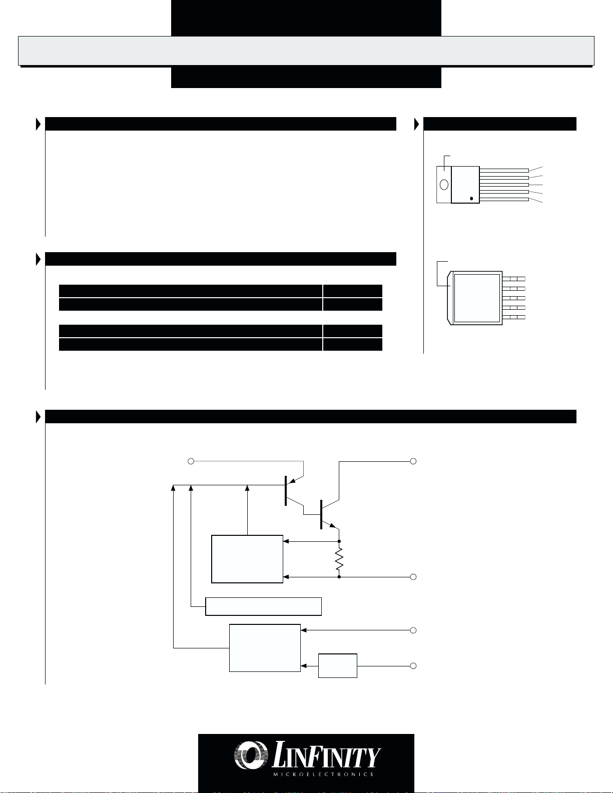
BLOCK DIAGRAM
Control
CTRL
Power
V
PWR
Current
Limiting
Amplifier
OUTPUT
Thermal Overload
Voltage
SENSE
Regulation
Amplifier
V
REF
ADJUST
2
Copyright © 1999
Rev. 1.0 11/99

PRODUCT DATABOOK 1996/1997
LX8580
7A V
ERY LOW DROPOUT POSITIVE ADJUSTABLE REGULATOR
P RODUCTION DATA SHEET
ELECTRICAL CHARACTERISTICS
(Unless otherwise specified, these specifications apply over the operating ambient temperatures 0°C ≤ TA ≤ 125°C. Low duty cycle pulse testing
techniques are used which maintains junction and case temperatures equal to the ambient temperature.)
Parameter
Reference Voltage V
Line Regulation ∆V
Load Regulation
Thermal Regulation
Thermal Resistance R
Ripple Rejection V
Control Pin Current (Note 3) I
Adjust Pin Current I
Current Limit I
Dropout Voltage (Control Section) V
Minimum V
(V
- V
PWR
Dropout Voltage (Power Section) V
Minimum V
(V
- V
PWR
(V
= 0) V
ADJ
Minimum Load Current V
Note 2. Dropout is caused by either minimum control voltage (V
the output voltage. The specifications represent the minimum input/output voltage required to maintain 1% regulation.
(Note 2) V
CTRL
)V
OUT
(Note 2) V
PWR
)V
OUT
Symbol
REF
(VIN)
REF
∆V
(I
)
REF
OUT
∆V
(Pwr) 30ms Pulse
OUT
θJT
CTRL
ADJ
θ(MAX)VCTRL
- V
CTRL
OUTVPWR
- V
PWR
OUTVCTRL
Test Conditions
V
= 2.75V, V
CTRL
V
= 2.7V to 6V,
CTRL
V
= 2.7V to 6V,
CTRL
V
= 2.5V to 12V, V
CTRL
= 2.5V to 12V, V
V
CTRL
V
= 2.75V, V
CTRL
Control Circuitry/Power Transistor
= V
CTRL
PWR
V
= 2.75V, V
CTRL
V
= 2.75V, V
CTRL
V
= 2.75V, V
CTRL
V
= 2.75V, V
CTRL
V
= 2.75V, V
CTRL
= 2.75V, V
= 2.05V, I
= 2.05V, I
PWR
= 2.05V, I
PWR
V
= 2.05V, I
PWR
V
= 2.05V, I
PWR
= 2.75V, I
= 2.75V, I
CTRL
= 2.75V, I
CTRL
= 2.75V, I
CTRL
V
= 2.75V, I
CTRL
V
= 2.75V, I
CTRL
V
= 2.75V, I
CTRL
= 5V, V
CTRL
= 2V, I
PWR
V
PWR
V
PWR
PWR
PWR
= 2.1V, I
PWR
= 3.75V Avg, V
= 2.05V, I
PWR
= 2.05V, I
PWR
= 1.75V, I
PWR
= 2.05V, I
PWR
= 2.05V, I
PWR
= 2.05V, ∆V
PWR
= 100mA
LOAD
= 1A
LOAD
= 2.75A
LOAD
= 4A
LOAD
= 7A
LOAD
= 100mA
LOAD
= 1A
LOAD
= 2.75A
LOAD
= 4A, TJ = 25°C
LOAD
= 4A
LOAD
= 7A, TJ = 25°C
LOAD
= 7A
LOAD
= 3.3V, V
PWR
) or minimum power voltage (V
CTRL
= 10mA, TJ = 25°C
LOAD
= 1.75V to 5.5V, I
= 2.05V to 5.5V, I
= 1.75V to 5.5V, I
= 1.75V to 5.5V, I
= 10mA to 7A (V
LOAD
= 1V
RIPPLE
= 100mA
LOAD
= 4A
LOAD
= 4A
LOAD
= 7A
LOAD
= 0mA (V
LOAD
OUT
= 0V
ADJ
= 10mA to 4A
OUT
= 10mA to 7A
OUT
= 10mA, TJ = 25°C
LOAD
= 10mA
LOAD
, V
= 0V, I
P-P
ADJ
ADJ
= 100mV (V
= 0)
ADJ
= 4A
OUT
= 0)
= 0)
ADJ
). Both parameters are specified with respect to
PWR
Note 3. The control pin current is the drive current required for the output transistor. This current will track output current with roughly a 1:100 ratio.
The minimum value is equal to the quiescent current of the device.
LX8580
Min. Typ. Max.
Units
1.243 1.250 1.257 V
1.237 1.250 1.263 V
1.237 1.250 1.263 V
13mV
26mV
27mV
0.002 0.020 %/W
0.65 2.70 °C/W
60 80 dB
310mA
30 60 mA
33 70 mA
60 120 mA
60 120 µA
7.1 9 A
0.90 1.15 V
1.00 1.15 V
1.05 1.18 V
1.06 1.20 V
1.10 1.30 V
0.05 0.17 V
0.10 0.22 V
0.20 0.38 V
0.30 0.40 V
0.30 0.50 V
0.52 0.62 V
0.56 0.80 V
510mA
Copyright © 1999
Rev. 1.0 11/99
3

LX8580
K
Pin # Description
PRODUCT DATABOOK 1996/1997
7A V
ERY LOW DROPOUT POSITIVE ADJUSTABLE REGULATOR
P RODUCTION DATA SHEET
FUNCTIONAL PIN DESCRIPTION
SENSE 1
ADJUST 2
OUTPUT 3
V
CTRL
V
PWR
5.0V
"Electronic Heatsink"
This pin is the positive side of the reference voltage for the device. With this pin it is possible to Kelvin-sense the output voltage
at load.
This pin is the negative side of the reference voltage for the device. Ripple rejection can be improved by adding a small bypass capacitor
from the Adjust pin to ground. The capacitor value should be selected so that C
and RA is the value of the resistor between the output and sense leads of the LX8580.
This is the power output of the device.
4
This pin is the voltage supply pin for the control circuitry of the device. The current flow into this pin will be about 1% of the output
current. For the device to regulate, the voltage at this pin must be between 1.0V and 1.3V greater than the output voltage.
5
This is the collector of the power section of the LX8580. The output load current is supplied through this pin. For the device to
regulate, the voltage at this pin must be between 0.1V and 0.8V greater than the output voltage (higher output currents require higher
voltages between V
and OUTPUT).
PWR
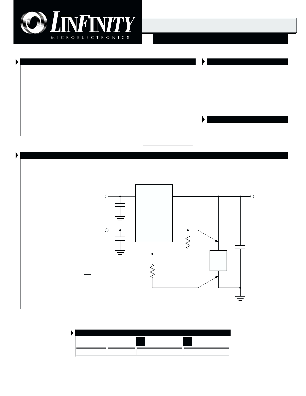
BASIC APPLICATION CIRCUIT
≤ 1 / 2πFRRA , where FR is the ripple frequency
R
Tantalum
4 x 19 2W 5%
(Parallel Connected)
33µF 10V
V
OUT
= 2.775
2.89 (MAX)
2.67 (MIN)
OUTPUT
V
CTRL
LX8580
SENSE
V
0.259
Resistor reduces
thermal load
on LDO heatsink
to 6.9W
PWR
Tantalum
100µF
10V
ADJUST
*Note
1219
1%
1479
1%
LOAD
6000µF
(4X Sanyo 6mV 1500G
6.3V 1500µF)
5A
*Note: For improved transient response, add capacitor as shown (typical 15µF).
PRODUCTION DATA - Information contained in this document is proprietary to LinFinity, and is current as of publication date. This document
may not be modified in any way without the express written consent of LinFinity. Product processing does not necessarily include testing of all
parameters. Linfinity reserves the right to change the configuration and performance of the product and to discontinue product at any time.
4
SYSTEM GROUND
Copyright © 1999
Rev. 1.0 11/99
 Loading...