

查询LX1681供应商
LX1681/1682
VOLTAGE-MODE PWM CONTROLLERS
T HE I NFINITE P OWER OF I NNOVATION
DESCRIPTION KEY FEATURES
The LX1681/1682 are monolithic, pulsewidth modulator controller ICs. They are
designed to implement a flexible, low cost
buck (step-down) regulator supply with minimal external components.
The LX1681 is a non-synchronous con-
troller; the LX1682 has a synchronous driver
for higher efficiency.
The output voltage is adjustable by
means of a resistor divider to set the voltage
between 1.25V and 4.5V.
Short-circuit current limiting can be
implemented without expensive current
sense resistors. Current is sensed using the
voltage drop across the R
— sensing is delayed for 1µs to eliminate
of the MOSFET
DS(ON)
MOSFET ringing errors.
NOTE: For current data & package dimensions, visit our web site: http://www.linfinity.com.
Hiccup-mode fault protection reduces
average power to the power elements during
short-circuit conditions.
Switching frequency is fixed at 200kHz
for optimal cost and space.
Under-voltage lockout and soft-start
for optimal start-up performance. The
LX1681/82 can be disabled by pulling the softstart pin to ground.
Small 8-pin SOIC packaging reduces
board space.
Optimized for 5V-to-3.3V or 5V-to-2.5V
conversion, the LX1681/82 can also be used
for converting 12V to 5V, 3.3V or other
voltages with high efficiency, eliminating the
need for bulky heat sinks.
P RODUCTION DATA SHEET
■ Fixed 200kHz Switching Frequency
■ Constant Frequency Voltage-Mode Control
Requires NO External Compensation
■ Hiccup-Mode Over-Current Protection
■ High Efficiency
■ Output Voltage Set By Resistor Divider
■ Under-Voltage Lockout
■ Soft-Start And Enable
■ Synchronous Rectification (LX1682)
■ Non-Synchronous Rectification (LX1681)
■ Small, 8-pin Surface Mount Package
APPLICATIONS
■ 5V to 3.3V Or Less Buck Regulators
■ FPGA Supplies
■ Microprocessor Chipset Supplies
(e.g. Camino, Whitney, etc.)
■ Rambus® RIMMTM Supplies
■ Hard Disk Drives
■ Computer Add-on Cards
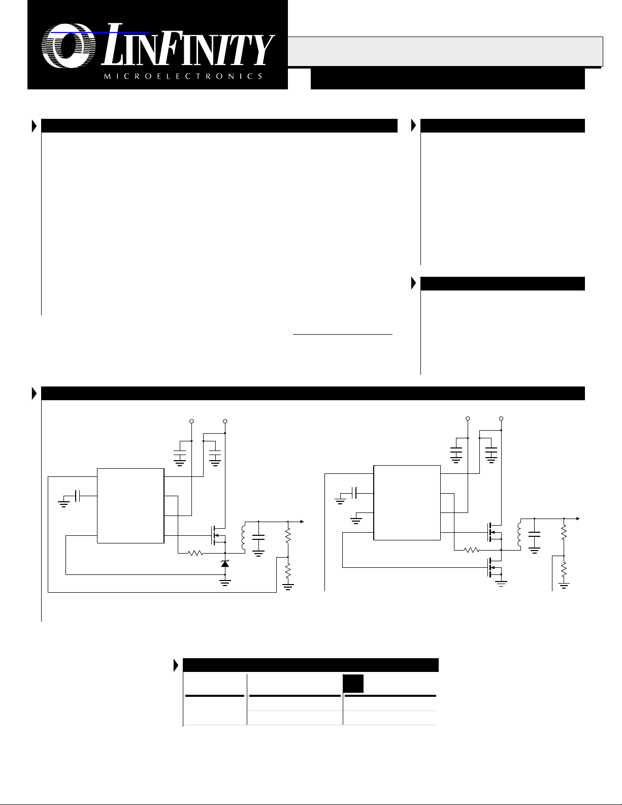
PRODUCT HIGHLIGHT
V
V
CS
V
TDRV
BOOST
12V
C
3
1µF
8
CC
7
6
C1
54
C
SS
0.1µF
V
BOOST
12V
C
3
1µF
1
V
FB
2
SS
LX1681
3
N.C.
GND
V
CS
V
TDRV
8
CC
7
6
C1
IRL3103S
54
R
SET
Q
1
V
IN
5V
C
1
1500µFx3
L
1
5µH
D
2
MBR2545
C
2
1500µF
x3
1
V
C
0.1µF
V
OUT
R
1
R
2
FB
SS
2
SS
LX1682
3
GND
BDRV
LX1681 NON-SYNCHRONOUS CONTROLLER LX1682 SYNCHRONOUS CONTROLLER
PACKAGE ORDER INFORMATION
T
(°C)
A
0 to 70
Output
Non-Synchronous LX1681CDM
Synchronous LX1682CDM
Note: All surface-mount packages are available in Tape & Reel,
append the letter "T" to part number. (i.e. LX1681CDMT)
Plastic SOIC
DM
8-pin
IRL3103S
R
SET
Q
1
V
IN
5V
C
1
1500µFx2
L
1
5µH
Q
2
IRL3103S
C
2
1500µF
x3
V
OUT
R
1
R
2
Copyright © 1999
Rev. 1.0 5/99
L INF INITY MICROELECTRONICS INC.
11861 WESTERN AVENUE, GARDEN GROVE, CA. 92841, 714-898-8121, FAX: 714-893-2570
1
LX1681/1682
PRODUCT DATABOOK 1996/1997
VOLTAGE-MODE PWM CONTROLLERS
P RODUCTION DATA SHEET
ABSOLUTE MAXIMUM RATINGS (Note 1)
PACKAGE PIN OUTS
Supply Voltage (VC1) ............................................................................................18V
Supply Voltage (VCC) .............................................................................................. 7V
Output Drive Peak Current Source (500ns)....................................................... 1.0A
Output Drive Peak Current Sink (500ns)........................................................... 1.0A
Input Voltage (SS/ENABLE Pin) ............................................................. -0.3V to 6V
Operating Junction Temperature .................................................................... 150°C
Storage Temperature Range ........................................................... -65°C to +150°C
Lead Temperature (Soldering, 10 Seconds).................................................... 300°C
Note 1. Exceeding these ratings could cause damage to the device. All voltages are with
respect to Ground. Currents are positive into, negative out of the specified
terminal.
N.C. / GND*
GND / BDRV*
* Pin 3 = N.C. for LX1681, GND for LX1682
Pin 4 = GND for LX1681, BDRV for LX1682
1 8
V
FB
27
SS
36
45
DM PACKAGE
(Top View)
V
CC
CS
V
C1
TDRV
THERMAL DATA
DM PACKAGE:
THERMAL RESISTANCE-JUNCTION TO AMBIENT,
θθ
θ
θθ
JA
165°C/W
Junction Temperature Calculation: TJ = TA + (PD x θJA).
The θJA numbers are guidelines for the thermal performance of the device/pc-board
system. All of the above assume no ambient airflow.
ELECTRICAL CHARACTERISTICS
(
Unless otherwise specified, 4.75V < VCC < 5.25V and 10.8V < VC1 < 13.2V, 0°C ≤ TA ≤ 70°C. Test conditions: VCC = 5V, VC1 = 12V, T = 25°C.
Parameter
Symbol
Test Conditions
LX1681/1682
Min. Typ. Max.
Reference
Reference Voltage V
V
FB
= VFB , TA = 25°C
OUT
V
= VFB , 0°C ≤ TA ≤ 70°C
OUT
1.237 1.25 1.262 V
1.231 1.269 V
Oscillator
Frequency F
Ramp Amplitude V
OSC
RAMP
170 190 230 kHz
1.25 V
Error Amplifier
Input Resistance R
V
OUT
= V
FB
IN
20 kΩ
Current Sense
Current Set I
V
TRIP
Current Sense Delayed T
SETVCS
CSD
= VCC - 0.4V
Reference to V
40 45 µA
CC
-460 -400 -340 mV
1.1 µsec
Output Drivers
Drive Rise Time, Fall Time T
Drive High V
Drive Low V
CL = 3000pF
RF
DHISOURCE
DLISINK
= 20mA, VC1 = 12V
= 20mA, VC1 = 12V
50 ns
10 11 V
0.1 0.2 V
UVLO and Soft-Start (SS)
V
Start-Up Threshold V
CC5
Hysteresis
SS Resistor R
SS Output Enable V
Hiccup Duty Cycle DC
ST
SS
EN
HICCSS
VC1 > 4.0V
= 0.1µF, F
= 100Hz
REQ
4.0 4.25 4.5 V
0.10 V
20 kΩ
0.25 0.3 0.35 V
10 %
Supply Current
V
Dynamic Supply Current I
CC12
Static Supply Current 12V I
5V I
Out Freq = 200kHz, CL = 3000pF, Synch., VSS > 0.3V
CD
VC1VSS
VCCVSS
< 0.3V
< 0.3V
24 28 mA
57mA
10 12 mA
)
Units
PP
2
Copyright © 1999
Rev. 1.0 5/99
PRODUCT DATABOOK 1996/1997
LX1681/1682
VOLTAGE-MODE PWM CONTROLLERS
P RODUCTION DATA SHEET
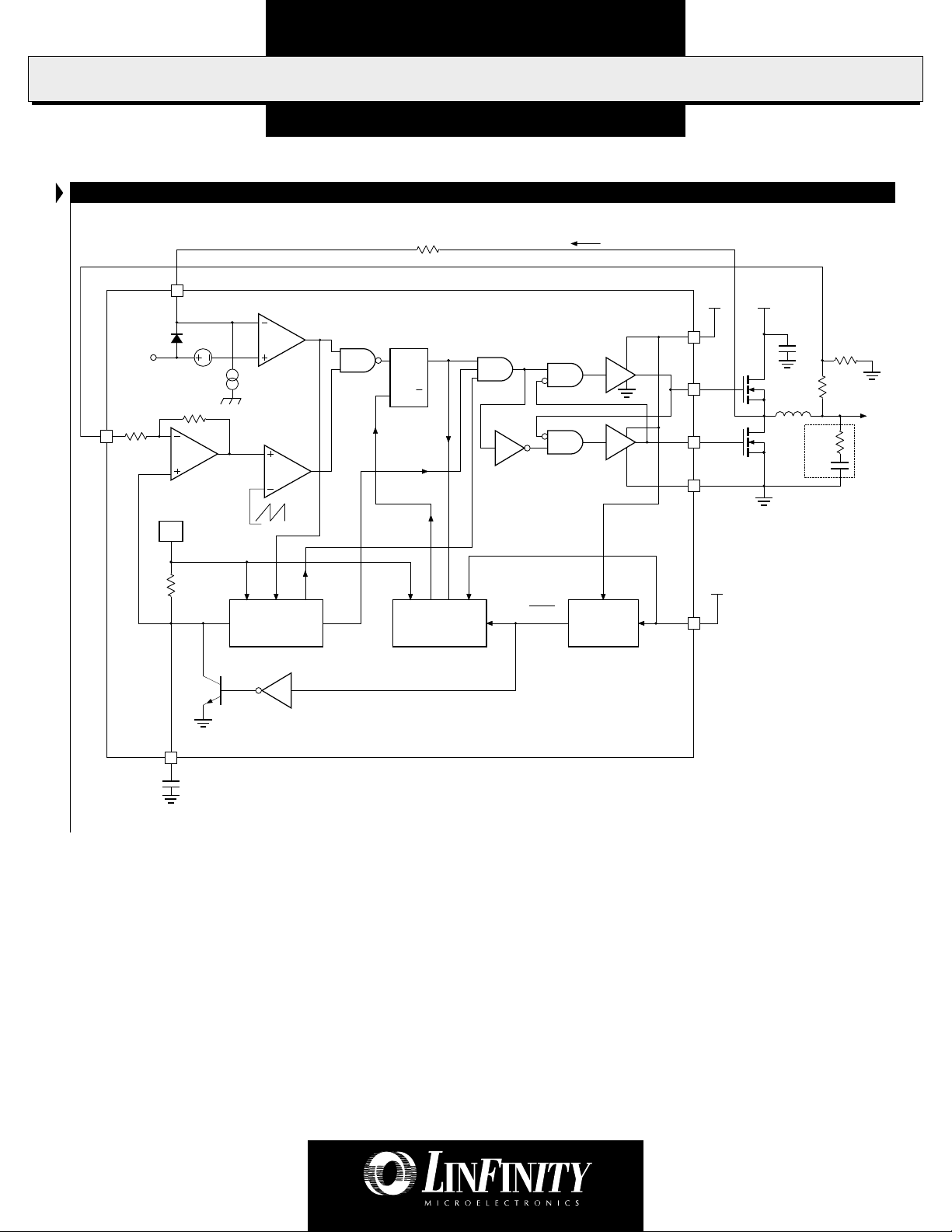
BLOCK DIAGRAM
I
SET
R
SET
CS
7
CS Comp
I
Error
Comp
RESET
PWM
R
Q
SQ
Set
V
RESET
V
TRIP
V
CC
I
SET
320k
20k
1
V
FB
Amplifier/
Compensation
6
5
4
3
+12V
V
C1
TDRV
BDRV
GND
VIN (5V)
C
IN
R
2
R
1
L
V
CORE
ESR
C
OUT
C
SS
V
REF
SS
2
SS/ENABLE
Hiccup
Hiccup
Ramp
UVLO
Oscillator
FIGURE 1 — Block Diagram
UVLO
+5VR
8
V
CC
Copyright © 1999
Rev. 1.0 5/99
3

LX1681/1682
Pin Pin Number
Name Description LX1681 LX1682
V
FB
SS Soft-start and hiccup capacitor pin. During start up the voltage of this pin controls the 2 2
GND Ground for IC 43
TDRV Gate drive for upper MOSFET 5 4
BDRV Gate drive for lower MOSFET 5
V
C1
CS Over-current set. Connect resistor between CS pin and the source of the upper MOSFET to 7 7
V
CC
Voltage feedback — 1.25V reference is connected to a resistor divider to set desired 1 1
output voltage.
output voltage. An internal 20kΩ resistor and the external capacitor set the time constant
for soft-startup. Soft-start does not begin until the supply voltage exceeds the UVLO
threshold. When over-current occurs, this capacitor is used for timing hiccup.
The PWM can be disabled by pulling the SS pin below 0.3V.
Separate supply for MOSFET gate drive. Connect to 12V 6 6
set current-limit point.
IC supply voltage (nominal 5V) and high side drain sense voltage. 8 8
PRODUCT DATABOOK 1996/1997
VOLTAGE-MODE PWM CONTROLLERS
P RODUCTION DATA SHEET
FUNCTIONAL PIN DESCRIPTION
4
Copyright © 1999
Rev. 1.0 5/99

PRODUCT DATABOOK 1996/1997
VOLTAGE-MODE PWM CONTROLLERS
P RODUCTION DATA SHEET
THEORY OF OPERATION
LX1681/1682
GENERAL DESCRIPTION
The LX1681/82 are voltage-mode pulse-width modulation controller integrated circuits. The internal oscillator and ramp
generator frequency is fixed at 200kHz. The devices have
internal compensation, so that no external compensation is
required.
POWER UP and INITIALIZATION
At power up, the LX1681/82 monitors the supply voltage to both
the +5V and the +12V pins (there is no special requirement for
the sequence of the two supplies). Before both supplies reach
their under-voltage lock-out (UVLO) thresholds, the soft-start
(SS) pin is held low to prevent soft-start from beginning; the
oscillator control is disabled and the top MOSFET is kept OFF.
SOFT-START
Once the supplies are above the UVLO threshold, the soft-start
capacitor begins to be charged up by the reference through a
20kΩ internal resistor. The capacitor voltage at the SS pin rises
as a simple RC circuit. The SS pin is connected to the amplifier's
non-inverting input that controls the output voltage. The output
voltage will follow the SS pin voltage if sufficient charging
current is provided to the output capacitor.
The simple RC soft-start allows the output to rise faster at the
beginning and slower at the end of the soft-start interval. Thus,
the required charging current into the output capacitor is less at
the end of the soft-start interval so decreasing the possibility of
an over-current. A comparator monitors the SS pin voltage and
indicates the end of soft-start when SS pin voltage reaches 95%
of V
.
REF
OVER-CURRENT PROTECTION (OCP) and HICCUP
The LX1681/1682 family uses the R
together with a resistor (R
The comparator senses the current 1µs after the top MOSFET is
) to set the actual current limit point.
SET
of the upper MOSFET,
DS(ON)
switched on. Experiments have shown that the MOSFET drain
voltage will ring for 200-500ns after the gate is turned on. In
order to reduce inaccuracies due to ringing, a 1µs delay after gate
turn-on is built into the current sense comparator. The comparator draws a current (I
resistor is selected to set the current limit for the application.
When the sensed voltage across the R
resistor exceeds the 400mV V
outputs a signal to reset the PWM latch and to start hiccup mode.
), whose magnitude is 45µA. The set
SET
plus the set
threshold, the OCP comparator
TRIP
DS(ON)
The soft-start capacitor (CSS) is discharged slowly (10 times
slower than when being charged up by RSS). When the voltage
on the SS/ENABLE pin reaches a 0.3V threshold, hiccup finishes
and the circuit soft-starts again. During hiccup, the top MOSFET
is OFF and the bottom MOSFET remains ON.
Hiccup is disabled during the soft-start interval, allowing the
circuit to start up with the maximum current. If the rise speed
of the output voltage is too fast, the required charging current to
the output capacitor may be higher than the limit-current. In this
case, the peak MOSFET current is regulated to the limit-current
by the current-sense comparator. If the MOSFET current still
reaches its limit after the soft-start finishes, the hiccup is triggered
again. The hiccup ensures the average heat generation on both
MOSFET’s and the average current to be much less than that in
normal operation, if the output has a short circuit.
Over-current protection can also be implemented using a
sense resistor, instead of using the R
for greater set-point accuracy. See Application Information
of the upper MOSFET,
DS(ON)
section.
Copyright © 1999
Rev. 1.0 5/99
OSCILLATOR FREQUENCY
An internal oscillator sets the switching frequency at 200 kHz.
5

LX1681/1682
PRODUCT DATABOOK 1996/1997
VOLTAGE-MODE PWM CONTROLLERS
P RODUCTION DATA SHEET
APPLICATION INFORMATION
OUTPUT INDUCTOR
The output inductor should be selected to meet the requirements
of the output voltage ripple in steady-state operation and the
inductor current slew-rate during transient.
The peak-to-peak output voltage ripple is:
V
= ESR * I
RIPPLE
RIPPLE
where
(V
- V
IN
I
= *
RIPPLE
is the inductor ripple current, L is the output inductor
I
RIPPLE
value and ESR is the Effective Series Resistance of the output
OUT
f
* L
SW
V
)
OUT
V
IN
capacitor.
I
should typically be in the range of 20% to 40% of the
RIPPLE
maximum output current. Higher inductance results in lower
output voltage ripple, allowing slightly higher ESR to satisfy the
transient specification. Higher inductance also slows the inductor current slew rate in response to the load-current step change,
∆I, resulting in more output-capacitor voltage droop. The
inductor-current rise and fall times are:
T
= L * ∆I/(VIN – V
RISE
OUT
)
and
T
= L * ∆I/V
FALL
OUT
When using electrolytic capacitors, the capacitor voltage
droop is usually negligible, due to the large capacitance.
OUTPUT CAPACITOR
The output capacitor is sized to meet ripple and transient
performance specifications. Effective Series Resistance (ESR) is
a critical parameter. When a step load current occurs, the output
voltage will have a step that equals the product of the ESR and
the current step, ∆I. In an advanced microprocessor power
supply, the output capacitor is usually selected for ESR instead
of capacitance or RMS current capability. A capacitor that
satisfies the ESR requirement usually has a larger capacitance and
current capability than strictly needed. The allowed ESR can be
found by:
ESR * (I
where I
load current step change, and VEX is the allowed output voltage
RIPPLE
+ ∆I ) < V
RIPPLE
EX
is the inductor ripple current, ∆I is the maximum
excursion in the transient.
OUTPUT CAPACITOR (continued)
Electrolytic capacitors can be used for the output capacitor,
but are less stable with age than tantalum capacitors. As they age,
their ESR degrades, reducing the system performance and
increasing the risk of failure. It is recommended that multiple
parallel capacitors be used, so that, as ESR increases with age,
overall performance will still meet the processor’s requirements.
There is frequently strong pressure to use the least expensive
components possible, however, this could lead to degraded
long-term reliability, especially in the case of filter capacitors.
Linfinity’s demonstration boards use Sanyo MV-GX filter capacitors, which are aluminum electrolytic, and have demonstrated
reliability. The Oscon series from Sanyo generally provides the
very best performance in terms of long term ESR stability and
general reliability, but at a substantial cost penalty. The MV-GX
series provides excellent ESR performance at a reasonable cost.
Beware of off-brand, very low-cost filter capacitors, which have
been shown to degrade in both ESR and general electrolytic
characteristics over time.
INPUT CAPACITOR
The input capacitor and the input inductor are to filter the
pulsating current generated by the buck converter to reduce
interference to other circuits connected to the same 5V rail. In
addition, the input capacitor provides local de-coupling the buck
converter. The capacitor should be rated to handle the RMS
current requirement. The RMS current is:
I
= IL √ d(1-d)
RMS
where IL is the inductor current and the d is the duty cycle. The
maximum value, when d = 50%, I
output in the range of 2 to 3V, the required RMS current is very
= 0.5IL. For 5V input and
RMS
close to 0.5IL.
SOFT-START CAPACITOR
The value of the soft-start capacitor determines how fast the
output voltage rises and how large the inductor current is
required to charge the output capacitor. The output voltage will
follow the voltage at SS pin if the required inductor current does
not exceed the maximum current in the inductor.
The SS pin voltage can be expressed as:
-t/RssC
VSS = V
where V
resistor and capacitor. The required inductor current for the
(1-e
SET
is the reference voltage. RSS and CSS are soft start
SET
ss
)
output capacitor to follow the SS-pin voltage equals the required
6
Copyright © 1999
Rev. 1.0 5/99

PRODUCT DATABOOK 1996/1997
VOLTAGE-MODE PWM CONTROLLERS
P RODUCTION DATA SHEET
APPLICATION INFORMATION
LX1681/1682
SOFT-START CAPACITOR (continued)
capacitor current plus the load current. The soft-start capacitor
should be selected so that the overall inductor current does not
exceed it maximum.
The capacitor current to follow the SS-pin voltage is:
I
= C
Cout
where C
should be in the range of 0.1 to 0.2µF.
OUT
dV
OUT
dt
is the output capacitance. The typical value of C
C
OUT
=
-(t/RssCss)
e
*
C
SS
During the soft-start interval the load current from a microprocessor is negligible; therefore, the capacitor current is approximately the required inductor current.
OVER-CURRENT PROTECTION
Current limiting occurs at current level ICL, when the voltage
detected by the current sense comparator is greater than the
current sense comparator threshold, V
I
So,
* R
CL
R
SET
+ I
* R
DS(ON)
V
- ICL * R
TRIP
= =
I
SET
SET
SET
DS(ON)
= V
(400mV).
TRIP
TRIP
400mV - ICL * R
45µA
DS(ON)
Example:
For 10A current limit, using IRL3303 MOSFET (26mΩ R
0.4 - 10 * 0.026
R
= = 3.1k
SET
45 * 10
-6
Ω
DS(ON)
):
Current Sensing Using Sense Resistor
The method of current sensing using the R
MOSFET is economical, but can have a large tolerance, since the
R
can vary with temperature, etc. A more accurate alterna-
DS(ON)
tive is to use an external sense resistor (R
to the current sense comparator is the supply voltage to the IC
SENSE
of the upper
DS(ON)
). Since one input
(VCC - pin 8), the sense resistor could be a PCB trace (for
construction details, see Application Note AN-10 or LX1668 data
sheet).
The over-current trip point is calculated as in the equations
above, replacing R
DS(ON)
with R
SENSE
.
Example:
For 10A current limit, using a 5mΩ sense resistor:
V
- (ICL * R
R
TRIP
= = = 7.8k
SET
I
SET
SENSE
)
0.4 - 10 * 0.005
45 x 10
-6
Ω
OUTPUT ENABLE
The LX1681/82 FET driver outputs are driven to ground by
pulling the soft-start pin below 0.3V.
PROGRAMMING THE OUTPUT VOLTAGE
The output voltage is sensed by the feedback pin (V
a 1.25V reference. The output voltage can be set to any voltage
above 1.25V (and lower than the input voltage) by means of a
SS
resistor divider (see Product Highlight).
V
= V
OUT
Note: Keep R
(1 + R1 /R2 )
REF
and R2 close to 100Ω (order of magnitude).
1
FET SELECTION
To insure reliable operation, the operating junction temperature
of the FET switches must be kept below certain limits. The Intel
specification states that 115°C maximum junction temperature
should be maintained with an ambient of 50°C. This is achieved
by properly derating the part, and by adequate heat sinking. One
of the most critical parameters for FET selection is the R
resistance. This parameter directly contributes to the power
dissipation of the FET devices, and thus impacts heat sink design,
mechanical layout, and reliability. In general, the larger the
current handling capability of the FET, the lower the R
be, since more die area is available.
TABLE 1 - FET Selection Guide
This table gives selection of suitable FETs from International Rectifier.
Device R
@I
DS(ON)
ΩΩ
10V (m
Ω)T
ΩΩ
@ Max. Break-
D
= 100°C down Voltage
C
IRL3803 6 83 30
IRL22203N 7 71 30
IRL3103 14 40 30
IRL3102 13 56 20
IRL3303 26 24 30
IRL2703 40 17 30
All devices in TO-220 package. For surface mount devices (TO-263 /
D2-Pak), add 'S' to part number, e.g. IRL3103S.
Heat Dissipated In Upper MOSFET
The heat dissipated in the top MOSFET will be:
P
= (I2 * R
D
Where t
and fS is the switching frequency.
is switching transition line for body diode (~100ns)
SW
For the IRL3102 (13mΩ R
will result in typical heat dissipation of 1.92W.
* Duty Cycle) + (0.5 * I * VIN * tSW * fS )
DS(ON)
), converting 5V to 2.0V at 15A
DS(ON)
) which has
FB
DS(ON)
DS(ON)
will
Copyright © 1999
Rev. 1.0 5/99
7

PRODUCT DATABOOK 1996/1997
t
LX1681/1682
VOLTAGE-MODE PWM CONTROLLERS
P RODUCTION DATA SHEET
APPLICATION INFORMATION
FET SELECTION (continued)
Synchronous Rectification – Lower MOSFET
The lower pass element can be either a MOSFET or a Schottky
diode. The use of a MOSFET (synchronous rectification) will result
in higher efficiency, but at higher cost than using a Schottky diode
(non-synchronous).
Power dissipated in the bottom MOSFET will be:
5V Input
P
= I2 * R
D
[IRL3303 or 1.76W for the IRL3102]
* [1 - Duty Cycle] = 3.51W
DS(ON)
Non-Synchronous Operation - Schottky Diode
A typical Schottky diode, with a forward drop of 0.6V will dissipate
0.6 * 15 * [1 – 2/5] = 5.4W (compared to the 1.8 to 3.5W dissipated
by a MOSFET under the same conditions).
This power loss becomes much more significant at lower duty
cycles. The use of a dual Schottky diode in a single TO-220
package (e.g. the MBR2535) helps improve thermal dissipation.
Operation From A Single Power Supply
The LX1681/1682 needs a secondary supply voltage (VC1) to
provide sufficient drive to the upper MOSFET. In many applications with a 5V (VCC) and a 12V (VC1) supply are present. In
situations where only 5V is present, VC1 can be generated using
a bootstrap (charge pump) circuit, as shown in Figure 4 (Typical
Applications section).
The capacitor (C4) is alternatively charged up from VCC via the
Schottky diode (D2), and then boosted up when the FET is turned
on. This scheme provedes a VC1 voltage equal to 2 * VCC - VDS(D2),
or approximately 9.5V with VCC = 5V. This voltage will provide
sufficient gate drive to the external MOSFET in order to get a low
R
. Note that using the bootstrap circuit in synchronous
DS(ON)
rectification mode is likely to result in faster turn-on than in nonsynchronous mode.
LAYOUT GUIDELINES - THERMAL DESIGN
A great deal of time and effort were spent optimizing the thermal
design of the demonstration boards. Any user who intends to
implement an embedded motherboard would be well advised to
carefully read and follow these guidelines. If the FET switches
have been carefully selected, external heatsinking is generally not
required. However, this means that copper trace on the PC board
must now be used. This is a potential trouble spot; as much
copper area as possible must be dedicated to heatsinking the FET
switches, and the diode as well if a non-synchronous solution is
used.
In our VRM module, heatsink area was taken from internal
ground and VCC planes which were actually split and connected
with VIAS to the power device tabs. The TO-220 and TO-263
cases are well suited for this application, and are the preferred
packages. Remember to remove any conformal coating from all
exposed PC traces which are involved in heatsinking.
LX168x
Outpu
GND
FIGURE 2 — Enabling Linear Regulator
General Notes
As always, be sure to provide local capacitive decoupling close to
the chip. Be sure use ground plane construction for all highfrequency work. Use low ESR capacitors where justified, but be
alert for damping and ringing problems. High-frequency designs
demand careful routing and layout, and may require several
iterations to achieve desired performance levels.
Power Traces
To reduce power losses due to ohmic resistance, careful consideration should be given to the layout of traces that carry high
currents. The main paths to consider are:
■ Input power from 5V supply to drain of top MOSFET.
■ Trace between top MOSFET and lower MOSFET or Schottky
diode.
■ Trace between lower MOSFET or Schottky diode and ground.
■ Trace between source of top MOSFET and inductor and load.
All of these traces should be made as wide and thick as possible,
in order to minimize resistance and hence power losses. It is also
recommended that, whenever possible, the ground, input and
output power signals should be on separate planes (PCB layers).
See Figure 2 – bold traces are power traces.
Layout Assistance
Please contact Linfinity’s Applications Engineers for assistance
with any layout or component selection issues. A Gerber file with
layout for the most popular devices is available upon request.
Evaluation boards are also available upon request. Please
check Linfinity's web site for further application notes.
8
Copyright © 1999
Rev. 1.0 5/99

PRODUCT DATABOOK 1996/1997
VOLTAGE-MODE PWM CONTROLLERS
P RODUCTION DATA SHEET
APPLICATION INFORMATION
LX1681/1682
C
SS
0.1µF
V
BOOST
12V
C
3
1
V
FB
2
SS
V
CS
8
CC
7
R
SET
LX1681
3
N.C.
GND
TDRV
FIGURE 3 — Current Sensing Using Sense Resistor
6
V
C1
54
Q
V
IN
5V
C
1
R
SENSE
V
1
L
1
D
2
V
IN
C
OUT
R
1
2
R
2
5V
Copyright © 1999
Rev. 1.0 5/99
C
1
V
V
CS
8
CC
7
6
C1
54
D
2
C
4
L
Q
1
R
SET
1
Q
2
C
SS
0.1µF
1
2
3
V
FB
SS
GND
BDRV
LX1682
TDRV
FIGURE 4 — Bootstrap Circuit For 5V Only Operation
PRODUCTION DATA - Information contained in this document is proprietary to LinFinity, and is current as of publication date. This document
may not be modified in any way without the express written consent of LinFinity. Product processing does not necessarily include testing of
all parameters. Linfinity reserves the right to change the configuration and performance of the product and to discontinue product at any time.
V
OUT
R
C
1
2
R
2
9
 Loading...