

Page 1
t
查询LX1570供应商
ATENT PENDING
P
P
HASE MODULATED
AC S
YNCHRONOUS SECONDARY-SIDE CONTROLLER
LIN DOC #:
1570
LX1570/1571
THE INFINITE POWER OF INNOVATION
DESCRIPTION KEY FEATURES
The LX1570/71 series of controller ICs are
designed to provide all control functions in
a secondary-side regulator for isolated auxiliary or secondary power supplies. Auxiliary
or secondary-side controllers are used in a
variety of applications including multiple
output off-line power supplies, commonly
found in desktop computers, as well as telecommunications applications. Although they
can be used in all secondary output applications requiring precision regulation, they are
mainly optimized for outputs delivering more
than 3A current where standard three-terminal regulators lack the desired efficiency. For
these applications, the Mag Amp regulators
have traditionally been used. However, Mag
Amps have several disadvantages. First, because they have to withstand the maximum
input voltage during a short-circuit condition,
they are "over designed", typically by 2 times,
increasing the cost and size of the power
supply. Second, Mag Amps are inherently
leading edge modulators, so they can only
approach a certain maximum duty cycle, limited by the minimum delay and the magnetic BH loop characteristic of the Mag Amp
core. This forces an increase in the size of
the main transformer as well as the output
inductor, resulting in higher overall system
cost. The LX1570/71 eliminates all the
disadvantages of the Mag Amp approach
as well as improving system performance and reducing overall system cost.
The LX1570/71 is a current mode controller IC that controls the duty cycle of a switch
in series with the secondary AC output of
the power transformer in buck-derived applications, such as forward or bridge topologies. It offers features such as 100% duty
cycle operation for maximum energy transfer, pulse-by-pulse and hiccup current limiting with long off-time between the cycles
for reduced power dissipation, high-frequency operation for smaller magnetics, softstart, and current mode control for excellent dynamic response.
P RELIMINARY DATA SHEET
p REPLACES COSTLY MAG-AMP CORES WITH
A LOW ON-RESISTANCE MOSFET
p LOOK-AHEAD SWITCHING
SWITCH TURN ON BEFORE THE AC INPUT
TO ACHIEVE 100% ENERGY TRANSFER
p LOWER OVERALL SYSTEM COST
p LOWER PEAK CURRENT STRESS ON THE
PRIMARY SWITCH
p ALLOWS HIGHER OPERATING FREQUENCY
AND SMALLER OUTPUT INDUCTOR
p EASY SHORT-CIRCUIT PROTECTION
p CURRENT MODE APPROACH ACHIEVES
EXCELLENT DYNAMIC RESPONSE
APPLICATIONS
■ SECONDARY-SIDE REGULATOR IN OFF-LINE
POWER SUPPLIES
■ COMPUTER POWER SUPPLIES, 3.3V OUTPUT
FOR NEW LOW-VOLTAGE PROCESSORS
AND MEMORIES
■ TELECOMMUNICATION AND MILITARY
DC/DC CONVERTERS
TM
ENSURES
PRODUCT HIGHLIGHT
Aux Outpu
12V/8A
A VAILABLE OPTIONS PER PART #
Part #
LX1570 -0.2V
LX1571 1V
OUT
DRV
V
CC
C.S.
V
FB
LX1571
C
COMP
GND
S.S.
T
PACKAGE ORDER INFORMATION
T
(°C)
A
Plastic DIP
M
8-pin
Plastic SOIC
DM
8-pin
Ceramic DIP
Y
8-pin
0 to 70 LX157xCM LX157xCDM —
-40 to 85 LX157xIM LX157xIDM —
-55 to 125 — — LX157xMY
Note: All surface-mount packages are available in Tape & Reel.
Append the letter "T" to part number. (i.e. LX157xCDMT)
C.L. C.S.
Threshold
Transformer
Option
Resistive
Sensing
Application
Output
Currents
< 4A
Current Output
Currents
Sensing > 4A
Copyright © 1997
Rev. 0.9.3 1/97
FOR FURTHER INFORMATION CALL (714) 898-8121
11861 WESTERN AVENUE, GARDEN GROVE, CA. 92841
1
Page 2
LX1570/1571
C
PRODUCT DATABOOK 1996/1997
P
HASE MODULATED
P
AC S
YNCHRONOUS SECONDARY-SIDE CONTROLLER
RELIMINARY DAT A SHEET
ABSOLUTE MAXIMUM RATINGS (Note 1)
Supply Voltage (VCC) .................................................................................................... 40V
Digital Inputs ....................................................................................................... -0.3 to 7V
Output Peak Current Source (500nS) ........................................................................... 1A
Output Peak Current Sink (500nS)................................................................................ 1A
Note 1. Exceeding these ratings could cause damage to the device. All voltages are with respect
to Ground. Currents are positive into, negative out of the specified terminal.
THERMAL DATA
M PACKAGE:
THERMAL RESISTANCE-JUNCTION TO AMBIENT,
θθ
θ
θθ
JA
95°C/W
DM PACKAGE:
THERMAL RESISTANCE-JUNCTION TO AMBIENT,
θθ
θ
θθ
JA
165°C/W
Y PACKAGE:
D
x θ
θθ
θ
θθ
JA
).
JA
THERMAL RESISTANCE-JUNCTION TO AMBIENT,
Junction Temperature Calculation: T
numbers are guidelines for the thermal performance of the device/pc-board system.
The θ
JA
All of the above assume no ambient airflow.
= TA + (P
J
130°C/W
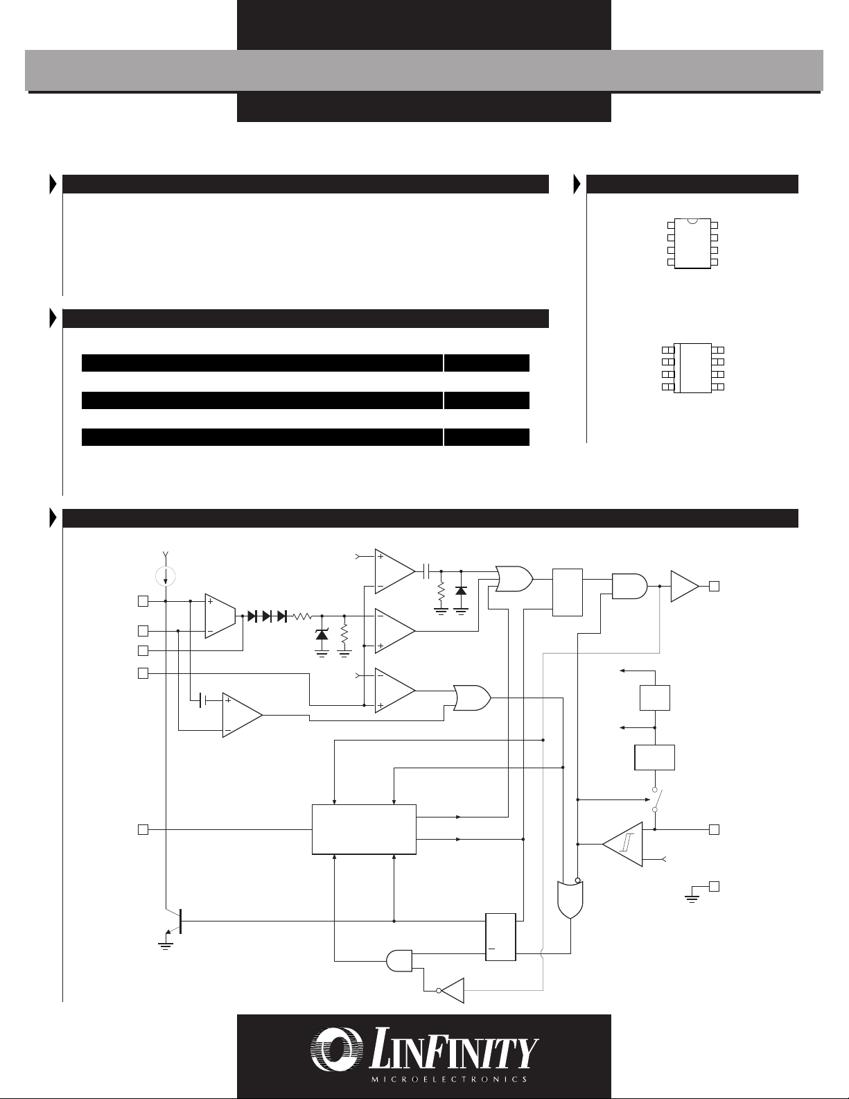
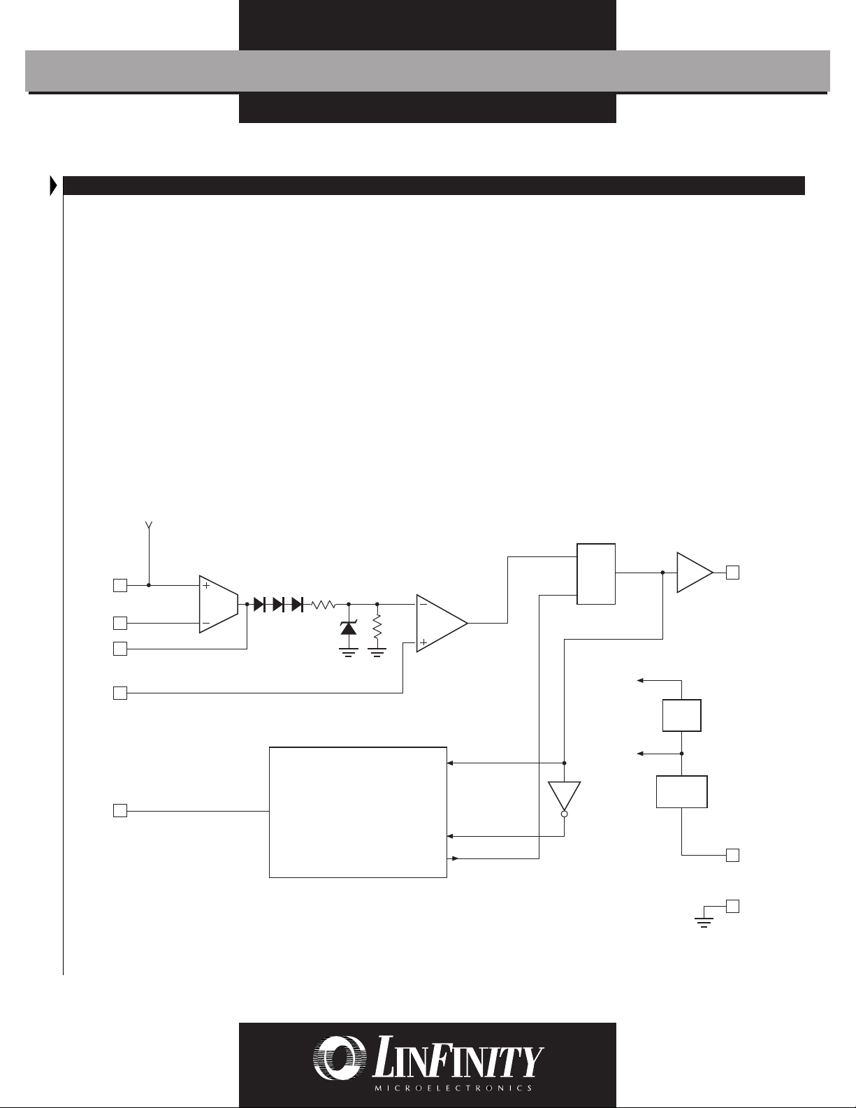
LX1571 BLOCK DIAGRAM
Minimum
Current Comp
C.S. Comp
Current Mode
Hiccup Comp
S.S.
V
OMP
C.S.
2.5V
0.5V
Error Amp
Voltage Hiccup
Comp.
1
2
FB
3
4
0.25V
2R
1V
R
1.5V
PWM Latch
RSQ
PACKAGE PIN OUTS
S.S.
1 8
V
27
FB
COMP
36
C.S.
45
M & Y PACKAGE
(Top View)
1 8
S.S.
27
V
FB
COMP
C.S.
2.5V
36
45
DM PACKAGE
(Top View)
2.5V
REF
C
V
OUT DRV
GND
6
OUT DRV
T
CC
C
T
V
CC
OUT DRV
GND
Voltage Mode Hiccup
QUICK
CHG
CONTROL
DISCH
CONTROL
Timing / Duty Cycle
8
C
T
CHG
CONTROL
Control
VALLEY
THRESHOLD
CONTROL
LATCH RESET
CONTROL
LATCH
SET CONTROL
Hiccup
Latch
RSQQ
2
5V
Internal
Bias
V
7
6V
16V
CC
5
GND
Copyright © 1997
Rev. 0.9.3 1/97
Page 3
PRODUCT DATABOOK 1996/1997
LX1570/1571
P
HASE MODULATED
P RELIMINARY DATA SHEET
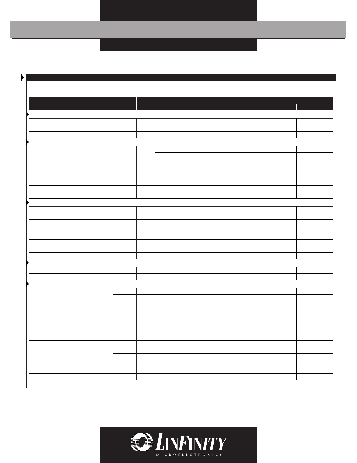
ELECTRICAL CHARACTERISTICS
(Unless otherwise specified, these specifications apply over the ranges TA = -55 to 125ºC for the LX1570M/1571M, TA = -40 to 85ºC for the
LX1570I/1571I, and T
Reference Section
Initial Accuracy VRITA = 25ºC, measured at F.B pin
Line Regulation ∆V
Temp Stability ∆V
Timing Section
Initial Accuracy f
Line Voltage Stability ∆f
Charging Current I
Discharging Current I
Leakage Current I
Ramp PK to PK V
Error Amp / Soft Start Comp Section
Transconductance g
Input Bias Current I
Open Loop Gain A
Output Sink Current I
Output Source Current I
Output HI Voltage V
Output LO Voltage V
Slew Rate S
Soft-Start Section
Soft Start Timing Factor K
Soft Start Discharge Current I
Current Sense Section
Input Range LX1570 V
Input Current LX1570 I
C.S. Amplifier Gain LX1570 A
Minimum Current Threshold Voltage LX1570 V
C.S. Delay to Driver Output 10% Overdrive
C.L. Pulse-By-Pulse Threshold Voltage LX1570 V
C.L. Hiccup Threshold Voltage LX1570 V
Voltage Hiccup Threshold V
Note 2. Although this parameter is guaranteed, it is not 100% tested in production.
= 0 to 70ºC for LX1570C/1571C. VCC = 15V. Typ. number represents TA = 25ºC value.)
A
Parameter
LX1571
LX1571
LX1571
LX1571
LX1571
LX1571
AC S
Symbol
RL
RT
O
OL
CHG
DISCH
LK
RPP
m
B
VOL
EA(SINK)VFB
EA(SOURCE)VFB
COMP-HI
COMP-LO
SS
SS-DIS
CSI
CSB
CS
CSMIN
CLP
CLH
HCCP
YNCHRONOUS SECONDARY-SIDE CONTROLLER
Test Conditions
11V < VCC < 25
Note 2
CT = , TJ = 25°C, measured at pin 6
Over Temp, measured at pin 6
C.S.
= 1.5V
INPUT
C.S.
= 0V
INPUT
C.S.
= 1.5V (1571), C.S.
INPUT
= 2.6V
= 2.4V
= -0.4V (1570)
INPUT
LX1570/1571
Min. Typ. Max.
2.475 2.500 2.525 V
±1 %
±1.5 %
90 100 110 kHz
85 100 115 kHz
±1 %
3mA
3.5 mA
4µA
0.6 V
6V
0.005 µΩ
0.1 1 µ A
60 70 dB
200 400 µA
200 400 µA
5.1 V
0.8 V
1 V/µSec
35 50 65 ms/µF
TBD mA
-0.8 V
-0.3 6 V
25 µA
1µA
-13.5 -15 -16.5 V/V
2.7 3 3.3 V/V
-50 mV
250 mV
100 200 ns
-0.18 -0.2 -0.22 V
0.9 1 1.1 V
-0.3 V
1.5 V
2V
Units
Copyright © 1997
Rev. 0.9.3 1/97
3
Page 4
PRODUCT DATABOOK 1996/1997
LX1570/1571
P
HASE MODULATED
P
ELECTRICAL CHARACTERISTICS (Con't.)
Parameter
PWM Section
E.A. Output to PWM Drive Offset V
Fixed Duty Cycle D
Output Drive Section
Rise / Fall Time tR / tFCL = 1000pF
Output HI V
Output LO V
Output Pull Down V
UVLO Section
Start-Up Threshold V
Turn Off Threshold V
Hysterises V
Supply Current Section
Dynamic Operating Current I
Start-Up Current I
AC S
RELIMINARY DAT A SHEET
Symbol
OFS
DHISOURCE
DLISINK
DPDVCC
ST
OFF
H
Qd
ST
YNCHRONOUS SECONDARY-SIDE CONTROLLER
Test Conditions Units
= 200mA, VCS = 0V, VFB = 2.3V
= 200mA, VCS = 1.2V, VFB = 2.3V
= 0V, I
Out Freq = 100kHz, CL = 0
PULL UP
= 2mA
LX1570/1571
Min. Typ. Max.
1.7 2.0 2.4 V
52 54 56 %
50 ns
13.5 V
0.8 V
1V
15 16 17 V
91011V
5.5 6 6.5 V
18 30 mA
150 250 µA
Pin # Description
S.S. 1
V
FB
COMP 3
C.S. 4
GND 5
OUT 6
DRV
V
CC
This pin acts as the soft-start pin. A capacitor connected from this pin to GND allows slow ramp up of the NI input
resulting in output soft start during start up. This pin is clamped to the internal voltage reference during the normal
operation and sets the reference for the feedback regulator.
This pin is the inverting input of the Error Amplifier. It is normally connected to the switching power supply output
2
through a resistor divider to program the power supply voltage. This pin instead of the NI pin is internally trimed to
1% tolerance to include the offset voltage error of the error amp.
This pin is the Error Amplifier output and is made available for loop compensation. Typically a series R&C network
is connected from this pin to GND.
A voltage proportional to the inductor current is sensed by an external sense resistor (1570) or current transformer (1571)
in series with the return line and is connected to this pin. The output drive is terminated and latched off when this voltage
amplified by the internal gain (see option table) exceeds the voltage set by the E.A output voltage. The maximum
allowable voltage at this pin during normal operation is -0.8V typ for LX1570 and 6V typ for LX1571.
This pin is combined control circuitry and power GND. All other pins must be positive with respect to this pin, except
for C.S pin.
This pin drives a gate drive transformer which drives the power mosfet. A Schottky diode such as 1N5817 must be
connected from this pin to GND in order to prevent the substrate diode conduction.
7
This pin is the positive supply voltage for the control IC. A high frequency capacitor must be closely placed and
connected from this pin to GND to provide the turn-on and turn-off peak currents required for fast switching of the power
Mosfet.
FUNCTIONAL PIN DESCRIPTIONFUNCTIONAL PIN DESCRIPTION
FUNCTIONAL PIN DESCRIPTION
FUNCTIONAL PIN DESCRIPTIONFUNCTIONAL PIN DESCRIPTION
C
4
8
T
The free running oscillator frequency is programmed by connecting a capacitor from this pin to GND.
Copyright © 1997
Rev. 0.9.3 1/97
Page 5

PRODUCT DATABOOK 1996/1997
P
HASE MODULATED
P RELIMINARY DATA SHEET
AC S
YNCHRONOUS SECONDARY-SIDE CONTROLLER
APPLICATION INFORMATION
LX1570/1571
20V-30V
100kHz - 150kHz
VIN (17 to 20V)
AC(+)
20-30V, 100-150kHz
Secondary Transformer
AC(-)
R6
324, 1%
R7
1k, 1%
C6
0.56µF
R10
5k
1%
R15
1M
C7
R2
300, 2W
D8
1N4937
IRLZ44
0.047µF
Q1
1N4148
R11
1.1k
C8
1000pF
D4
U1
LX1570
1
S.S.
V
COMP
C1
0.1µF, 50V
FB
T2
See Note 1
C2
0.1µF
R4
47
C
T
V
CC
OUT DRV
GNDC.S.
8
72
63
54
D1 1/2
MBR2545CT
R5
0.02, 5W
C5
1µF
L1
10µH (PE53700)
D1 2/2
MBR2545CT
See Note 2
C9
1500µF
C4
0.047µF
C10
1500µF
C11
1500µF
C12
1500µF
V
OUT (+)
3.3V / 7A
V
OUT (-)
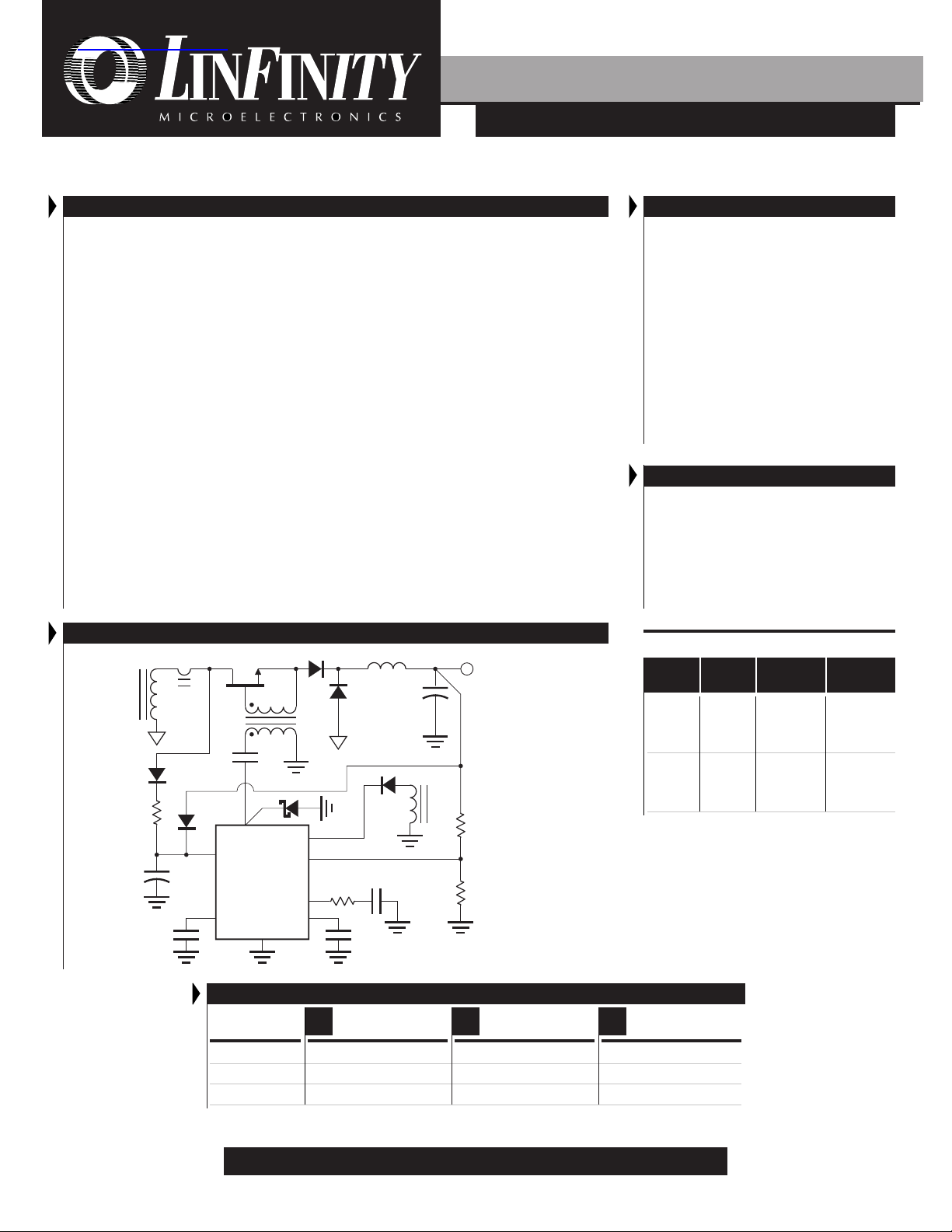
Note 1. T2 Core = RM4Z
2. For further information on PE53700 and PE64978,
contact Pulse Engineering at (619) 674-8100.
Copyright © 1997
Rev. 0.9.3 1/97
Np = 25T #28AWG
Ns = 25T #28AWG
FIGURE 1 — THE LX1570 IN A TYPICAL 3.3V / 7A SECONDARY-SIDE POWER SUPPLY APPLICATION
5
Page 6

LX1570/1571
PRODUCT DATABOOK 1996/1997
P
HASE MODULATED
P
AC S
YNCHRONOUS SECONDARY-SIDE CONTROLLER
RELIMINARY DAT A SHEET
APPLICATION INFORMATION
L1
(+)
Secondary
Transformer
Voltage
(-)
D2
R3
C3
C4
Q1
D3
T2
D4
8765
CTVCCOUT
U1, 1571
V
S.S.
FB
1234
C6
C2
R4
C5
GND
DRV
C.S.
COMP
R9 C10
1/2 D1
T1
R5
D6
D5
Pwr
Gnd
Signal Gnd
R10
1/2 D1
(Note A)
D7
C9
R6
V
V
OUT (+)
OUT (-)
R8
C7
FIGURE 2 — THE LX1571 IN A TYPICAL SECONDARY-SIDE POWER SUPPLY APPLICATION
6
C8
R7
Copyright © 1997
Rev. 0.9.3 1/97
Page 7
PRODUCT DATABOOK 1996/1997
V
P
HASE MODULATED
P RELIMINARY DATA SHEET
STEADY-STATE OPERATION
Steady-state operation is best described by referring to the main
block diagram and the typical application circuit shown in Figure 2. The output drive turns the external power MOSFET on
and current ramps up in the inductor. Inductor current is sensed
with an external resistor (or in the case of LX1571 with a current
transformer) and is compared to the threshold at the inverting
input of the current sense (C.S.) comparator. This threshold is
set by the voltage feedback loop, which is controlled by the
error amplifier. Exceeding this threshold resets the PWM latch
and turns the MOSFET off. The Output drive goes low, turning
charging current off and the discharging current on, caus-
the C
T
ing the C
1.5V, it sets the PWM latch and turns the output drive back on
prior to the next rising edge of the transformer voltage, and the
cycle repeats.
(Figure 4A) shows typical waveforms in the steady-state condi-
voltage to ramp down. When this voltage goes below
T
The Steady-State Operation Timing Diagram - Normal Mode
AC S
YNCHRONOUS SECONDARY-SIDE CONTROLLER
IC DESCRIPTION
LX1570/1571
tion. Notice that when the current sense signal turns the MOSFET
off, it also synchronizes the output drive to the transformer voltage (see discussion under heading Timing Section). In addition,
the energy transfer occurs only when both transformer voltage
and OUT DRV pin are "HI" at the same time, establishing the
effective on-time of the converter. This shows that the regulation of this converter is achieved by modulating the trailing edge
of the output drive with respect to the leading edge of the AC
voltage, while maintaining a fixed output drive duty cycle. In
other words, the converter duty cycle seen by L1 is controlled by
varying the phase between the AC voltage and the output driver
signal (phase modulation). Maximum converter duty cycle is
achieved when both signals are in phase, as shown in Figure 4B.
The LX1570/71 output drive always maintains a fixed duty cycle
(≈54%), since both charge and discharge currents are almost equal
as shown in Figures 4A and 4B.
S.S.
V
COMP
C.S.
2.5V
PWM Latch
R
1
2
FB
3
4
8
C
T
Error Amp
1V
Timing / Duty Cycle
Control
R
C.S. Comp
CHG
CONTROL
DISCH
CONTROL
LATCH
SET CONTROL
Q
S
2.5V
2.5V
REF
5V
Internal
Bias
OUT DR
6
V
7
CC
5
GND
Copyright © 1997
Rev. 0.9.3 1/97
FIGURE 3 — STEADY-STATE OPERATION BLOCK DIAGRAM
7
Page 8

LX1570/1571
PRODUCT DATABOOK 1996/1997
P
HASE MODULATED
P
AC S
YNCHRONOUS SECONDARY-SIDE CONTROLLER
RELIMINARY DAT A SHEET
IC DESCRIPTION
Transformer
Voltage
LX157x
OUT DRV
LX1571
C.S. Signal
Voltage
C
T
2µs / Div.
FIGURE 4A — STEADY-STATE OPERATION TIMING DIAGRAM
(NORMAL MODE)
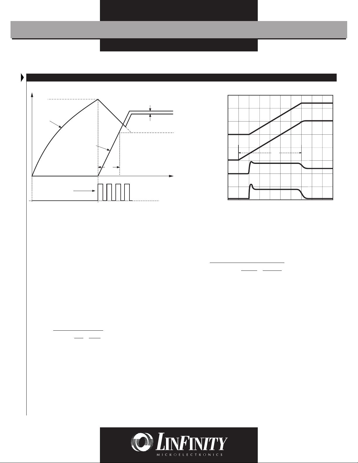
START-UP OPERATION
Using the main Block Diagram and the LX157x V
Voltage Timing Diagram (Figure 5) as a reference, when the V
Start-Up
CC
voltage passes the UVLO threshold (16V typ.), the output of the
UVLO comparator changes to the "HI" state, which causes the
following: a) provides biasing for internal circuitry, and b)
enables the output drive and the HICCUP latch. This signal sets
the "Q" output of the HICCUP latch "LO", allowing the soft-start
(S.S.) capacitor voltage to ramp up, forcing the regulator output
to follow this voltage. Since the IC provides a constant current
source for charging the S.S. capacitor, the resulting waveform is
a smooth linear ramp, which provides lower in-rush current
during start up.
The Start-Up Timing Diagram (Figure 6) shows the output
voltage and the S.S. capacitor during start up. Notice that the
output voltage does not respond to the S.S. capacitor until this
voltage goes above ≈0.65 volts, allowing this pin to be used as an
external shutdown pin. The value of the soft start capacitor must
be selected such that its ramp up time (t
the start up time of the converter, so that the converter is able to
) is always greater than
RAMP
follow the soft-start capacitor.
It is recommended that the soft start capacitor is always selected
such that its ramp up time (t
the converter's minimum start-up time. Equations 1 and 2 show
) be at least 4 times greater than
RAMP
how to select this capacitor.
CO * V
t
= 4
RAMP
Once t
calculated as follows:
*
is known, the soft-start capacitor can then be
RAMP
O
I
O
t
RAMP
= Equation 2
C
SS
35
Equation 1
Transformer
Voltage
LX157x
OUT DRV
LX1571
C.S. Signal
Voltage
C
T
2µs / Div.
FIGURE 4B — STEADY-STATE OPERATION TIMING DIAGRAM
(MAXIMUM DUTY CYCLE)
where C
CC
Example: If C
is in µF and t
SS
= 1600µF, VO = 12V, IO = 4A
O
1600 * 10-6 * 12
= 4 * = 19.2ms
t
RAMP
19.2
= = 0.55µF
C
SS
35
4
is in ms.
RAMP
The LX1570/71 series also features micropower start-up current
that allows these controllers to be powered off the transformer
voltage via a low-power resistor and a start-up capacitor. After the
IC starts operating, the output of the converter can be used to
power the IC. In applications where the output is less than the
minimum operating voltage of the IC, an extra winding on the
inductor can be used to perform the same function. The start-up
capacitor must also be selected so that it can supply the power to
the IC long enough for the output of the converter to ramp up
beyond the start-up threshold of the IC. Equation 3 shows how
to select the start-up capacitor.
t
I
*
Q
ST
C
where: I
Example: If I
C
= 2 Equation 3
ST
= 2 = 207µF
ST
V
H
≡ Dynamic operating current of the IC
Q
≡ Time for the bootstrap voltage to go above
t
ST
V
the minimum operating voltage (10V typ.)
≡ Minimum hysteresis voltage of the IC
HYST
= 30mA, tST = 19ms, V
Q
-3
30 * 10
* 19 * 10
5.5
-3
HYST
= 5.5V
8
Copyright © 1997
Rev. 0.9.3 1/97
Page 9
PRODUCT DATABOOK 1996/1997
V
V
P
HASE MODULATED
P RELIMINARY DATA SHEET
AC S
YNCHRONOUS SECONDARY-SIDE CONTROLLER
IC DESCRIPTION
LX1570/1571
16V
V
Cap
START UP
V
O
t
ST
OUT DRV
FIGURE 5 — LX157x VCC START-UP VOLTAGE TIMING DIAGRAM
V
O
V
CAP
10
Voltage - 5V / Div.
oltage - 1V / Div.
Output
Soft-Start
COMP Pin
L1 Current
t
RAMP
1ms / Div.
FIGURE 6 — START-UP TIMING DIAGRAM
TIMING SECTION
A capacitor connected from the C
eral functions. First, it sets the OUT DRV duty cycle to a constant
54% (regardless of the C
drive for an N-channel MOSFET, utilizing a simple gate drive
value) in order to: a) provide the gate
T
transformer, and b) insure reliable operation with a transformer
duty cycle within a 0 to 50% range. Second, it sets the free-
pin to ground performs sev-
T
Example: Assuming the transformer frequency is at 100kHz,
V
= 0.6V, I
RPP
C
T
CHG
=
.
∗∗∗
06 80 10
= 3mA, I
3
= 3.5mA.
DISCH
1
1
+
−−
33
∗
310135 10
.
∗
.µ
0033
F
=
running frequency of the converter in order to insure the continuous operation during non-steady state conditions, such as
start up, load transient and current limiting operations. The value
of the timing capacitor is selected so that the free-running frequency is always 20% below the minimum operating frequency
of the secondary transformer voltage, insuring proper operation.
Equation 4 shows how to select the timing capacitor CT.
C
=
T
Vf
where: V
RPP S
RPP
f
S
1
11
∗∗ +
II
CHG DISCH
≡ Peak to peak voltage of C
Equation 4
T
(0.6V typ.)
≡ Free-running frequency of the converter.
Selected to be 80% of the minimum freq.
of the seconday side transformer voltage.
I
≡ C
CHG
I
DISCH
charging current (3mA typ.)
T
≡ C
discharge current (3.5mA typ.)
T
CURRENT LIMITING
Using the main Block Diagram as a reference and the typical
application circuit of Figure 2, note that current limiting is performed by sensing the current in the return line using a current
transformer in series with the switch. The voltage at C.S. pin is
then amplified and compared with an internal threshold. Exceeding this threshold turns the output drive off and latches it off
until the set input of the PWM latch goes high again. However,
if the current keeps rising such that it exceeds the HICCUP comparator threshold, or if the output of the converter drops by
≈20% from its regulated point, two things will happen. First, the
HICCUP comparator pulls C
drive off and causes C
Second, it sets the HICCUP latch, causing the discharge current
to be turned off until the C
Since both charge and discharge currents are disconnected from
the capacitor, the only discharge path for C
current source. When this happens, a very slow discharge oc-
pin to 6V, which keeps the output
T
charging current to be disconnected.
T
capacitor voltage goes below 0.3V.
T
is the internal 2µA
T
curs, resulting in a long delay time between current limit cycles
which greatly reduces power MOSFET dissipation under short
circuit conditions.
Copyright © 1997
Rev. 0.9.3 1/97
9
Page 10

PRODUCT DATABOOK 1996/1997
LX1570/1571
P
HASE MODULATED
RELIMINARY DAT A SHEET
P
MINIMUM CURRENT COMPARATOR
One of the main advantages of replacing a Magnetic Amplifier
with a MOSFET, is the MOSFET's ability to respond quickly to
large changes in load requirements. Because the LX1570/71 relies on the C.S. signal for synchronization, special circuitry had to
be added to keep the output drive synchronized to the transformer voltage during such load transient conditions. This condition is best explained by referring to Figure 7. In Figure 7, it
can be seen that the load current is stepped from 0.4A to 4A,
causing the COMP pin to slew faster than the inductor current,
starting with the second switching cycle after the load transient
has occured. This condition eliminates the normal means of
resetting the PWM latch through the C.S. comparator path. To
compensate for this condition, a second comparator is ORed
with the C.S. comparator, which resets the latch on the falling
edge of the C.S. signal caused by the falling edge of the transformer voltage.
In other words, the function of the minimum C.S. comparator
is to turn OUT DRV off on the falling edge of the C.S. signal, if it
is not already off. This assures that the output drive is on before
the start of the next AC input cycle (Look-Ahead Switching™),
allowing maximum converter duty cycle.
AC S
YNCHRONOUS SECONDARY-SIDE CONTROLLER
IC DESCRIPTION
Transformer
Voltage
100V / Div.
LX157x
OUT DRV
20V / Div.
LX157x
COMP PIN
2V / Div.
Output Current &
Inductor Current
2A / Div.
FIGURE 7 — MINIMUM CURRENT COMPARATOR EFFECT
DURING LOAD TRANSIENT
ERROR AMPLIFIER
The function of the error amplifier is to set a threshold voltage
for inductor peak current and to control the converter duty cycle,
such that power supply output voltage is closely regulated.
Regulation is done by sensing the output voltage and comparing
it to the internal 2.5V reference. A compensation network based
on the application is placed from the output of the amplifier to
GND for closed loop stability purposes as well as providing high
DC gain for tight regulation. The function of "3V
keep output drive off without requiring the error amplifier output
" offset is to
BE
to swing to ground level. The transfer function between error
amp output (V
by:
- 3VBE = IP * G where:
V
COMP
) and peak inductor current is therefore given
COMP
I
= inductor peak current,
P
G = resistor divider gain,
(-15 for LX1570, 3 for LX1571)
V
= diode forward voltage
BE
(0.65V typ)
10
Copyright © 1997
Rev. 0.9.3 1/97
Page 11

PRODUCT DATABOOK 1996/1997
V
OUT (-)
V
OUT (+)
C10
820µF
16V
C9
820µF
16V
L1
140µH
1/2 D1
MUR1620
1/2 D1
MUR1620
T1
PE64978
R5
475
W
1%
1
43
2
C2
D4
1N4148
D3
1N4001
D2
1N4935
R4
(+)
(-)
Secondary
Transformer
Voltage
D8, 1N4937
R2, 2W
C1, 0.1µF
250V
Q1
IRF530
13
4
6
V
IN
C3
220µF
25V
CTVCCOUT
DRV
GND
C.S.
COMP
V
FB
S.S.
U1, LX1571
1234
8765
D6
1N5819
D5
1N5819
C5
1µF
C6
0.56µF
C7
R10
C13
C8
R11
D7
1N4148
R8
SHORT
R9
4.99
W
1%
R6
3.83k
W
1%
R7
1k
W
1%
C4
0.047µF
Signal Gnd
Pwr
Gnd
4.7k
N
S
N
P
0.1
(Note 1)
47
W
2.7k
1/2W
20k,1%
22pF
1000pF
4700pF
80V
f = 100 to 150kHz
T2
R3
100
W
12V/8A
R12
1M
W
Note 2
P
HASE MODULATED
P RELIMINARY DATA SHEET
AC S
YNCHRONOUS SECONDARY-SIDE CONTROLLER
12V/8A SCHEMATIC
Note: Linfinity provides a complete and
tested evaluation board. For further
information contact factory.
LX1570/1571
Copyright © 1997
Rev. 0.9.3 1/97
Core = RM4Z
N
T2
P
NS = 60T #32AWG
Unless otherwise noted all resistors are 1/4W, 5%.
Note 1: For further information on PE64978 contact Pulse Engineering at 619-674-8100.
Note 2: A high value resistor must be coupled back to "COMP" pin to insure proper operation under light load conditions.
= 20T #32AWG
FIGURE 8 — THE LX1571 IN A 12V/8A SECONDARY-SIDE POWER SUPPLY APPLICATION
11
Page 12

LX1570/1571
A
PRODUCT DATABOOK 1996/1997
P
HASE MODULATED
P
AC S
YNCHRONOUS SECONDARY-SIDE CONTROLLER
RELIMINARY DAT A SHEET
3.3V/10A SCHEMATIC
VP (10 to 30V)
V
P
f = 100kHz to 150kHz
(+)
Secondary
Transformer
Voltage
(-)
V
IN
(17 to 20V)
Core = RM4Z
= 25T #28AWG
N
T2
P
NS = 25T #28AWG
C3
22µF
25V
C4
0.047µF
300
D8, 1N4937
Q1
IRLZ44
1M
Note2
0.56µF
R2, 2W
W
13
6
1N4148
C6
C1, 0.1µF
50V
N
S
T2
4
N
P
D4
C2
0.1
R4
47
8765
CTVCCOUT
U1, LX1571
V
S.S.
1234
DRV
COMP
FB
5.49k, 1%
GND
C.S.
R10
C7
0.047µF
W
C5
1µF
C13
22pF
1/2 D1
MBR2545CT
43
1
PE64978
(Note 1)
Signal Gnd
W
100
R11
C8
1000pF
T1
R5
W
475
1%
D6
1N5819
D5
1N5819
Pwr
Gnd
2
R9
3.3
W
1%
L1
10µH
PE53700
(Note 1)
1/2 D1
MBR2545CT
R8
SHORT
D7
1N4148
Note: Linfinity provides a complete and
tested evaluation board. For further
information contact factory.
3.3V/10
C9
1500
µF
6.3V
1500
µF
6.3V
1500
µF
6.3V
1500
µF
6.3V
C12
C11
C10
R6
324
W
1%
R7
W
1k
1%
V
V
OUT (+)
OUT (-)
FIGURE 9 — THE LX1571 IN A 3.3V/10A SECONDARY-SIDE POWER SUPPLY APPLICATION
Unless otherwise noted all resistors are 1/4W, 5%.
Note 1: For further information on PE53700 and PE64978 contact Pulse Engineering at 619-674-8100.
Note 2: A high value resistor must be coupled back to "COMP" pin to insure proper operation under light load conditions.
Look-ahead SwitchingTM is a trademark of Linfinity Microelectronics Inc.
12
Copyright © 1997
Rev. 0.9.3 1/97
 Loading...