

Linear Technology RH1078M Datasheet

RH1078M
WU
U
PACKAGE
/
O
RDER I FOR ATIO
TOP VIEW
OUT BOUT A
V
+
–IN B–IN A
+IN B+IN A
V
–
8
7
6
5
3
2
1
4
H PACKAGE
8-LEAD TO-5 METAL CAN
Micropower, Dual, Single Supply
Precision Op Amp
DUESCRIPTIO
The RH1078M is a micropower dual op amp in the
standard 8-pin configuration. This device is optimized for
single supply operation at 5V. Specifications for ±15V are
also provided.
The wafer lots are processed to LTC’s in-house Class S
flow to yield circuits usable in stringent military applications.
U
U
BUR -I CIRCUIT
(Each Amplifier)
50k
20V
–
W
O
A
Supply Voltage ..................................................... ±22V
Differential Input Voltage ...................................... ±30V
Input Voltage ...............Equal to Positive Supply Voltage
...............................0.5V Below Negative Supply Voltage
Output Short-Circuit Duration ......................... Indefinite
Operating Temperature Range ............. – 55°C to 125°C
Storage Temperature Range ................ –55°C to 150°C
Lead Temperature (Soldering, 10 sec)................. 300°C
LUTEXI T
S
A
WUW
ARB
U
G
I
S
100Ω
+
50k
–20V
TOTAL DOSE BIAS CIRCUIT
10k
15V
–
10k
8V
Note: For ordering information contact LTC.
+
–15V
1
RH1078M
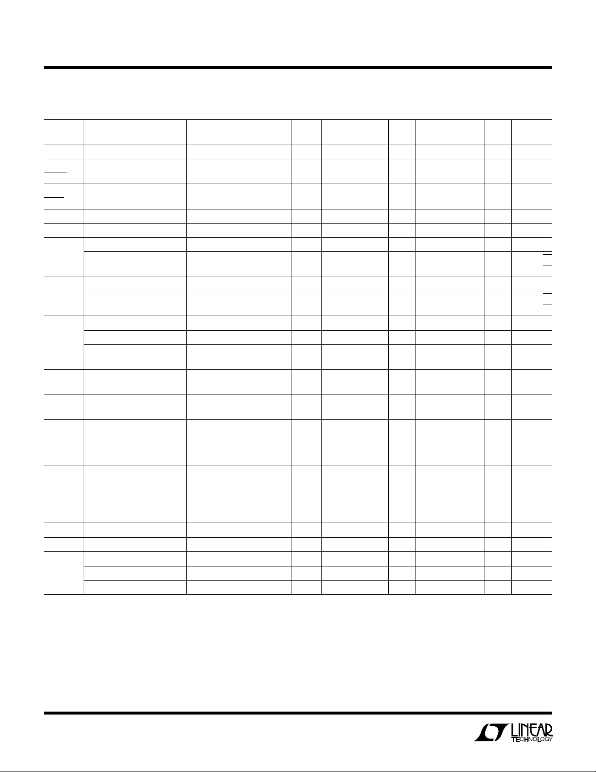
TABLE 1: ELECTRICAL CHARACTERISTICS
VS = 5V, VCM = 0.1V, V
SYMBOL PARAMETER CONDITIONS NOTES MIN TYP MAX GROUP MIN TYP MAX GROUP UNITS
V
OS
∆V
OS
∆Temp Offset Voltage
∆V
OS
∆Time
I
OS
I
B
e
n
i
n
R
IN
CMRR Common-Mode VCM = 0V to 3.5V 94 1 dB
PSRR Power Supply VS = 2.3V to 12V 100 1 dB
A
VOL
V
OUT
SR Slew Rate AV = 1, VS = ±2.5V 0.04 4 V/µs
GBW Gain-Bandwidth Product fO ≤ 20kHz 200 kHz
I
S
Input Offset Voltage 120 4 370 2, 3 µV
Average Tempco of 0.5 µV/°C
Long Term VOS Stability 0.5 µV/Month
Input Offset Current 0.8 1 1.5 2, 3 nA
Input Bias Current 15 1 18 2, 3 nA
Input Noise Voltage 0.1Hz to 10Hz 1 0.5 µVP-P
Input Noise Voltage Density fO = 10Hz 1 25 nV/√Hz
Input Noise Current 0.1Hz to 10Hz 1 2.6 pAP-P
Input Noise Current Density fO = 10Hz 1 0.07 pA/√Hz
Input Resistance Differential 2 600 MΩ
Common Mode 2 5 GΩ
Input Voltage Range 2 3.5 1 3.20 2, 3 V
Rejection Ratio VCM = 0.05V to 3.2V 88 2, 3 dB
Rejection Ratio V
Large-Signal Voltage Gain VO = 0.03V to 4V, No Load 150 1 V/mV
Output Voltage Swing Output Low, No Load 6 4 8 5, 6 mV
Supply Current per Amplifier 75 1 95 2, 3 µA
Channel Separation ∆VIN = 3V, RL = 10k 130 dB
Minimum Supply Voltage 3 2.3 V
= 1.4V unless otherwise specified.
OUT
= 1kHz 1 24 nV/√Hz
f
O
= 1kHz 1 0.025 pA/√Hz
f
O
= 3.1V to 12V 94 2, 3 dB
S
= 0.03V to 3.5V, RL = 50k 120 1 V/mV
V
O
= 0.05V to 4V, No Load 80 2, 3 V/mV
V
O
= 0.05V to 3.5V, RL = 50k 60 2, 3 V/mV
V
O
Output Low, 2k to GND 2 4 mV
Output Low, I
Output High, No Load 4.2 4 3.9 5, 6 V
Output High, 2k to GND 3.5 4 3.0 5, 6 V
= 100µA 130 4 170 5, 6 mV
SINK
2 0 1 0.05 2, 3 V
(Preirradiation)
TA = 25°C SUB- SUB-
–55°C ≤ TA ≤ 125°C
2
RH1078M
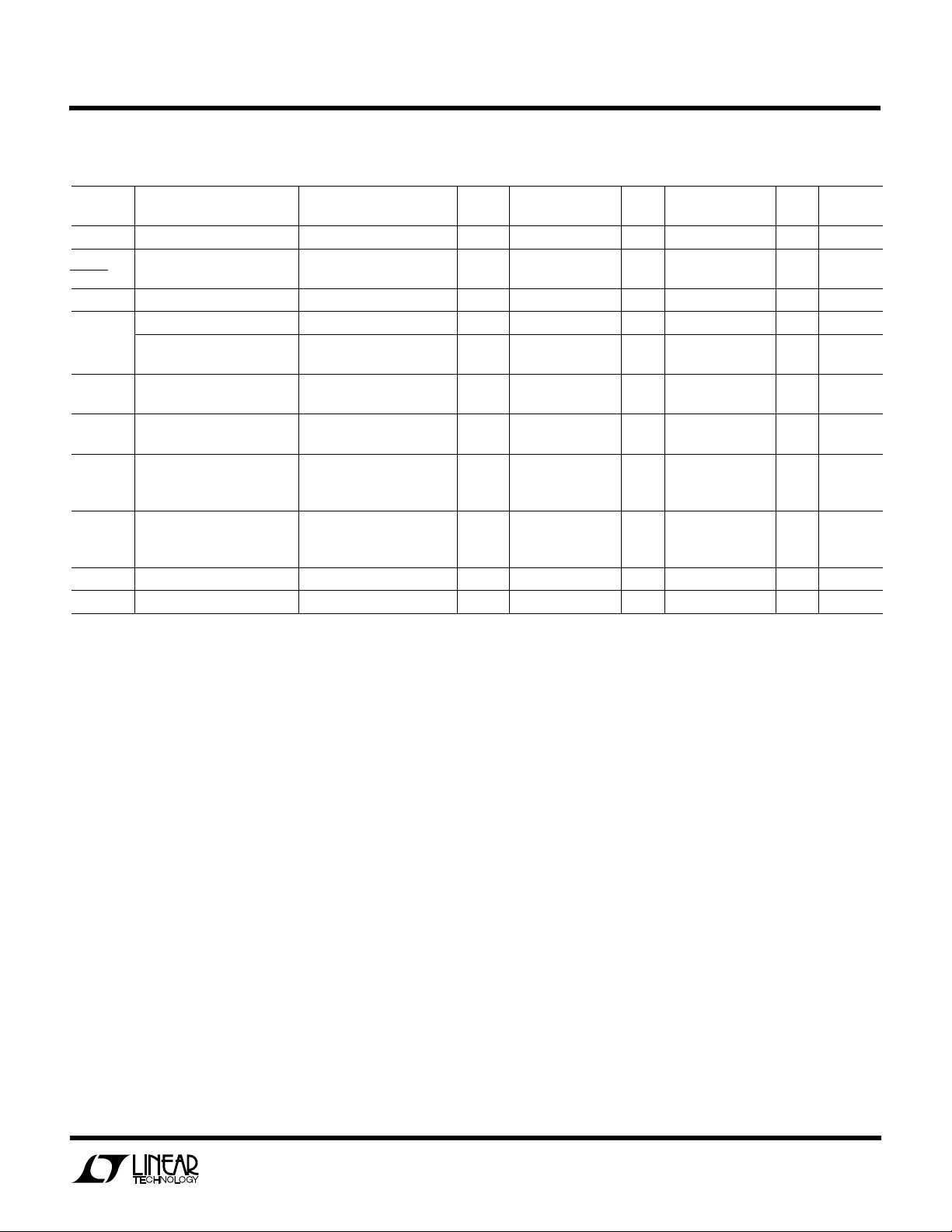
TABLE 1: ELECTRICAL CHARACTERISTICS
(Preirradiation)
VS = ±15V unless otherwise specified.
TA = 25°C SUB- SUB-
SYMBOL PARAMETER CONDITIONS NOTES MIN TYP MAX GROUP MIN TYP MAX GROUP UNITS
V
OS
∆V
OS
∆Temp Offset Voltage
I
OS
I
B
CMRR Common-Mode VCM = 13.5V, –15V 97 1 dB
PSRR Power Supply VS = 5V, 0V to ±18V 100 1 94 2, 3 dB
A
VOL
V
OUT
SR Slew Rate 0.06 4 V/µs
I
S
Input Offset Voltage 350 4 600 2, 3 µV
Average Tempco of 0.6 µV/°C
Input Offset Current 0.8 1 1.5 2, 3 nA
Input Bias Current 15 18 2, 3 nA
Input Voltage Range 13.5 1 V
–15.0 1 V
Rejection Ratio V
Rejection Ratio
Large-Signal Voltage Gain VO = ±10V, RL = 50k 1000 1 V/mV
Output Voltage Swing RL = 50k ±13 4 V
Supply Current Per Amplifier 100 1 125 2, 3 µA
= 13V, –14.9V 90 2, 3 dB
CM
= ±10V, RL = 2k 300 1 V/mV
V
O
VO = ±10V, RL = 5k 150 2, 3 V/mV
= 2k ±11 4 V
R
L
= 5k ±11 5, 6 V
R
L
–55°C ≤ TA ≤ 125°C
Note 1: All noise parameters are for VS = ±2.5V, VO = 0V.
Note 2: This parameter is guaranteed by design, characterization or
correlation to other tested parameters.
Note 3: Power supply rejection ratio is measured at the minimum supply
voltage. The op amps actually work at 1.8V supply but with a typical offset
skew of –300µV.
3
 Loading...