

Linear Technology RH1021-5 Datasheet
ABSOLUTE MAXIMUM RATINGS
W
WW
U
DESCRIPTION
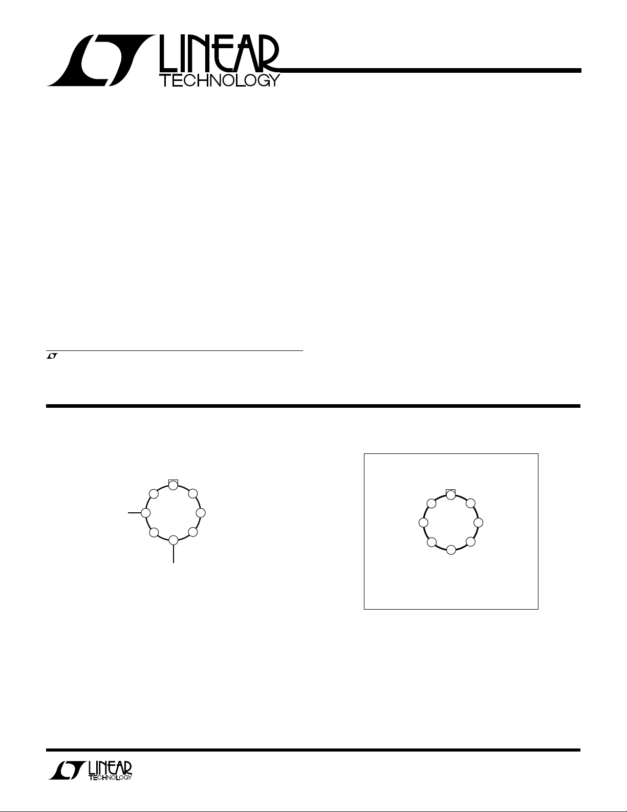
TOP VIEW
NC*
NC*
NC*
V
IN
V
OUT
TRIM
NC*
GND
8
7
6
5
2
1
4
H PACKAGE
8-LEAD TO-5 METAL CAN
3
RH1021-5
Precision 5V Reference
U
The RH1021-5 is a precision 5V reference with ultralow
drift and noise, extremely good long term stability and
almost total immunity to input voltage variations. The
reference output will source and sink up to 10mA. Unique
circuit design makes the RH1021-5 the first IC reference
to offer ultralow drift without the use of high power onchip heaters.
The wafer lots are processed to Linear Technology’s inhouse Class S flow to yield circuits usable in stringent
military applications.
, LTC and LT are registered trademarks of Linear Technology Corporation.
U U
BUR -I CIRCUIT
8
1
7
Input Voltage ........................................................... 40V
Input/Output Voltage Differential ............................. 35V
Trim Pin-to-Ground Voltage
Positive................................................ Equal to V
OUT
Negative ........................................................... –20V
Output Short-Circuit Duration
VIN = 35V........................................................ 10 sec
VIN 20V ................................................... Indefinite
Operating Temperature Range .............. –55°C to 125°C
Storage Temperature Range ................. –65°C to 150°C
Lead Temperature (Soldering, 10 sec).................. 300°C
U
W
U
PACKAGE/ORDER INFORMATION
220V
RH1021-5
3
–20V
6
5
4
* Connected internally. Do not connect external
circuitry to these pins.
1
RH1021-5
TABLE 1: ELECTRICAL CHARACTERISTICS
SYMBOL PARAMETER CONDITIONS NOTES MIN TYP MAX GROUP MIN TYP MAX GROUP UNITS
V
OUT
TCV
V
V
V
I
I
S
Output Voltage RH1021CM-5 1 4.9975 5.0025 1 V
RH1021BM-5, DM-5 1 4.95 5.05 1 V
Output Voltage RH1021BM-5 2 5 2,3 ppm/°C
OUT
Temperature Coefficient RH1021CM-5, DM-5 2 20 2,3 ppm/°C
Line Regulation 7.2V VIN 10V 3 12 1 20 2,3 ppm/V
OUT
IN
Load Regulation 0 I
OUT
(Sourcing Current)
OUT
Load Regulation 0 I
(Sinking Current)
Supply Current 1.2 1 1.5 2,3 mA
Output Voltage Noise 0.1Hz f 10Hz 4 3 µV
Long Term Stability T = 1000 Hrs 5 15 ppm
of V
OUT
Temperature Hysteresis T = ±25° Hrs 10 ppm
of V
OUT
10V VIN 40V 3 6 1 10 2,3 ppm/V
10mA 3 20 1 35 2,3 ppm/mA
OUT
10mA 3 100 1 150 2,3 ppm/mA
OUT
10Hz f 1kHz 4 3.5 4 µV
Noncumulative
(Preirradiation) (Note 8)
TA = 25°C SUB- SUB-
–55°C TA 125°C
P-P
RMS
TABLE 1A: ELECTRICAL CHARACTERISTICS
10Krad(Si) 20Krad(Si) 50Krad(Si) 100Krad(Si) 200Krad(Si)
SYMBOL PARAMETER CONDITIONS NOTES MIN MAX MIN MAX MIN MAX MIN MAX MIN MAX UNITS
V
OUT
TCV
V
V
V
I
I
S
Output Voltage RH1021CM-5 1 4.9975 5.0025 4.995 5.005 4.993 5.007 4.9925 5.008 4.99 5.01 V
RH1021BM-5, DM-5 1 4.95 5.05 4.945 5.055 4.942 5.058 4.94 5.06 4.935 5.065 V
Output Voltage RH1021BM-5 2 5 5 5 7 10 ppm/°C
OUT
Temperature Coefficient RH1021CM-5, DM-5 2 20 20 20 22 25 ppm/°C
Line Regulation 7.2V VIN 10V 3 12 12 13.5 15 18 ppm/V
OUT
IN
Load Regulation 0 I
OUT
(Sourcing Current)
OUT
Load Regulation 0 I
(Sinking Current)
Supply Current 1.2 1.2 1.2 1.2 1.2 mA
10V VIN 40V 3 6 6 6 7 9 ppm/V
10mA 3,7 20 20 20 20 20 ppm/mA
OUT
10mA 3 100 100 100 100 150 ppm/mA
OUT
(Postirradiation) (Note 6)
2
 Loading...