

Linear Technology RH1013M Datasheet
A
U
G
W
A
WUW
ARB
S
O
LUTEXI T
I
S
DUESCRIPTIO
RH1013M
Dual Precision
Operational Amplifier
The RH1013M is the first precision dual operational amplifier which directly upgrades designs in the industry standard 8-pin DIP LM158/MC1558/OP-221 pin configuration. Low offset voltage (300µV max), low drift ( 2.5µV/
°C), low offset current ( 1.5nA), and high gain (1.2 million
min) combine to make the RH1013M two truly precision
amplifers in one package.
The wafer lots are processed to Linear Technology’s inhouse Class S flow to yield circuits usable in stringent
military applications.
U U
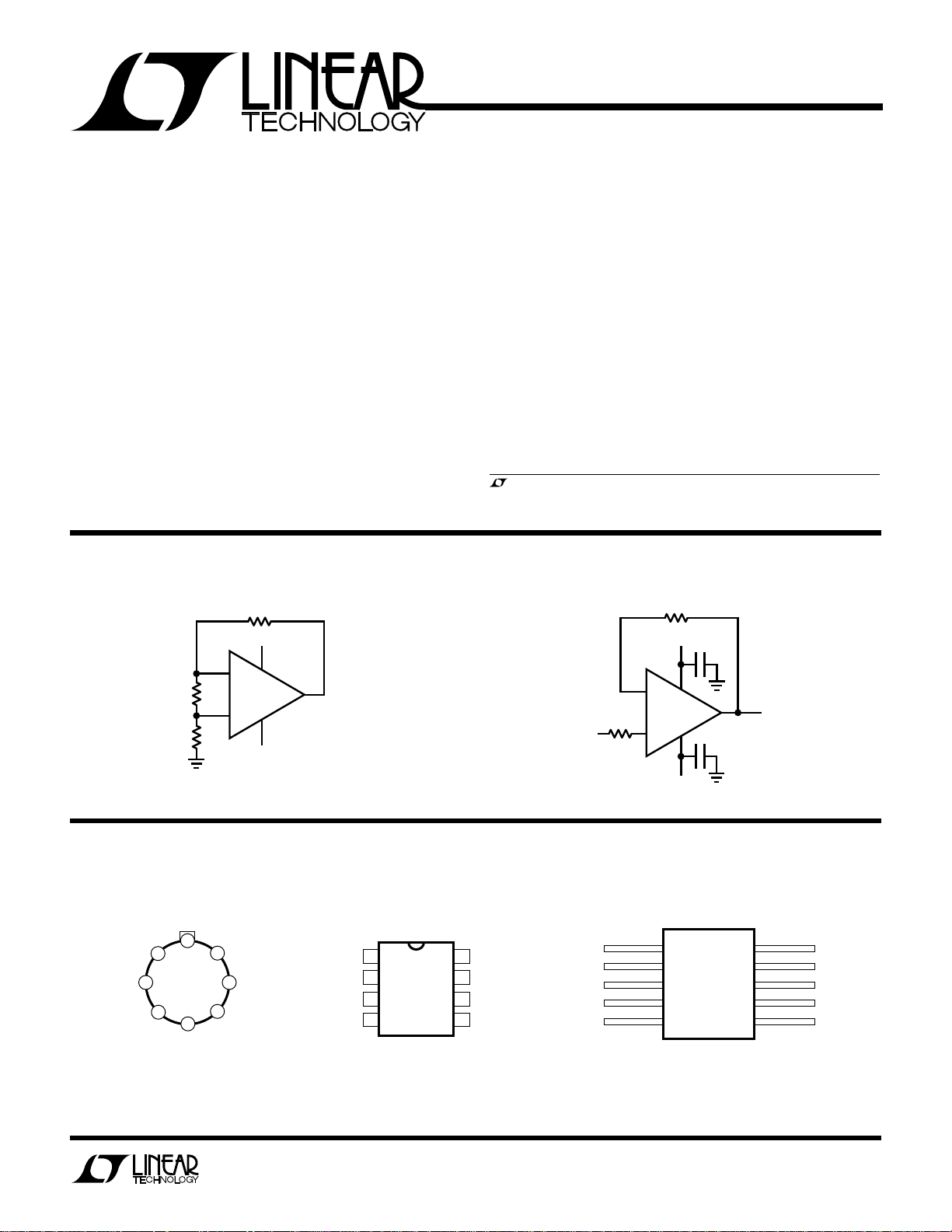
BUR -I CIRCUIT
50k
20V
100Ω
50k
RH1013M
–20V
RH1013M BI
Supply Voltage ..................................................... ±22V
Differential Input Voltage ...................................... ±30V
Input Voltage .............. Equal to Positive Supply Voltage
................................. 5V Below Negative Supply Voltage
Output Short-Circuit Duration ......................... Indefinite
Operating Temperature Range .............. – 55°C to 125°C
Storage Temperature Range ................. –65°C to 150°C
Lead Temperature (Soldering, 10 sec)..................300°C
, LTC and LT are registered trademarks of Linear Technology Corporation.
TOTAL DOSE BIAS CIRCUIT
10k
15V
–
10k
8V
+
–15V
RH1013M TDBC
/
TOP VIEW
V
8
1
3
4
–
(CASE)
V
H PACKAGE
O
RDER I FOR ATIO
+
OUT B
7
6
–IN B
5
+IN B
PACKAGE
OUT A
2
–IN A
+IN A
8-LEAD TO-5 METAL CAN
OUT A
–IN A
+IN A
–
V
WU
TOP VIEW
1
2
3
4
J8 PACKAGE
8-LEAD CERAMIC DIP
U
8
V+
7
OUT B
6
–IN B
5
+IN B
OUT A
–IN A
+IN A
NC
1
2
3
–
V
4
5
10-LEAD FLATPAK METAL SEALED
W PACKAGE
BOTTOM BRAZED
TOP VIEW
10
9
8
7
6
V+
OUT B
–IN B
+IN B
NC
1
RH1013M
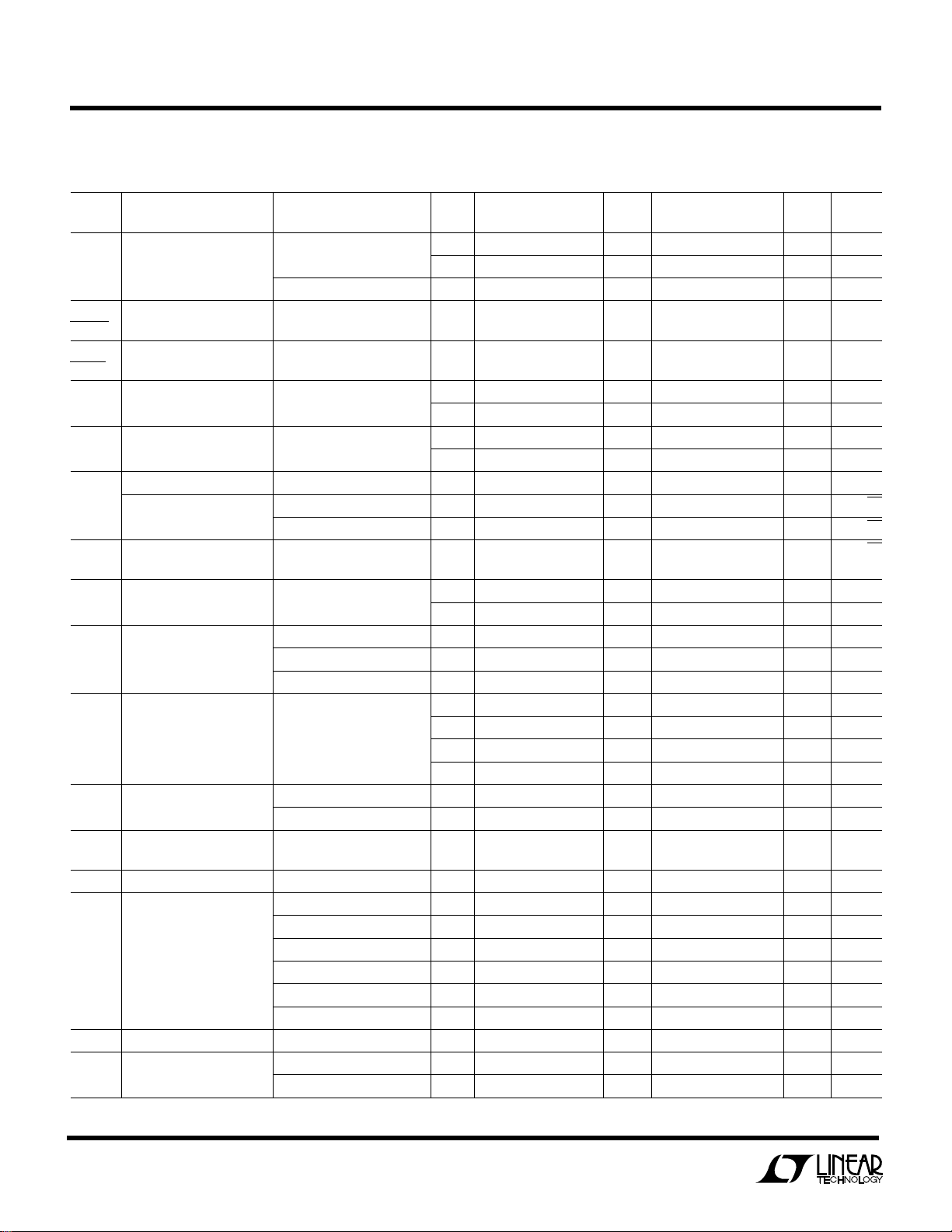
TABLE 1: ELECTRICAL CHARACTERISTICS
(Preirradiation)
VS = ±15V, VCM = 0V, unless otherwise noted.
TA = 25°C SUB- SUB-
SYMBOL PARAMETER CONDITIONS NOTES MIN TYP MAX GROUP MIN TYP MAX GROUP UNITS
V
OS
V
Temp Voltage
V
Time
I
OS
I
B
e
n
i
n
R
IN
A
VOL
CMRR Common-Mode Rejection VCM = 13.5V, –15V 97 1 dB
PSRR Power Supply Rejection VS = ±10V to ±18V 100 1 97 2,3 dB
V
OUT
SR Slew Rate 0.2 4 V/µs
I
S
Input Offset Voltage 300 1 550 2,3 µV
2 450 1 750 3 µV
VCM = 0.1V, TA = 125°C 750 2 µV
Average Tempco of Offset 1 2.5 µV/°C
OS
Long Term VOS Stability 0.5 µV/Mo
OS
Input Offset Current 10 1 20 2,3 nA
2 10 1 20 2,3 nA
Input Bias Current 30 1 45 2,3 nA
2 50 1 120 2,3 nA
Input Noise Voltage 0.1Hz to 10Hz 0.55 µV
Input Noise Voltage fO = 10Hz 24 nV/ Hz
Density fO = 1000Hz 22 nV/ Hz
Input Noise Current fO = 10Hz 0.07 pA/ Hz
Density
Input Resistance Differential 1 70 M
Common Mode 4 G
Large-Signal Voltage Gain VO = ±10V, RL 10k 1.2 4 0.25 5,6 V/µV
VO = ±10V, RL 600 0.5 4 V/µV
VO = 5mV to 4V, RL = 500 2 1 V/µV
Input Voltage Range 1 13.5 V
1 –15.0 V
1,2 3.5 V
1,2 0 V
Ratio VCM = 13V, –14.9V 94 2,3 dB
Ratio
Channel Separation VO = ±10V, RL = 2k 120 1 dB
Output Voltage Swing RL 2k ±12.5 4 ±11.5 5,6 V
Output Low, No Load 2 25 4 mV
Output Low, 600 to GND 2 10 4 18 5,6 mV
Output Low, I
Output High, No Load 2 4.0 4 V
Output High, 600 to GND 2 3.4 4 3.1 5,6 V
Supply Current Per Amplifier 0.55 1 0.70 2,3 mA
= 1mA 2 350 4 mV
SINK
2 0.50 1 0.65 2,3 mA
–55°C TA 125°C
P-P
2

TABLE 1A: ELECTRICAL CHARACTERISTICS (Postirradiation)
VS = ±15V, VCM = 0V, TA = 25°C, unless otherwise noted.
RH1013M
10KRAD(Si) 20KRAD(Si)
SYMBOL PARAMETER CONDITIONS NOTES MIN MAX MIN MAX MIN MAX MIN MAX MIN MAX UNITS
V
I
I
CMRR Common-Mode Rejection VCM = 13V, – 15V 97 97 94 90 86 dB
PSRR Power Supply Rejection VS = ±5V to ±18V 100 98 94 86 80 dB
A
V
SR Slew Rate RL 10k 0.13 0.12 0.11 0.07 0.01 V/µs
I
Input Ofset Voltage 450 450 600 750 900 µV
OS
2 600 600 750 900 µV
Input Offset Current 10 10 15 20 25 nA
OS
21010 15 20 nA
Input Bias Current 60 75 100 175 250 nA
B
2 80 100 125 200 nA
Input Voltage Range 1 13.5 13.5 13.5 13.5 13.5 V
1 –15.0 –15.0 –15.0 –15.0 –15.0 V
2 3.5 3.5 3.5 3.5 V
20 0 0 0 V
Ratio
Ratio
Large-Signal Voltage Gain RL 10k, VO = ±10V 500 200 100 50 25 V/mV
VOL
Maximum Output Voltage RL 10k ±12.5 ±12.5 ±12.5 ±12.5 ±12.5 V
OUT
Swing Output Low, No Load 2 25 30 40 50 mV
Output Low, 600 to GND 2 10 10 10 10 mV
Output Low, I
Output High, No Load 2 4.0 4.0 4.0 4.0 V
Output High, 600 to GND 2 3.4 3.2 3.0 2.8 V
Supply Current Per Amplifier 0.55 0.55 0.55 0.55 0.55 mA
S
= 1mA 2 0.6 0.8 1.0 1.6 V
SINK
2 0.50 0.50 0.50 0.50 mA
50KRAD(Si) 100KRAD(Si)
200KRAD(Si)
Note 1: Guaranteed by design, characterization, or correlation to other
tested parameters..
Note 2: Specification applies for V
= 1.4V.
V
OUT
U
W
TABLE 2: ELECTRICAL TEST REQUIRE E TS
MIL-STD-883 TEST REQUIREMENTS SUBGROUP
Final Electrical Test Requirements (Method 5004) 1*,2,3,4,5,6
Group A Test Requirements (Method 5005) 1,2,3,4,5,6
Group B and D for Class S, and 1,2,3
Group C and D for Class B
End Point Electrical Parameters (Method 5005)
* PDA applies to subgroup 1. See PDA Test Notes.
PDA Test Notes
The PDA is specified as 5% based on failures from group A, subgroup 1,
tests after cooldown as the final electrical test in accordance with method
5004 of MIL-STD-883. The verified failures of group A, subgroup 1, after
burn-in divided by the total number of devices submitted for burn-in in
that lot shall be used to determine the percent for the lot.
Linear Technology Corporation reserves the right to test to tighter limits
than those given.
+
= 5V, V
S
–
= 0V, VCM = 0V,
S
3
 Loading...