

Page 1
查询REF01AH供应商
FEATURES
■
Trimmed Output ±0.3%
■
Low Drift—5ppm/°C Typ
■
Low Noise—3ppm
■
High Line Rejection
■
Temperature Output—REF-02
■
Low Supply Current 1.4mA Max
(P-P)
U
APPLICATIO S
■
A/D and D/A Converters
■
Precision Regulators
■
Constant Current Sources
■
V/F Converters
■
Bridge Excitation
REF-01/REF-02
Precision
Voltage References
U
DESCRIPTIO
The REF-01/REF-02 are precision 10V and 5V bandgap
references which provide stable output voltages over a
wide range of operating conditions. Output voltage is
accurate to ±0.3% with a low 5ppm/°C typical temperature
coefficient. The REF-01 and REF-02 are excellent choices
for applications where low drift, moderate accuracy, low
power consumption and low cost are considerations.
The REF-02 includes a temperature output pin which
provides a linear voltage proportional to absolute temperature.
For lower drift and higher accuracy references, please see
the LT1019 and LT1021 data sheets.
, LTC and LT are registered trademarks of Linear Technology Corporation.
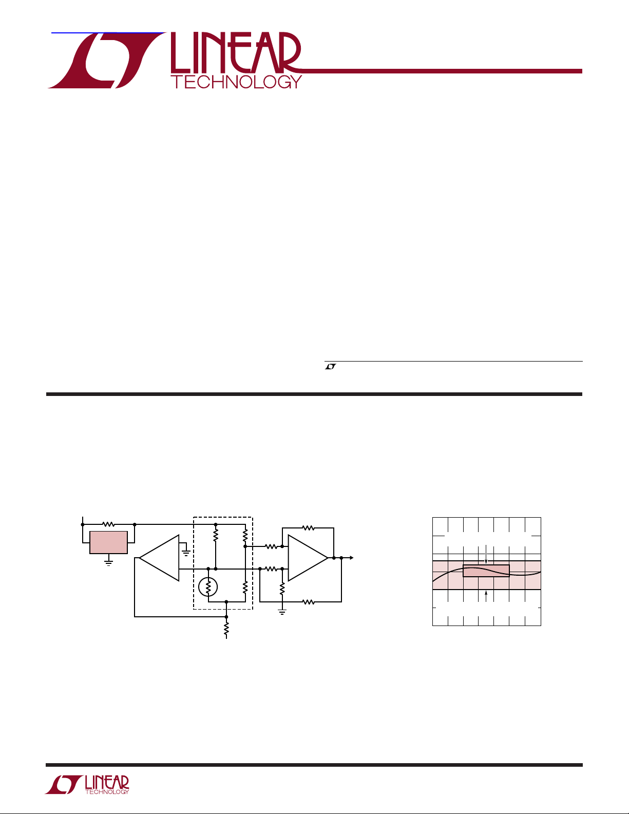
TYPICAL APPLICATIO
Ultra Linear Strain Gauge Amplifier
412Ω*
15V
1/2W
5V
REF-02
IN
OUT
GND
*
REDUCES REFERENCE AND AMPLIFIER LOADING.
**
IF R6 = R3, BRIDGE IS NOT LOADED BY R2 AND R4.
†
AND DRIFT ARE NOT CRITICAL.
A1 V
OS
A1
LT307
+
†
–
U
350Ω
BRIDGE
ACTIVE
ELEMENT
–5V
357Ω*
1/2W
–15V
20k
20k
Output Voltage Temperature Drift
R3
2M
R2
–
R4
2M
A2
LT1001
+
R5
R6
2M**
GAIN = 100
TA01a
1.003
0°C TO 70°C BOX GUARANTEED FOR
1.002
REF-01E AND REF-02E (8.5ppm/°C)
1.001
1.000
0.999
FULL TEMP RANGE BOX GUARANTEED FOR
0.998
OUTPUT VOLTAGE (NORMALIZED)
REF-01A AND REF-02A (8.5ppm/°C)
0.997
–50
–25 0
25 75
TEMPERATURE (°C)
50 100 125
TA01b
1
Page 2
REF-01/REF-02
WW
W
ABSOLUTE AXI U RATI GS
U
(Note 1)
REF-01/REF-02 A, E, H ............................................ 40V
REF-01C/REF-02C ................................................... 30V
Power Dissipation.............................................. 500mW
Output Short-Circuit Duration
To Ground ................................................... Indefinite
To VIN ≤ 16V ............................................... Indefinite
To VIN > 16V............................................Not Allowed
UUW
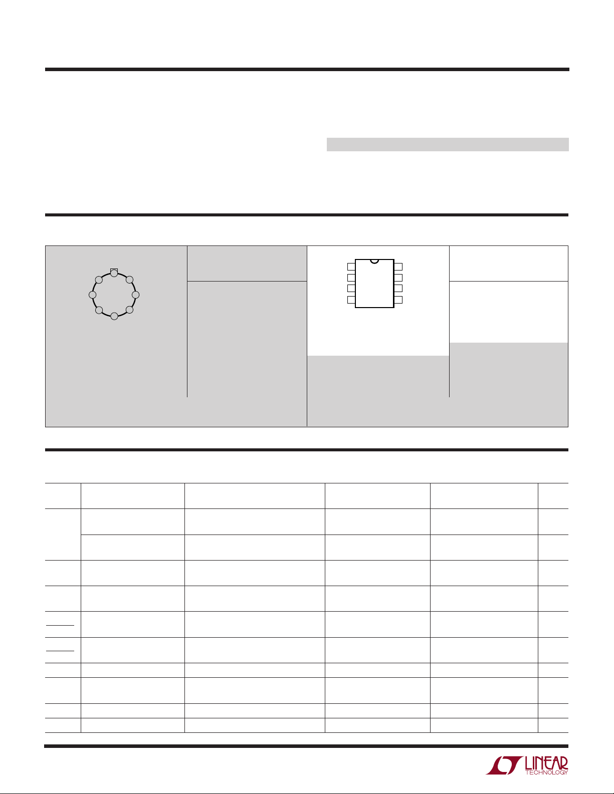
PACKAGE/ORDER I FOR ATIO
TOP VIEW
NC*
8
1
NC*
2
INPUT
3
TEMP**
GND (CASE)
H PACKAGE
8-LEAD TO-5 METAL CAN
= 150°C, θJA = 150°C/W, θJC = 45°C/W
T
JMAX
*INTERNALLY CONNECTED. DO
NOT CONNECT EXTERNALLY.
**DO NOT CONNECT ON REF-01
NC*
7
6
OUTPUT
5
TRIM
4
OBSOLETE PACKAGE
Consider the N Package for Alternate Source
Consult LTC Marketing for parts specified with wider operating temperature ranges.
ORDER PART
NUMBER
REF01AH
REF01H
REF01EH
REF01HH
REF01CH
REF02AH
REF02H
REF02EH
REF02HH
REF02CH
REF02DH
Storage Temperature Range ................. –65°C to 150°C
Operating Temperature
REF-01/REF-02, REF-01A/REF-02A ...–55°C to 125°C
REF-01E/REF-02E, REF-01H/REF-02H,
REF-01C/REF-02C, REF-01D/REF-02D .... 0°C to 70°C
Lead Temperature (Soldering, 10 sec).................. 300°C
TOP VIEW
NC*
1
INPUT
2
TEMP**
3
GND
4
N8 PACKAGE
8-LEAD PDIP
= 100°C, θJA = 130°C/W
T
JMAX
*INTERNALLY CONNECTED. DO
NOT CONNECT EXTERNALLY.
**DO NOT CONNECT ON REF-01
J8 PACKAGE
8-LEAD CERDIP
T
= 150°C, θJA = 100°C/W
JMAX
8
7
6
5
NC*
NC*
OUTPUT
TRIM
ORDER PART
NUMBER
REF01EN8
REF01HN8
REF01CN8
REF01EJ8
REF01HJ8
REF01CJ8
REF02EN8
REF02HN8
REF02CN8
REF02DN8
REF02EJ8
REF02HJ8
REF02CJ8
REF02DJ8
OBSOLETE PACKAGE
Consider the N Package for Alternate Source
ELECTRICAL CHARACTERISTICS
SYMBOL PARAMETER CONDITIONS MIN TYP MAX MIN TYP MAX UNITS
V
e
V
I
Q
I
OUT
I
SC
V
O
nP-P
IN
∆V
∆V
∆V
∆I
T
Output Voltage IL = 0mA REF-01 9.97 10 10.03 9.95 10 10.05 V
Output Adjustment Range RP = 10kΩ REF-01 ±3 5, –27 ±3 5, –27 %
Output Voltage Noise 0.1Hz to 10Hz (Note 7) REF-01 20 20 µV
Input Voltage Range REF-01 12 40 12 40 V
Line Regulation (V
OUT
(Note 2)
IN
Load Regulation IL = 0mA to 10mA REF-01 0.0005 0.008 0.0005 0.010 %/mA
OUT
(Note 2) REF-02 0.0010 0.010 0.001 0.010 %/mA
OUT
Quiescent Supply Current No Load 0.65 1.4 0.65 1.4 mA
Load Current 10 20 10 20 mA
Sink Current –0.3 –20 –0.3 –20 mA
Short-Circuit Current VO = 0V 25 25 mA
Temperature Voltage Output (Note 3) REF-02 Only 620 620 mV
+ 3V) ≤ VIN ≤ 33V 0.0001 0.010 0.0001 0.010 %/V
OUT
VIN = 15V, TA = 25°C unless otherwise noted.
REF-01A/E, REF-02A/E REF-01H, REF-02H
REF-02 4.985 5 5.015 4.975 5 5.025 V
REF-02 ±3 5, –13 ±3 5, –13 %
REF-02 10 10 µV
REF-02 7 40 7 40 V
P-P
P-P
2
Page 3
REF-01/REF-02
ELECTRICAL CHARACTERISTICS
SYMBOL PARAMETER CONDITIONS MIN TYP MAX MIN TYP MAX UNITS
V
e
I
Q
I
OUT
I
SC
V
O
nP-P
∆V
∆V
∆V
∆I
T
Output Voltage IL = 0mA REF-01 9.9 10 10.1 V
Output Adjustment Range RP = 10kΩ REF-01 5, –27 %
Output Voltage Noise 0.1Hz to 10Hz (Note 7) REF-01 30 µV
Line Regulation (V
OUT
(Note 2)
IN
Load Regulation IL = 0mA to 8mA 0.0005 0.015 %/mA
OUT
(Note 2) IL = 0mA to 4mA 0.001 0.04 %/mA
OUT
Quiescent Supply Current No Load 0.65 1.6 0.65 2 mA
Load Current 8 20 8 20 mA
Sink Current –0.2 20 –0.2 20 mA
Short-Circuit Current VO = 0V 25 25 mA
Temperature Voltage Output (Note 3) REF-02 Only 620 620 mV
+ 3V) ≤ VIN ≤ 33V 0.0001 0.015 0.0001 0.04 %/V
OUT
VIN = 15V, TA = 25°C unless otherwise noted.
REF-01C, REF-02C REF-02D
REF-02 4.95 5 5.05 4.9 5 5.1 V
REF-02 ±2.7 5, –13 ±2 5, –13 %
REF-02 12 12 µV
P-P
P-P
The ● denotes the specifications which apply over the full operating temperature range, otherwise specifications are at TA = 25°C.
VIN = 15V, –55°C ≤ TA ≤ ±125°C for REF-01A/REF-02A and REF-01/REF-02, 0°C ≤ TA ≤ 70°C for REF-01E/REF-02E and
REF-01H/REF-02H, IL = 0mA unless otherwise noted.
REF-01A/E, REF-02A/E REF-01H/REF-02H
SYMBOL PARAMETER CONDITIONS MIN TYP MAX MIN TYP MAX UNITS
∆V Output Voltage Change with 0°C␣ ≤ TA ≤ 70°C l 0.02 0.06 0.035 0.17 %
∆T Temperature (Notes 4, 5) –55°C ≤ T
TC Output Voltage Temperature (Note 6) l 5 8.5 8 25 ppm/°C
Coefficient
Change in VO Temperature RP = 10kΩ l 0.5 0.5 ppm/%
Coefficient with Output
Adjustment
∆V
∆V
∆V
∆I
Line Regulation 0°C ≤ TA ≤ 70°C l 0.0001 0.012 0.0001 0.012 %/V
OUT
(V
IN
OUT
OUT(IL
+ 3V) ≤ VIN ≤ 33V (Note 2) –55°C ≤ TA ≤ 125°C l 0.0001 0.015 0.0001 0.015 %/V
OUT
Load Regulation 0°C ≤ TA ≤ 70°C l 0.002 0.010 0.002 0.012 %/mA
= 0mA to 8mA) (Note 2) –55°C ≤ TA ≤ 125°C l 0.002 0.012 0.002 0.015 %/mA
Temperature Voltage Output (Note 3) REF-02 l 2.1 2.1 mV/°C
Temperature Coefficient
≤ 125°C l 0.09 0.15 0.144 0.45 %
A
3
Page 4

REF-01/REF-02
ELECTRICAL CHARACTERISTICS
The ● denotes the specifications which apply over the full operating
temperature range, otherwise specifications are at TA = 25°C. VIN = 15V, 0°C ≤ TA ≤ 70°C and IL = 0mA unless otherwise noted.
REF-01C, REF-02C REF-02D
SYMBOL PARAMETER CONDITIONS MIN TYP MAX MIN TYP MAX UNITS
∆V Output Voltage Change with (Notes 4, 5) l 0.45 1.7 %
∆T Temperature
TC Output Voltage Temperature (Note 6) l 8 65 8 250 ppm/°C
Coefficient
Change in VO Temperature RP = 10kΩ l 0.5 0.5 ppm/%
Coefficient with Output
Adjustment
∆V
∆V
∆V
∆I
Note 1: Absolute Maximum Ratings are those values beyond which the life
of a device may be impaired.
Note 2: Line and load regulation specifications include the effect of self
heating.
Note 3: Limit current in or out of Pin 3 to 50nA and capacitance on Pin 3
to 30pF.
Note 4: ∆V is defined as the absolute difference between the maximum
output voltage and the minimum output voltage over the specified
temperature range expressed as a percentage of nominal output.
Line Regulation VIN = 8V to 30V l 0.0001 0.018 0.0001 0.05 %/V
OUT
(Note 2)
IN
Load Regulation IL = 0mA to 5mA l 0.002 0.018 0.002 0.05 %/mA
OUT
(Note 2)
OUT
Temperature Voltage Output (Note 3) REF-02 l 2.1 2.1 mV/°C
Temperature Coefficient
Note 5: ∆V specification applies trimmed or untrimmed.
Note 6: TC is defined as ∆V divided by the temperature range, i.e.,
V
=
T
MAXTMIN
∆
–
does
100% test 10Hz to 1kHz noise.
∆V
V
MAXVMIN
=
V
OUT
TC
Note 7: 0.1Hz to 10Hz noise cannot be 100% tested on modern high
speed test equipment, so Linear Technology does not put a guaranteed
maximum specification on this parameter for standard units. 100% bench
testing of 0.1Hz to 10Hz noise is available on special request. To ensure
–
•100
low output noise, Linear Technology
Consult factory for details.
4
Page 5

PACKAGE DESCRIPTIO
SEATING
PLANE
0.010 – 0.045*
(0.254 – 1.143)
U
H Package
8-Lead TO-5 Metal Can (.230 Inch PCD)
(Reference LTC DWG # 05-08-1321)
0.335 – 0.370
(8.509 – 9.398)
DIA
0.305 – 0.335
0.040
(1.016)
MAX
(7.747 – 8.509)
0.016 – 0.021**
(0.406 – 0.533)
0.050
(1.270)
MAX
GAUGE
PLANE
0.165 – 0.185
(4.191 – 4.699)
0.500 – 0.750
(12.700 – 19.050)
REF-01/REF-02
REFERENCE
PLANE
0.027 – 0.045
45°TYP
0.028 – 0.034
(0.711 – 0.864)
0.110 – 0.160
(2.794 – 4.064)
INSULATING
STANDOFF
*
LEAD DIAMETER IS UNCONTROLLED BETWEEN THE REFERENCE PLANE
AND 0.045" BELOW THE REFERENCE PLANE
**
FOR SOLDER DIP LEAD FINISH, LEAD DIAMETER IS
(0.686 – 1.143)
PIN 1
(5.842)
0.016 – 0.024
(0.406 – 0.610)
OBSOLETE PACKAGE
0.230
TYP
H8 (TO-5) 0.230 PCD 1197
5
Page 6

REF-01/REF-02
PACKAGE DESCRIPTIO
U
J8 Package
8-Lead CERDIP (Narrow .300 Inch, Hermetic)
(Reference LTC DWG # 05-08-1110)
CORNER LEADS OPTION
(4 PLCS)
0.023 – 0.045
(0.584 – 1.143)
HALF LEAD
0.045 – 0.068
(1.143 – 1.727)
FULL LEAD
OPTION
0.300 BSC
(0.762 BSC)
0.008 – 0.018
(0.203 – 0.457)
NOTE: LEAD DIMENSIONS APPLY TO SOLDER DIP/PLATE
OR TIN PLATE LEADS
0° – 15°
OPTION
0.005
(0.127)
MIN
0.025
(0.635)
RAD TYP
0.045 – 0.065
(1.143 – 1.651)
0.014 – 0.026
(0.360 – 0.660)
0.405
(10.287)
MAX
87
12
65
3
4
0.220 – 0.310
(5.588 – 7.874)
0.015 – 0.060
(0.381 – 1.524)
0.100
(2.54)
BSC
0.200
(5.080)
MAX
0.125
3.175
MIN
J8 1298
6
OBSOLETE PACKAGE
Page 7

PACKAGE DESCRIPTIO
U
N8 Package
8-Lead PDIP (Narrow .300 Inch)
(Reference LTC DWG # 05-08-1510)
0.255 ± 0.015*
(6.477 ± 0.381)
0.400*
(10.160)
MAX
876
REF-01/REF-02
5
12
0.300 – 0.325
(7.620 – 8.255)
0.065
(1.651)
0.009 – 0.015
(0.229 – 0.381)
+0.035
0.325
–0.015
+0.889
8.255
()
–0.381
*THESE DIMENSIONS DO NOT INCLUDE MOLD FLASH OR PROTRUSIONS.
MOLD FLASH OR PROTRUSIONS SHALL NOT EXCEED 0.010 INCH (0.254mm)
TYP
0.045 – 0.065
(1.143 – 1.651)
0.100
(2.54)
BSC
3
4
0.130 ± 0.005
(3.302 ± 0.127)
0.125
(3.175)
MIN
0.018 ± 0.003
(0.457 ± 0.076)
0.020
(0.508)
MIN
N8 1098
Information furnished by Linear Technology Corporation is believed to be accurate and reliable.
However, no responsibility is assumed for its use. Linear Technology Corporation makes no representation that the interconnection of circuits as described herein will not infringe on existing patent rights.
7
Page 8

REF-01/REF-02
RELATED PARTS
PART NUMBER DESCRIPTION COMMENTS
LT1019 0.05%, 5ppm/°C Precision Reference Pin Compatible with the REF-01, REF-02, Improved Specs
8
Linear Technology Corporation
1630 McCarthy Blvd., Milpitas, CA 95035-7417
(408) 432-1900 ● FAX: (408) 434-0507
●
www.linear.com
ref012fc LT/CP 0901 1.5K REV C • PRINTED IN USA
LINEAR TECHNOLOGY CORPORATION 1991
 Loading...