

Page 1

LINEAR TECHNOLOGY
LINEAR TECHNOLOGY
LINEAR TECHNOLOGY
MARCH 2008 VOLUME XVIII NUMBER 1
IN THIS ISSUE…
COVER ARTICLE
Complete IF Receiver Has
16-Bit, 130Msps ADC, Fixed-Gain
Amplifier and Antialias Filter in
11.25mm × 11.25mm
µModule™ Package .............................1
Todd Nelson
Linear in the News… ...........................2
DESIGN FEATURES
Voltage and Current Monitoring from
7V to 80V in 3mm × 3mm DFN-10 ........5
Zhizhong Hou
Increase I2C or SMBus Data Rate and
Reduce Power Consumption with
Low Power Bus Accelerator .................8
Sam Tran
6-Input Supervisors Offer Accurate
Monitoring and 125°C Operation ......10
Shuley Nakamura and Al Hinckley
High Power, Single Inductor,
Surface Mount Buck-Boost µModule
Regulators Handle 36VIN, 10A Loads
.........................................................16
Manjing Xie
1.5% Accurate Single-Supply
Supervisors Simplify Part Selection
and Operate to 125°C ........................20
Bob Jurgilewicz and Roger Zemke
Versatile Current Sense Amplifiers
Offer Rail-to-Rail Input, 150°C
Operating Temperature ....................24
William Jett and Glen Brisebois
Compact Hot Swap™ Solution
Simplifies Advanced Mezzanine
Card Design ......................................27
Chew Lye Huat
DESIGN IDEAS
....................................................
(complete list on page 31)
New Device Cameos ...........................37
Design Tools ......................................39
Sales Offices .....................................
31–36
40
Complete IF Receiver
Has 16-Bit, 130Msps ADC,
Fixed-Gain Amplifier
and Antialias Filter in
11.25mm × 11.25mm
µModule Package
by Todd Nelson
Introduction
In the design of high speed receivers for communications, test or
instrumentation equipment, several
specialized disciplines converge in
one place—the analog-to-digital converter (ADC). Unfortunately, the ADC
is not a simple black box where an
RF designer applies the signal and a
digital designer retrieves the accurate
output. Careful design of the signal
conditioning circuitry to drive the ADC
is critical. Something as seemingly
straightforward as board layout can
degrade the downstream signal by a
few precious decibels. The problem
is that the disciplines required for
the engineering on either side of the
ADC, namely RF/IF design and digital
design, do not include mastery of the
art of ADC interface design. Someone
has to put in the effort to properly drive
the ADC. But who? Instead of adding
more work to either designer’s plate,
what if the ADC were really a black
box, already loaded with integrated
signal conditioning components in an
optimized layout? Now, that would be
a better solution.
The LTM9001 is built using
Linear Technology’s µModule
technology to create an IC
form factor System-in-a-
Package (SiP) that includes
a high speed 16-bit ADC,
antialiasing filter and a low
noise, differential amplifier
with fixed gain. It can
digitize wide dynamic range
signals with an intermediate
frequency (IF) range
up to 300MHz.
The LTM9001 is exactly that black
box. It is built using Linear Technology’s µModule™ technology to create
an IC form factor System-in-a-Package
(SiP) that includes a high speed 16bit ADC, antialiasing filter and a low
noise, differential amplifier with fixed
gain. It can digitize wide dynamic range
continued on page 3
L
, LT, LTC, LTM, Burst Mode, OPTI-LOOP, Over-The-Top and PolyPhase are registered trademarks of Linear Technology
Corporation. Adaptive Power, Bat-Track, BodeCAD, C-Load, DirectSense, Easy Drive, FilterCAD, Hot Swap, LinearView,
µModule, Micropower SwitcherCAD, Multimode Dimming, No Latency ΔΣ, No Latency Delta-Sigma, No R
Filter, PanelProtect, PowerPath, PowerSOT, SmartStart, SoftSpan, Stage Shedding, SwitcherCAD, ThinSOT, True Color PWM,
UltraFast and VLDO are trademarks of Linear Technology Corporation. Other product names may be trademarks of the
companies that manufacture the products.
, Operational
SENSE
Page 2
CLKOUT
OF
LO
V
CC
= 3.3V V
DD
= 3.3V
ENC+ENC
–
ADC CONTROL PINS
DIFFERENTIAL
FIXED GAIN
AMPLIFIER
16-BIT
130Msps ADC
RF
IN
–
IN
+
LTM9001
SENSE
GND
D15
•
•
•
D0
0VDD = 0.5V TO 3.6V
OGND
CMOS
OR
LVDS
SAW
ANTI-ALIAS
FILTER
LTM9001, continued from page 1
DESIGN FEATURES L
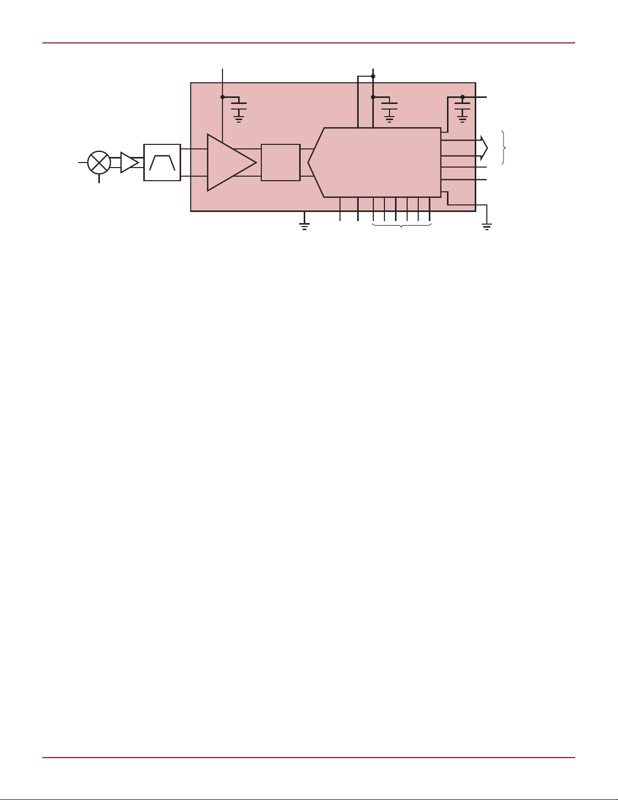
Figure 1. A typical application and simplified block diagram of the LTM9001
signals with an intermediate frequency
(IF) range up to 300MHz. Figure 1
shows a typical application.
How is a µModule component
different than a traditional IC? The
µModule construction allows the
LTM9001 to mix standard ADC and
amplifier components regardless of
their process technology and match
them with passive components for
a particular application. The result
is a high performance product with
no process technology compromises
and the potential for semi-custom
adaptations.
What’s Inside?
The µModule receiver consists of wirebonded die, packaged components and
passives mounted on a high performance, 4-layer, Bismaleimide-Triazine
(BT) substrate. BT is similar to other
laminate substrates such as FR4 but
has superior stiffness and a lower
coefficient of thermal expansion.
In time, several different versions
of the LTM9001 will be available. The
LTM9001-AA, as the first release, is
configured with a 16-bit, 130Msps
ADC. The amplifier gain is 20dB with
an input impedance of 200Ω and an
input range of ±250mV. The matching network is designed to optimize
the interface between the amplifier
outputs and the ADC inputs under
these conditions. Additionally, there
is a second order bandpass filter
designed for 162.5MHz, ±25MHz to
prevent aliasing and to limit the noise
from the amplifier.
Linear Technology Magazine • March 2008
Extracting the full performance
from 16-bit, high speed ADCs requires
careful layout as well as good circuit
design. The substrate design carefully
shields sensitive analog traces, maximizes thermal conduction through
multiple ground pads and minimizes
coupled noise by including bypass
capacitors inside the module and close
to the ADC. A common problem with
traditional ADC board layouts is long
traces from the bypass capacitors to
the ADC. The bare die construction
with internal bypass capacitors provides the closest possible decoupling
and eliminates the need for external
bypass capacitors.
The passive filter network implements an antialias filter and matches
the amplifier outputs to the ADC inputs. Most communications receiver
applications utilize a highly selective
filter between the mixer and the ADC
driver. The antialias filter between
the ADC driver and the ADC inputs
limits the wideband amplifier noise
and helps preserve the high SNR of
the ADC. Printed circuit board (PCB)
layout has a significant impact on the
performance even if the circuit topology and component values are correct.
The signal paths must be symmetric
and isolated from the clock inputs and
digital outputs.
The low noise, low distortion amplifier stage provides gain without adding
significant noise or distortion to the
signal. Despite the low noise of the
amplifier, the noise is multiplied by the
same gain as the amplifier, so higher
gain unavoidably adds noise to the
system. However, the input range of
the amplifier is proportionately smaller
thanks to the gain and this smaller
input range allows for lower distortion
from the preceding components. The
amplifier inputs present a resistive
200Ω differential input impedance
which is simple to match to most
common, high speed, single-ended or
differential signal paths. This presents
a more straightforward interface than
a switched-capacitor ADC and simplifies the connection to the final stage
of the RF signal chain.
Why 162.5MHz?
The ADC inside the LTM9001 has
a full power bandwidth of 700MHz
and the amplifier is suitable for input frequencies up to 300MHz, so
why was 162.5MHz chosen for this
first version? Nyquist theory tells us
that the minimum sample rate for a
given input frequency is twice that
frequency. Working backwards, an
ADC sampling at 130Msps can capture a frequency range up to 65MHz
wide. Undersampling allows us to
move that frequency range. Hence
the first Nyquist zone is DC – 65MHz,
the second is 65MHz to 130MHz, the
third is 130MHz to 195MHz, and so
on, see Figure 2.
instrumentation applications. In such
applications, the linearity and dynamic
range requirements are extremely
high. Traditional instruments utilize
preselectors and multiple down-con-
The LTM9001-AA is intended for
3
Page 3

L DESIGN FEATURES
FFT BIN NUMBER (32k TOTAL)
0
AMPLITUDE (dBFS)
–80
–60
–40
–20
0
12288
–100
–120
4096
20480 28672
HD2HD3
NYQUIST ZONE 1
DC TO 65MHz
DC CENTER = 32.5MHz 65MHz
NYQUIST ZONE 2
65MHz TO 130MHz
CENTER = 97.5MHz f
SAMPLE
NYQUIST ZONE 3
130MHz TO 195MHz
CENTER = 162.5MHz 195MHz
NYQUIST ZONE 4
195MHz TO 260MHz
CENTER = 227.5MHz 260MHz
Figure 2. Nyquist zones for 130MHz sample rate
version stages to place the band of
interest at DC. With the advent of high
performance ADCs capable of undersampling, modern instruments are able
to eliminate the final down-conversion
stage without sacrificing performance.
The LTM9001-AA configuration selects the third Nyquist zone with the
bandpass filter set squarely in the
middle of the zone.
More than Just
a Buffered ADC
The sample-and-hold front end of
discrete ADCs presents a complex
charge/discharge profile to the drive
circuitry. Ideally, the input circuitry
should be fast enough to fully charge
the sampling capacitor during the
sampling period (half of the clock
period), but this is not always possible and the incomplete settling may
degrade the SNR and SFDR. Some
manufacturers promote a “buffered”
ADC as a solution but this falls short
of addressing the system-level solution
since a low distortion amplifier is still
required to provide the full-scale input
to the ADC.
From the system view, the ADC
follows the RF and IF portions of the
receiver chain and converts the signal
to a digital format. The signal comes
from the antenna with very little power.
Figure 3. An FFT of the LTM9001 at 160MHz
input frequency with the randomizer on
4
The signal must be filtered and amplified through each stage. Amplification
(gain) increases the total noise and
reduces the headroom, which generally causes more distortion. The added
distortion may be addressed with a
higher supply voltage or a higher power
amplifier, neither of which is preferable. Therefore, from the system-level
point of view, an ADC with a small
input range is better.
The LTM9001 meets these systemlevel criteria. The resistive amplifier
inputs are easily matched and it has
an input range of ±250mV, enabling
the use of low OIP3 components or
higher loss SAW filters. The noise of
the amplifier is low enough that the
SNR of the LTM9001 is good despite
the high gain (see Figure 3).
Working with a
µModule Receiver
The LTM9001 uses a land grid array
(LGA), which provides higher pin density than dual in-line or quad packages
and better thermal conduction than
BGA packages. The high integration
of the LTM9001 makes the PCB board
layout simple. The multilayer substrate
allows greater flexibility in pin placement on the package relative to pin
placement on the die. The LTM9001
has been optimized for a flow-through
layout so that the interaction between
inputs, clock and digital outputs is
minimized. The analog and clock inputs are surrounded by ground pads
and a continuous row of ground pads
further separate the analog and digital
signal lines. However, to optimize its
electrical and thermal performance,
some layout considerations are still
necessary. See the actual evaluation
board in Figure 4.
Use large PCB copper areas for
ground. This helps to dissipate heat
through the board and also helps
to shield sensitive on-board analog
signals. Common ground (GND) and
output ground (OGND) are electrically
isolated on the LTM9001, but for most
digital output configurations should
be connected on the PCB underneath
the part to provide a common return
path.
Use multiple ground vias. Using as
many vias as possible helps to improve
the thermal performance of the board
and creates necessary barriers separating analog and digital traces on the
board at high frequencies. Take care to
separate analog and digital traces as
much as possible, using vias to create
high frequency barriers. This reduces
digital feedback that can reduce the
signal-to-noise ratio (SNR) and dynamic range of the LTM9001.
Conclusion
µModule technology, introduced first
by Linear Technology for DC/DC converters, now brings the advantages of
small size, higher integration and ease
of use for high speed ADC applications.
By integrating fine-line CMOS and
SiGe components with appropriate
passive networks, the challenging
task of matching a fixed gain amplifier to a high speed ADC is done. All is
reduced to an easy-to-use black box:
the LTM9001.
Figure 4. An evaluation board shows the
small overall circuit. Note that no external
components are required.
Linear Technology Magazine • March 2008
L
 Loading...