


DESIGN IDEAS L
GND
LTM8040
V
IN
SHDN
V
IN
14V TO 36V
C1
2.2µF
LEDA
LPWR
ADJ
PWM
RT
BIAS
1A
LED
CURRENT
500mA/DIV
ADJ PIN
VOLTAGE
500mV/DIV
5ms/DIV
0 AMPS
0 VOLTS
GND
LTM8040
V
IN
SHDN
V
IN
4V TO 36V
C1
2.2µF
5.11k
LEDA
LPWR
ADJ
PWM
BIAS
GND
LTM8040
V
IN
SHDN
V
IN
4V TO 36V
C1
2.2µF
LEDA
LPWR
ADJ
PWM
BIAS
1A
LED
CURRENT
500mA/DIV
PWM
SIGNAL
5V/DIV
20ms/DIV
DN445 F05
µModule LED Driver Integrates All
Circuitry, Including the Inductor,
in a Surface Mount Package
Introduction
Once relegated to the hinterlands of
low cost indicator lights, the LED is
again in the spotlight of the lighting
world. LED lighting is now ubiquitous,
from car headlights to USB-powered
lava lamps. Car headlights exemplify
applications that capitalize on the
LED’s clear advantages—unwavering
high quality light output, toughas-steel robustness, inherent high
efficiency—while a USB lava lamp
exemplifies applications where only
LEDs work. Despite these clear advantages, their requirement for regulated
voltage and current make LED driver
circuits more complex than the vener-
able light bulb, but some new devices
are closing the gap. For instance,
the LTM®8040 µModule LED driver
integrates all the driver circuitry into
a single package, allowing designers
Figure 1. Driving an LED string with the
LTM8040 is simple—just add the input
capacitor and connect the LED string
to refocus their time and effort on the
details of lighting design critical to a
product’s success.
A Superior LED Driver
The LTM8040 is a complete step-down
DC/DC switching converter system
that can drive up to 1A through a
string of LEDs. Its 4V to 36V input
voltage range makes it suitable for a
wide range of power sources, including 2-cell lithium-ion battery packs,
rectified 12VAC and industrial 24V.
The LTM8040 features both analog and
PWM dimming, allowing a 250:1 dimming range. The built-in 14V output
voltage clamp prevents damage in the
case of an accidental open LED string.
The default switching frequency of the
LTM8040 is 500kHz, but switching
frequencies to 2MHz can be set with a
resistor from the RT pin to GND.
by David Ng
Figure 2. Drive a 0V to 1.25V voltage into the ADJ pin to control the LED current amplitude
Figure 3. Control the LED current with
a single resistor from ADJ to ground
Linear Technology Magazine • September 2009
Figure 5. The LTM8040 can PWM LED current with minimal
distortion, even at frequencies as low as 10Hz.
Figure 4. The LTM8040 can PWM its
LED string with an external MOSFET.
Easy to Use
The high level of integration in the
LTM8040 minimizes external components and simplifies board layout. As
shown in Figure 1, all that is necessary
to drive an LED string up to 1A is the
LTM8040 and an input decoupling
capacitor. Even with all this built-in
functionality, the LTM8040 itself is
small, measuring only 15mm × 9mm
× 4.32mm.
Rich Feature Set
The LTM8040 features an ADJ pin
for precise LED current amplitude
control. The ADJ pin accepts a fullscale input voltage range of 0V to
1.25V, linearly adjusting the output
LED current from 0A to 1A. Figure
2 shows the ratiometric response of
the output LED current versus the
ADJ voltage. The ADJ pin is internally
pulled up through a 5.11k precision
resistor to an internal 1.25V reference, so the output LED current can
2929
L DESIGN IDEAS
GAIN AT 70MHz (dB)
TEMPERATURE (°C)
100–60
20
–15
–40 –20 0 20 40 60 80
15
10
5
0
–5
–10
POT R1: SLOPE ADJUST
POT R2: GAIN ADJUST
0.080dB/°C
0.064dB/°C
0.048dB/°C
0.032dB/°C
0.016dB/°C
TO
LTC6412
–VGPIN
0.1µF
0.1µF
3.3V
3.3V
3.3V
R
1
SLOPE
100k
100k
100k
12k
20k
14k
20k
390k
MAXMIN
–
+
½LTC6078
R
2
GAIN
100k
MAX
MIN
20k
68k
NTC
also be adjusted by applying a single
resistor from ADJ to ground, as shown
in Figure 3.
The PWM control pin allows high
dimming ratios. With an external
MOSFET in series with the LED string
Figure 6. Only 9mm × 15mm × 4.32mm, the LTM8040
LED Driver is a complete system in an LGA package
LTC6412, continued from page 21
as shown in Figure 4, the LTM8040
can achieve dimming ratios in excess
of 250:1. As seen in Figure 5, there
is little distortion of the PWM LED
current, even at frequencies as low as
10Hz. The 10Hz performance is shown
because the control target is often
more complicated than a simple peak
or RMS amplitude, and the amplitude
noise introduced by the analog control
loop may be unacceptable. A common
solution for these systems is an analog
VGA driven by a DAC as depicted in
Figure 9.
The contradiction of a DAC controlling an analog-controlled VGA may
appear at first as unusual and unecessary, but the arrangement provides
key benefits. The gain step resolution is
not determined by the VGA, and 8–12
bit DAC’s are relatively inexpensive.
More importantly, the signal gain can
be adjusted with arbitrary smooth-
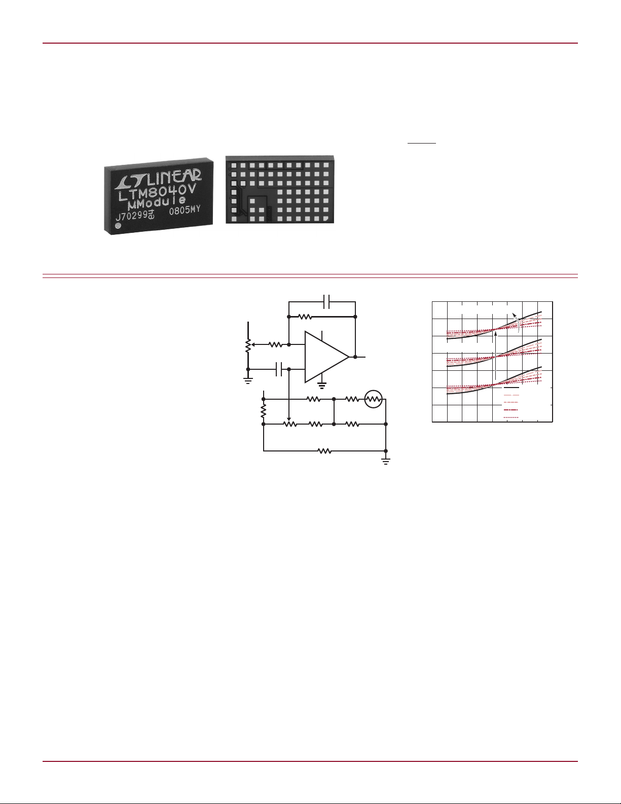
Figure 12. Thermistor-based application
circuit for static gain adjust and temperature
gain slope compensation. Adjust R1 and R2
as needed and route output to –VG control
terminal of the LTC6412.
ness, so the baseband processor can
continue its demodulation/decoding
operation without interruption. Most
digital VGAs produce unacceptable
signal discontinuities. The DAC does
have a glitch of its own, but it is a
baseband glitch that can be smoothed
with filters. The glitch in many digital
VGAs has no such remedy.
Gain and Temperature
Compensation
Many communication receivers require frequent gain optimization, but
others are designed with over-performing ADCs that can tolerate moderate
signal amplitude variation and avoid
much of the AGC hardware problem.
However, even these “fixed gain”
system blocks often require a gain
30
30
adjustment to compensate gain drift
overtemperature and any cumulative
gain tolerance of the other components. Several system components are
cascaded to form a chain that usually
includes a VGA to perform a one-time
adjustment of gain and temperature
slope to compensate the tolerances and
slopes of the other components. In this
scenario, the required temperature
and compensation information is not
known to the baseband processor or
it is impractical to send this data to a
suitably located VGA.
natural solution for this application
because it can easily interpret the output of most temperature transducers
without digitization. Figure 10 shows
An analog-controlled VGA is a
to illustrate the capabilities of the
LTM8040—this frequency is too low
for practical pulse width modulation,
being well within the discrimination
range of the human eye.
The LTM8040 also features a low
power shutdown state. When the
SHDN pin is active low, the input
quiescent current is less than 1µA.
Conclusion
The LTM8040 µModule LED driver
makes it easy to drive LEDs. Its high
level of integration and rich feature set,
including open LED protection, analog
and PWM dimming, save significant
design time and board space.
Figure 13. Gain vs temperature performance
characteristics of the thermistor-based circuit
shown in Figure 12
L
a simple application circuit using a
common PTAT temperature sensor
and an op amp to create the required
–VG signal to adjust room temperature
gain and temperature slope as shown
in Figure 11. If temperature slope
accuracy is only important for T >
0°C, then the same function can be
performed with an inexpensive NTC
thermistor as shown in Figures 12 and
13. Trying doing that with a digitally
controlled VGA!
Conclusion
By combining the advanced SiGe
process with an innovative design, the
LTC6412 offers unparalleled analog
VGA performance at 3.3V. The tiny
16mm² leadless package and minimal
external components produce a cost
effective, fully differential VGA solution
in less than 1cm² of PCB area.
Linear Technology Magazine • September 2009
L
 Loading...