

OUTPUT
V
REG
IC REGULATOR
REF
GND
VINSWITCH PIN
SWITCH
CONTROL
FEEDBACK NODE
+V
OUTPUT
V
REG
IC REGULATOR
REF
GND
V
IN
SWITCH
PIN
SWITCH
CONTROL
FEEDBACK NODE
+V
STEP-UP STEP-DOWN
AN122 F02
DIODE TURN-ON TIME
DIODE ON VOLTAGE
IC BREAKDOWN LIMIT
AN122 F03
DIODE
UNDER
TEST
5Ω
MEASUREMENT POINT
PULSE IN
t
RISE
≤ 2ns
AMPLITUDE = 5V + V
FWD
L DESIGN IDEAS
Diode Turn-On Time Induced
Failures in Switching Regulators
Never Has So Much Trouble Been Had
by So Many with So Few Terminals
by Jim Williams and David Beebe
This article is excerpted from the Linear
Technology Application Note AN122
with the same title.
Introduction
Most circuit designers are familiar with
diode dynamic characteristics such
as charge storage, voltage dependent
capacitance and reverse recovery
time. Less commonly acknowledged
and manufacturer specified is diode
forward turn-on time. This parameter
describes the time required for a diode
to turn on and clamp at its forward voltage drop. Historically, this extremely
short time, units of nanoseconds, has
been so small that user and vendor
alike have essentially ignored it. It
is rarely discussed and almost never
specified. Recently, switching regulator clock rate and transition time have
become faster, making diode turn-on
time a critical issue. Increased clock
rates are mandated to achieve smaller
magnetics size; decreased transition
times somewhat aid overall efficiency
but are principally needed to minimize
IC heat rise. At clock speeds beyond
about 1MHz, transition time losses are
the primary source of die heating.
A potential difficulty due to diode
turn-on time is that the resultant
Figure 2. Diode forward turn-on time permits transient excursion above
nominal diode clamp voltage, potentially exceeding IC breakdown limit.
34
34
transitory “overshoot” voltage across
the diode, even when restricted to
nanoseconds, can induce overvoltage
stress, causing switching regulator
IC failure. As such, careful testing is
required to qualify a given diode for a
particular application to insure reliability. This testing, which assumes
low loss surrounding components
and layout in the final application,
measures turn-on overshoot voltage
due to diode parasitics only. Improper
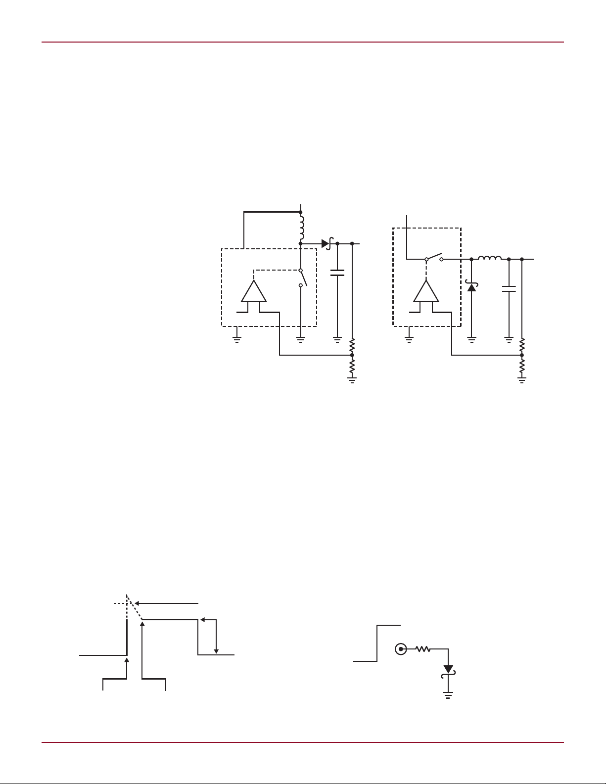
Figure 1. Typical voltage step-up/step-down converters. Assumption
is diode clamps switch pin voltage excursion to safe limits.
associated component selection and
layout will contribute additional overstress terms.
Diode Turn-On Time
Perspectives
Figure 1 shows typical step-up and
step-down voltage converters. In both
cases, the assumption is that the diode
clamps switch pin voltage excursions
to safe limits. In the step-up case, this
limit is defined by the switch pins
Figure 3. Conceptual method tests diode turn-on time at 1A. Input
step must have exceptionally fast, high fidelity transition.
Linear Technology Magazine • March 2009
DESIGN IDEAS L
AN122 F05
LT1086
22µF22µF
120Ω
1k
1k
+V ADJUST (RISE TIME TRIM)
+V TYPICAL 17VVIN = 20V
*
+V
Q1
Q4
+V
Q2
Q5
+V
Q3
Q6
1Ω
1Ω
1Ω
5Ω**
OUTPUT
62Ω50Ω
2pF TO 12pF
EDGE
PURITY
EDGE PURITY
100Ω
PULSE
INPUT
MINIMIZE INDUCTANCE IN ALL PATHS
= 2N3866
= 2N3375
** = TEN PARALLELED 50Ω RESISTORS
* = BYPASS EVERY TRANSISTOR WITH
22µF SANYO OSCON PARALLELED WITH
2.2µF MYLAR
+
+
*
*
1V/DIV
2ns/DIV
AN122 F06
AN122 F04
DIODE
UNDER
TEST
5Ω
OSCILLOSCOPE
1GHz BANDWIDTH
t
RISE
= 350ps
PULSE CURRENT
AMPLIFIER
t
RISE
= 2ns
PULSE GENERATOR
t
RISE
< 1ns
Z0 PROBE
≈1A
TYPICALLY
5V TO 6V, 30ns
WIDE
Figure 4. Detailed measurement scheme indicates necessary performance parameters for various elements. Subnanosecond rise time pulse
generator, 1A, 2ns rise time amplifier and 1GHz oscilloscope are required.
maximum allowable forward voltage.
The step-down case limit is set by
the switch pins maximum allowable
reverse voltage.
a finite length of time to clamp at its
forward voltage. This forward turnon time permits transient excursions
above the nominal diode clamp voltage, potentially exceeding the IC’s
breakdown limit. The turn-on time is
typically measured in nanoseconds,
making observation difficult. A further
complication is that the turn-on overshoot occurs at the amplitude extreme
of a pulse waveform, precluding high
resolution amplitude measurement.
These factors must be considered
when designing a diode turn-on test
method.
Linear Technology Magazine • March 2009
Figure 5. Pulse amplifier includes paralleled, darlington driven RF transistor output stage. Collector voltage adjustment
(“rise time trim”) peaks Q4 to Q6 FT, input RC network optimizes output pulse purity. Low inductance layout is mandatory.
Figure 2 indicates the diode requires
Figure 3 shows a conceptual method
for testing diode turn-on time. Here,
the test is performed at 1A although
other currents could be used. A pulse
Figure 6. Pulse amplifier output into 5Ω. Rise time is 2ns with minimal pulse-top aberrations.
steps 1A into the diode under test via
the 5Ω resistor. Turn-on time voltage excursion is measured directly
at the diode under test. The figure
3535

L DESIGN IDEAS
AN122 F05
LT1086
22µF22µF
120Ω
1k
1k
+V ADJUST (RISETIME TRIM)
+V, TYPICAL 17VV
IN
= 20V
*
+V
Q1
Q4
+V
Q2
Q5
+V
Q3
Q6
1Ω
1Ω
1Ω
5Ω**
DIODE
UNDER
TEST
62Ω50Ω
2pF TO 12pF
EDGE
PURITY
EDGE PURITY
100Ω
HP-215A
PULSE GENERATOR
t
RISE
= 800ps
P
WIDTH
= 30ns
MINIMIZE INDUCTANCE IN ALL PATHS
= 2N3866
= 2N3375
** = TEN PARALLELED 50Ω RESISTORS
* = BYPASS EVERY TRANSISTOR WITH
22µF SANYO OSCON PARALLELED WITH
2.2µF MYLAR
ADJUST PULSE GENERATOR AMPLITUDE FOR 5.5V AMPLITUDE AT 5Ω RESISTOR
Z
0
PROBE = TEKTRONIX
P-6056, 500Ω
215A
≈
6.7V
≈
5.5V
7104
7A29 7B15 7B107A29
TEKTRONIX
7104/7A29/7B10/7B15
1GHz (t
RISE
= 350ps)
OSCILLOSCOPE
+
+
*
*
Figure 7. Complete diode forward turn-on time measurement arrangement includes subnanosecond rise time
pulse generator, pulse amplifier, Z0 probe and 1GHz oscilloscope.
36
36
Linear Technology Magazine • March 2009

DESIGN IDEAS L
200mV/DIV
2ns/DIV
AN122 F08
200mV/DIV
2ns/DIV
AN122 F09
200mV/DIV
5ns/DIV
AN122 F12
200mV/DIV
2ns/DIV
AN122 F10
200mV/DIV
5ns/DIV
AN122 F11
Figure 8. “Diode Number 1” overshoots steady state
forward voltage for ≈3.6ns, peaking 200mV.
Figure 10. “Diode Number 3” peaks 1V above nominal
400mV VFWD, a 2.5x error.
Figure 9. “Diode Number 2” peaks ≈750mV before settling
in 6ns... > 2x steady state forward voltage.
Figure 11. “Diode Number 4” peaks ≈750mV with lengthy
(note horizontal 2.5x scale change) tailing towards VFWD value.
Figure 12. “Diode Number 5” peaks offscale with extended tailing (note
horizontal slower scale compared to Figures 8 thru 10).
Linear Technology Magazine • March 2009
3737

L DESIGN IDEAS
90
70
50
EMISSIONS LEVEL (dBµV/m)
30
10
80
60
40
20
0
–10
0 100 200 300 400 500
FREQUENCY (MHz)
600 700 800 900 1000
EN55022
CLASS B
LIMIT
90
70
50
EMISSIONS LEVEL (dBµV/m)
30
10
80
60
40
20
0
–10
0 100 200 300 400 500
FREQUENCY (MHz)
600 700 800 900 1000
EN55022
CLASS B
LIMIT
Authors can be contacted
at (408) 432-1900
is deceptively simple in appearance.
In particular, the current step must
have an exceptionally fast, high-fidelity
transition and faithful turn-on time
determination requires substantial
measurement bandwidth.
Detailed Measurement
Scheme
A more detailed measurement scheme
appears in Figure 4. Necessary performance parameters for various
elements are called out. A subnanosecond rise time pulse generator, 1A,
2ns rise time amplifier and a 1GHz
oscilloscope are required. These specifications represent realistic operating
conditions; other currents and rise
times can be selected by altering appropriate parameters.
The pulse amplifier necessitates
careful attention to circuit configuration and layout. Figure 5 shows the
amplifier includes a paralleled, Darlington driven RF transistor output
stage. The collector voltage adjustment
(“rise time trim”) peaks Q4 to Q6 FT;
an input RC network optimizes output
pulse purity by slightly retarding input
pulse rise time to within amplifier
passband. Paralleling allows Q4 to Q6
to operate at favorable individual currents, maintaining bandwidth. When
the (mildly interactive) edge purity and
rise time trims are optimized, Figure
6 indicates the amplifier produces a
transcendently clean 2ns rise time
output pulse devoid of ringing, alien
components or post-transition excursions. Such performance makes diode
turn-on time testing practical.
1
Figure 7 depicts the complete diode
forward turn-on time measurement arrangement. The pulse amplifier, driven
by a sub-nanosecond pulse generator,
drives the diode under test. A Z0 probe
monitors the measurement point and
feeds a 1GHz oscilloscope.
2, 3, 4
Diode Testing and
Interpreting Results
The measurement test fixture, properly equipped and constructed,
permits diode turn-on time testing
with excellent time and amplitude
resolution.5 Figures 8 through 12
show results for five different diodes
from various manufacturers. Figure 8
(Diode Number 1) overshoots steady
state forward voltage for 3.6ns, peaking
200mV. This is the best performance
of the five. Figures 9 through 12 show
increasing turn-on amplitude and
time which are detailed in the figure
captions. In the worst cases, turn-on
amplitudes exceed nominal clamp
voltage by more than 1V while turn-on
times extend for tens of nanoseconds.
Figure 12 culminates this unfortunate
parade with huge time and amplitude
errors. Such errant excursions can and
will cause IC regulator breakdown and
failure. The lesson here is clear. Diode
turn-on time must be characterized
and measured in any given application
to insure reliability.
Notes
1
An alternate pulse generation approach appears in
Linear Technology Application Note 122, Appendix
F, “Another Way to Do It.”
2
Z0 probes are described in Linear Technology Ap-
plication Note 122 Appendix C, “About Z0 Probes.”
See also References 27 thru 34.
3
The subnanosecond pulse generator requirement
is not trivial. See Linear Technology Application
Note 122 Appendix B, “Subnanosecond Rise Time
Pulse Generators For The Rich and Poor.”
4
See Linear Linear Technology Application Note
122 Appendix E, “Connections, Cables, Adapters,
Attenuators, Probes and Picoseconds” for relevant
commentary.
5
See Linear Technology Application Note 122 Ap-
pendix A, “How Much Bandwidth is Enough?” for
discussion on determining necessary measurement
bandwidth.
L
LTM8032, continued from page 33
amount of ambient noise in the room.
Figure 3 shows the noise spectrum in
the chamber without any devices running. This can be used to determine the
actual noise produced by the DUT.
Figure 4 shows the worst case
LTM8032 emissions plot, which occurs at maximum power out, 10V at
38
38
2A, from the maximum input voltage,
36V. There are two traces in the plot,
one for the vertical and horizontal
orientations of the test lab’s receiver
antenna. As shown in the figure, the
LTM8032 easily meets the CISPR 22
Conclusion
The LTM8032 switching step-down
regulator is both easy to use and quiet,
meeting the radiated emissions requirements of CISPR22 and EN55022
class B by a wide margin.
L
class B limits, with 20db of margin for
most of the frequency spectrum, with
either antenna orientation.
Figure 3. The baseline measurement of ambient
noise in the 5-meter chamber (no devices operating) Figure 4. The LTM8032 emissions for 20W out, 36V
IN
Linear Technology Magazine • March 2009
 Loading...