

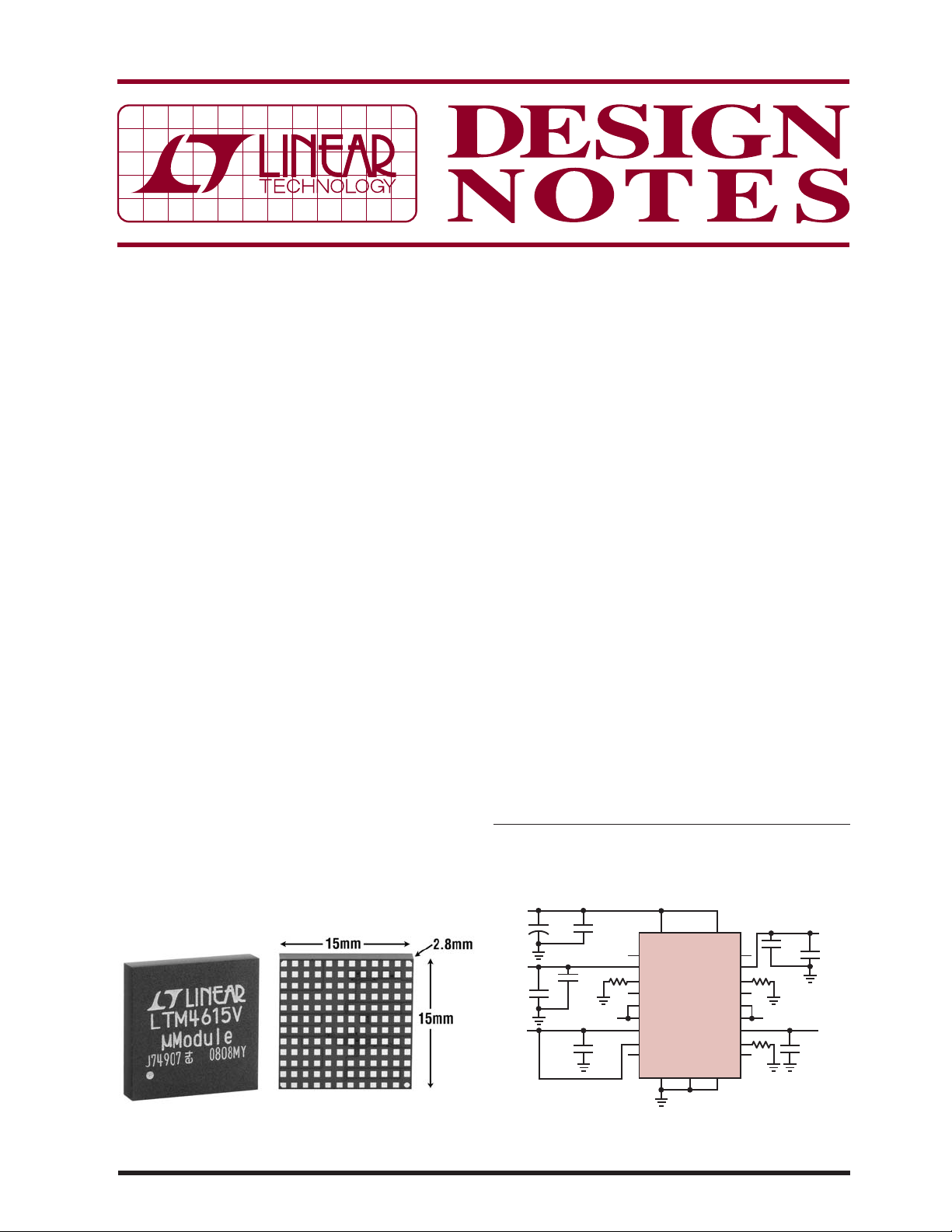
Triple Output DC/DC µModule® Regulator in 15mm × 15mm ×
2.8mm Surface Mount Package Replaces Up to 30 Discrete
Components Design Note 469
Eddie Beville and Alan Chern
Introduction
When space and design-time are tight in multivoltage
systems, the solution is a multioutput DC/DC regulator
IC. For more space and time constraint systems, a better
solution is an already-fabricated compact multioutput
DC/DC system that includes not only the regulator ICs
but the supporting components such as the inductors,
compensation circuits, capacitors and resistors.
Dual Switching 4A and 1.5A VLDO™ Regulators
The LTM®4615 offers three separate power supply
regulators in a 15mm × 15mm × 2.8mm LGA surface
mount package: two switching DC/DC regulators and
one very low dropout VLDO linear regulator (Figure 1).
MOSFETs, inductors, and other support components are
all built in. Each power supply can be powered indiv idually
or together, to form a single input, three output design.
Moreover, for an otherwise complex triple output circuit
design, the task is e ased to designing with only one device
while the layout is as simple as copying and pasting the
LTM4615’s package layout. One LTM4615 replaces up to
30 discrete component s when compared to a triple-output
high effi ciency DC/DC circuit.
The two switching regulators, operating at a 1.25MHz
switching frequenc y, accept input volt ages between 2.35 V
to 5.5V and each delivers a resistor-set output voltage
of 0.8V to 5V at 4A of continuous current (5A peak). The
output voltages can track each other or another voltage
source. Other features include, low output voltage ripple
and low thermal dissipation.
The VLDO regulator input voltage (1.14V to 3.5V) is capable of up to 1.5A of output current with an adjustable
output range of 0.4V to 2.6V, also via a resistor. The VLDO
regulator has a low voltage dropout of 200mV at maximum load. The regulator can be used independently, or
in conjunction with either of the two switching regulators
to create a high effi ciency, low noise, large-ratio stepdown supply— simply tie one of the switching regulator’s
outputs to the input of the VLDO regulator.
Multiple Low Noise Outputs
The LTM4615 is capable of operating with all three regulators at full load while maintaining optimum effi ciency.
A typical LTM4615 design (Figure 2) for a 3.3V input to
three outputs has the VLDO input driven by V
OUT2
. The
effi ciency of this design is shown in Figure 3.
L, LT, LTC, LTM, Linear Technology, the Linear logo and μModule are registered
trademarks, and VLDO is a trademark of Linear Technology Corporation.
All other trademarks are the property of their respective owners.
V
IN
3.3V
V
OUT1
1.8V, 4A
V
OUT2
+
C2
82μF
C7
22μF
C6
100μF
C1
10μF
s2
C3
10μF
V
R2
4.02k
IN
V
IN1
PGOOD1
V
OUT1
FB1
COMP1
TRACK1
RUN/SS1
LDO_IN
EN3
BOOST3
GND1
LTM4615
GND2
V
IN2
PGOOD2
V
OUT2
FB2
COMP2
TRACK2
RUN/SS2
LDO_OUT
FB3
PGOOD3
GND3
3.32k
DN469 F02
10k
V
OUT2
1.2V, 4A
C4
C5
22μF
C8
4.7μF
100μF
V
OUT3
1V, 1.5A
R4
V
IN
R1
Figure 1. Three DC/DC Circuits in One Package
08/09/469
Figure 2. Triple Output LTM4615: 3.3V Input,
1.8V (4A), 1.2V (4A), 1.0V (1.5A)
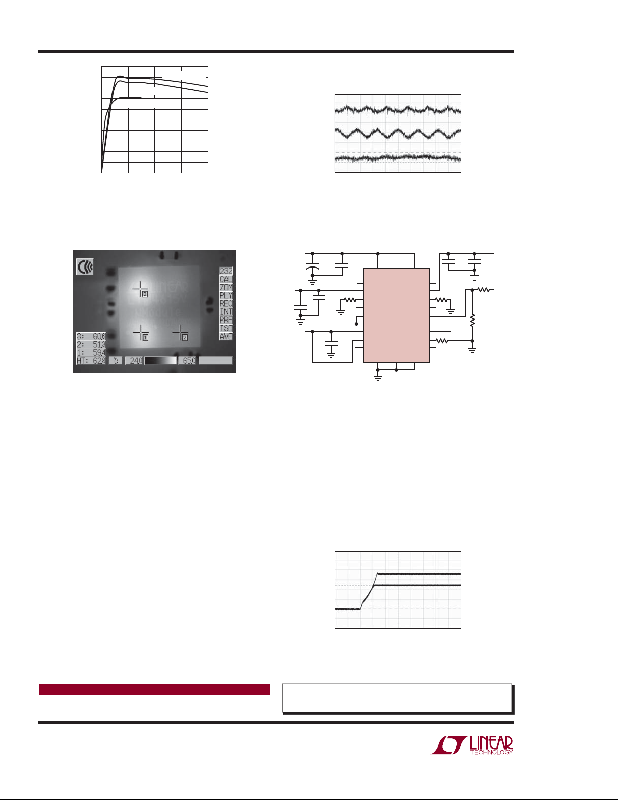
100
90
80
70
60
50
40
EFFICIENCY (%)
30
20
10
0
0
3.3VIN TO 1.2V
1.2VIN TO 1.0V
OUTPUT CURRENT (A)
3.3VIN TO 1.8V
OUT
2
OUT
OUT
DN469 F03
1.8V
1.2V
1.0V
431
0.5μs/DIV
DN469 F04
1.6mV
2.0mV
1.4mV
P-P
P-P
P-P
Figure 3. Effi ciency of the Circuit in Figure 2,
1.8V, 1.2V and 1.0V (VLDO)
Figure 5. Top View Thermal Imaging of the Unit at Full
Load in Ambient Temperature with No Airfl ow. Even
Temperatures (Cursors 1 and 3) Indicate Balanced
Thermal Conductivity Between the Two Switching
Regulators. 3.3V Input, 1.8V (4A) and 1.2V (4A).
The LTM4615 comes prepackaged with ceramic capacitors and additional output capacitors are only needed
under full 4A load and if the input source impedance is
compromised by long inductive leads or traces.
The VLDO regul ator provides a particular ly low noise 1.0V
supply as it is driven by the output of the 1.2V switching
regulator (V
). The low output voltage ripple for all
OUT2
three outputs is shown in Figure 4.
Thermally Enhanced Packaging
The LGA packaging allows heatsinking from both the top
and bottom. This design utilizes the PCB copper layout
to draw heat away from the part and into the board. Additionally, a heat sink can be placed on top of the device,
such as a metal chassis, to promote thermal conduc tivity.
Thermal dissipation is well balanced between the two
switching regulators (Figure 5).
Figure 4. Low Output Voltage Ripple (3.3V Input)
4.99k
R6
10k
C5
100μF
R5
V
OUT2
1.2V, 4A
V
OUT1
V
OUT1
1.8V,
2.5V to
5.5V
4A
V
OUT2
V
IN
+
C2
82μFC110μF
C6
100μF
C7
22μF
V
C3
10μF
R2
4.02k
IN
C4
10k
3.32k
DN469 F06
22μF
R4
V
V
IN
OUT3
1V,
R1
1.5A
V
IN1
s2
PGOOD1
V
OUT1
FB1
COMP1
TRACK1
RUN/SS1
LDO_IN
EN3
BOOST3
GND1
LTM4615
GND2
V
IN2
PGOOD2
V
OUT2
FB2
COMP2
TRACK2
RUN/SS2
LDO_OUT
FB3
PGOOD3
GND3
Figure 6. Output Voltage Tracking Design
V
(1.2V) Tracks V
OUT2
OUT1
(1.8V)
Output Voltage Tracking
A tracking design (Figure 6) and output (Figure 7) can be
programmed using the TRACK1 and TRACK2 pins. Divide
d o w n t h e m a s t e r r e g u l a t o r ’ s o u t p u t w i t h a n e x t e r n a l r e s i s t o r
divider that is the same as the slave regulator’s feedback
divider on the slave’s TRACK pin for coincident tracking.
1.8V
OUT1
1.2V
OUT2
0.5V/DIV
Figure 7. Start-Up Voltage for Figure 5 Circuit V
Coincidentally Tracks V
(1.2V) for Coincident Tracking
OUT2
DN469 F07
OUT1
(1.8V)
Data Sheet Download
www.linear.com
Linear Technology Corporation
1630 McCarthy Blvd., Milpitas, CA 95035-7417
(408) 432-1900
●
FAX: (408) 434-0507 ● www.linear.com
For applications help,
call (408) 432-1900, Ext. 2593
dn469f LT/TP 0809 116K • PRINTED IN THE USA
© LINEAR TECHNOLOGY CORPORATION 2009
 Loading...