


Step-Down µModule Regulator Produces 15A Output from
Inputs Down to 1.5V—No Bias Supply Required
1.5V to 5.5V Input, 0.8V to 5V Output from a 15mm × 15mm × 4.32mm LGA Package
Design Note 488
Alan Chern and Jason Sekanina
15A High Efficiency Output from a Low Input Voltage
The LTM®4611 is a switch mode, step-down DC/DC µModule
regulator in a compact 15mm × 15mm × 4.32mm LGA surface
mount package. The switching controller, MOSFETs, inductor
and supporting components are housed in the package. With
a built-in differential remote sense amplifier, the LTM4611 can
tightl y regulate its ou tput voltage fr om 0.8V to within 300 mV of
VIN and deliver 15A output efficiently from 1.5V to 5.5V input.
Only a handful of components are needed to create a complete
point-of-load (POL) solution with the LTM4611 (see Figure 1).
The CSS capacitor provides smooth start-up on the output
and limits the input surge current during power-up. CFF and
CP set the loop-compensation for fast transient response
and good stability. The output voltage, 1.5V, is set by a single
resistor, R
SET
.
Efficiency is exceptional, even down to the lowest input voltages, as shown in Figure 2.
®
Input and Output Ripple
Output capacitors should have low ESR to meet output voltage ripple and transient requirements. A mixture of low ESR
polymer and/or ceramic capacitors is sufficient for producing low output ripple with minimal noise and spiking. Output
capacitors are chosen to optimize transient load response and
loop st ability to mee t the applicat ion load-step r equirements
by
using the E xcel-based LTpowerCAD™ des ign tool. (Table 5 of the
LTM4611 data sheet prov ides guidance for a pplications wi th 7.5 A
L, LT, LTC, LTM, Linear Technology, the Linear logo and µModule are registered
trademarks and LTPowerCAD is a trademark of Linear Technology Corporation.
All other trademarks are the property of their respective owners.
Scan this code with your
smart phone or click to view
informative videos.
QR code
m.linear.com/4611
Download a QR code reader application to scan
and read QR codes from your phone.
V
IN
1.8V TO
5.5V
680µF
18mΩ ESR
2× 47µF
95
90
85
80
75
70
EFFICIENCY (%)
65
60
55
C
SS
0.1µF
TRACK/SS
RUN
MODE_PLLIN
Figure 1. 1.8V
V
IN
LTM4611
V
DIFFV
SGND GND
to 5.5VIN to 1.5V
IN
PGOOD
V
OUT
V
OUT_LCL
OUT
V
OSNS
V
OSNS
FB
+
–
CP*
with 15A Output Load Current
1.8V TO 1.5V
2.5V TO 1.5V
3.3V TO 1.5V
5V TO 1.5V
10 12 16
0
2 64
8 14
OUTPUT CURRENT (A)
Figure 2. Efficiency of
Figure 1 Circuit
video.linear.com/56
DN488 F01
*OPTIONAL
OUT
DN488 F02
C
47pF
R
SET
69kΩ
V
OUT
1.5V
FF
15A
100µF
×4
03/11/488
SWITCH
V
RIPPLE
V
OUT
RIPPLE
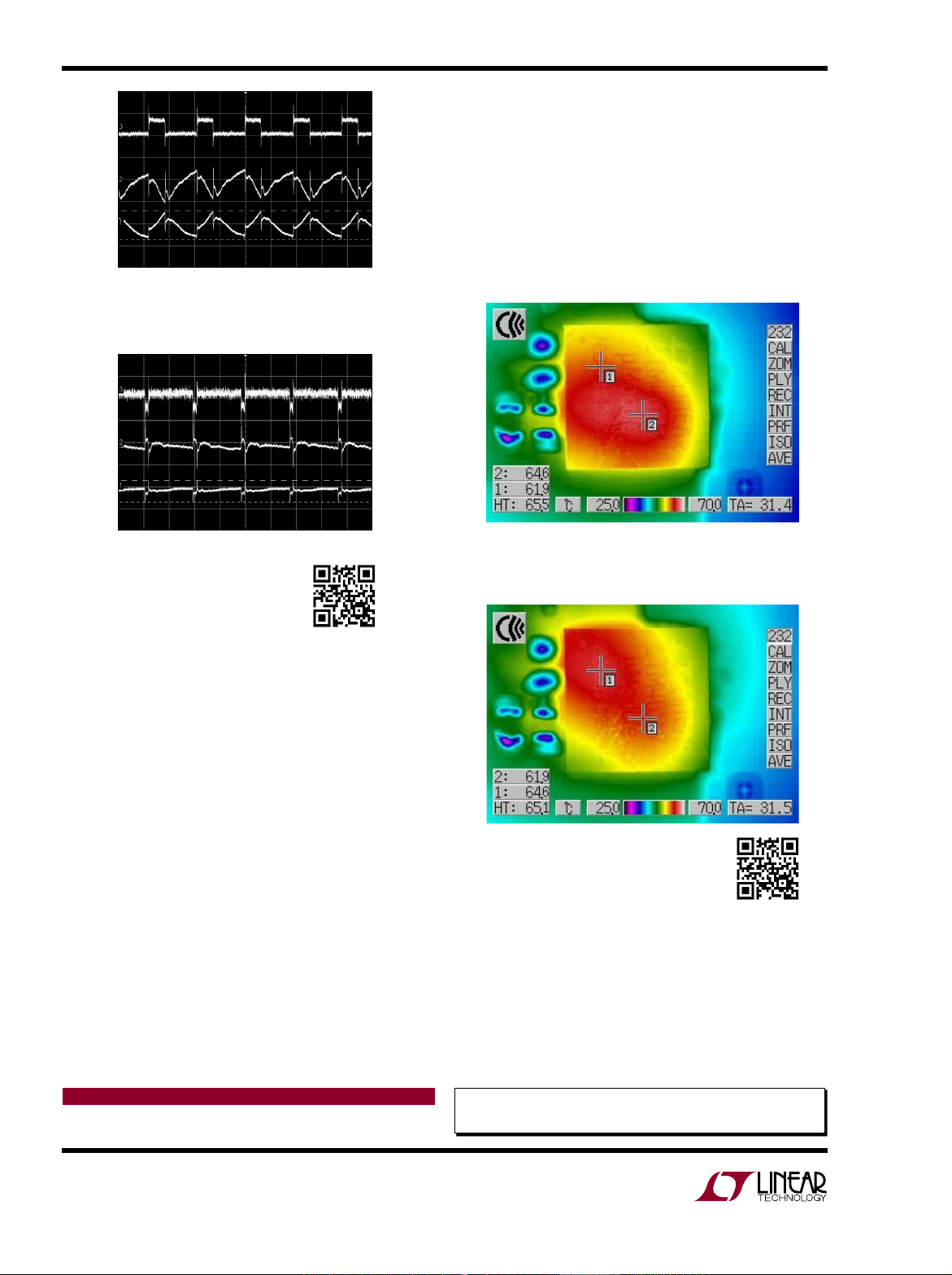
dissipation with or without air flow. Figure 5 shows the top
view thermal imaging of the LTM4611 at a power loss of 3.5W
50mV/DIV
with no air flow, when converting 5V to 1.5V.
Internal self-heating of the LTM4611 remains quite low even at a
IN
50mV/DIV
low 1.8V input voltage due to its micropower bias generator that
enables s trong gate driv e for its power MOSFE Ts. Figure 6 show s
20mV/DIV
a power loss of 3.2W with hot spots slightly changed from their
positions with a 5V input—the nominal surface temperature is
60°C. Watch the associated videos to see the test set-up and
1µs/DIV
DN488 F03
watch 200 LFM of air flow cool the unit by 10°C.
Figure 3. 5VIN to 1.5V
SWITCH
V
IN
RIPPLE
V
OUT
RIPPLE
Figure 4. 1.8V
1µs/DIV
to 1.5V
IN
at 15A Output Load
OUT
DN488 F04
OUT
20mV/DIV
50mV/DIV
20mV/DIV
at 15A Output Load
video.linear.com/57
load-steps and 1µs transition times.) For this design example,
four 100µF ceramic capacitors are used. Figures 3 and 4 show
input and out put ripple at 15A load with 2 0MHz bandwidth -limit.
View the associated videos to see the test methodology, as well
as ripple waveforms without bandwidth limiting.
For this design, the choice of input capacitors is critical due
to the low input voltage range. Long input traces can cause
voltage drops, which could nuisance-trip the µModule regulator’s undervoltage lockout (UVLO) detection circuitry. Input
ripple, t ypically a non -issue with higher in put voltages, m ay fall
a significant percentage below nominal—close to UVLO—at
lower input voltages. In this case, input voltage ripple should
be addressed since input filter oscillations can occur due to
poor damping under heavy load current. This design uses a
large 6 80µF POSCAP an d two 47µF ceramic cap acitors to compensat e for meter-long input cables u sed during bench tes ting.
Thermally Enhanced Packaging
The device’s LGA packaging allows heat sinking from both
the top and bottom, facilitating the use of a metal chassis or
a BGA heat sink. This form factor promotes excellent thermal
Figure 5. 5VIN to 1.5V
at 15A Output Load.
OUT
3.5W Power Loss with 0LFM and 65°C Surface
Temperature Hot Spot
Figure 6. 1.8VIN to 1.5V
OUT
at 15A
Output Load. 3.2W Power Loss
with 0LFM and 65°C Surface
Temperature Hot Spot
video.linear.com/55
Conclusion
The LTM4611 is a step-down µModule regulator that easily
fits into POL applications needing high output current from
low voltage inputs—from 1.5V to 5.5V. Efficiency and thermal
perf ormance remain hi gh across the entir e input voltage r ange,
simplifying electrical, mechanical and system design in data
storage, RAID, ATCA, and many other applications.
Data Sheet Download
www.linear.com/4611
Linear Technology Corporation
1630 McCarthy Blvd., Milpitas, CA 95035-7417
(408) 432-1900
●
FAX: (408) 434-0507 ● www.linear.com
For applications help,
call (408) 432-1900, Ext. 2593
dn488f LT/AP 0311 226K • PRINTED IN THE USA
LINEAR TECHNOLOGY CORPORATION 2011
 Loading...