

LINEAR TECHNOLOGY
LINEAR TECHNOLOGY
LINEAR TECHNOLOGY
MARCH 2009 VOLUME XIX NUMBER 1
SPI
CURRENT
SENSOR
SERVICE SWITCH
CAN
12-CELL BATTERY
MODULE
–
–
DATA BUS
+
+
BATTERY
MONITORING
& BALANCING
HOST
CONTROLLER
–
+
–
+
–
+
–
+
–
+
–
+
–
+
12-CELL BATTERY
MODULE
DATA BUS
BATTERY
MONITORING
& BALANCING
12-CELL BATTERY
MODULE
DATA BUS
12-CELL BATTERY
MODULE
DATA BUS
12-CELL BATTERY
MODULE
DATA BUS
12-CELL BATTERY
MODULE
DATA BUS
12-CELL BATTERY
MODULE
DATA BUS
12-CELL BATTERY
MODULE
DATA BUS
BATTERY
MONITORING
& BALANCING
BATTERY
MONITORING
& BALANCING
BATTERY
MONITORING
& BALANCING
BATTERY
MONITORING
& BALANCING
BATTERY
MONITORING
& BALANCING
BATTERY
MONITORING
& BALANCING
IN THIS ISSUE…
COVER ARTICLE
Battery Stack Monitor
Extends Life of Li-Ion Batteries
in Hybrid Electric Vehicles ..................1
Michael Kultgen and Jon Munson
Linear in the News… ...........................2
DESIGN FEATURES
DC/DC Converter, Capacitor Charger
Takes Inputs from 4.75V to 400V ........9
Robert Milliken and Peter Liu
How to Choose a Voltage Reference ...14
Brendan Whelan
1.2A Monolithic Buck Regulator Shrinks Supply Size and Cost with Programmable Output Current Limit
.........................................................20
Tom Sheehan
Boost Converters for Keep-Alive Circuits
Draw Only 8.5µA of Quiescent Current
.........................................................22
Xiaohua Su
Industrial/Automotive Step-Down
Regulator Accepts 3.6V to 36V and
Includes Power-On Reset and Watchdog
Timer in 3mm × 3mm QFN ................24
Ramanjot Singh
Complete APD Bias Solution in 60mm
with On-the-Fly Adjustable Current
Limit and Adjustable V
Xin (Shin) Qi
...................27
APD
2
Battery Stack Monitor Extends Life of Li-Ion Batteries in Hybrid Electric Vehicles
by Michael Kultgen and Jon Munson
Introduction
The cost of running a car on electricity
is equivalent to paying $0.75/gallon
for gasoline, and if that electricity
comes from carbon neutral sources,
car owners are saving both money
and the environment (gasoline combustion produces 9kg of CO2 per US
gallon). Advancements in battery
technology (see sidebar), especially
with Lithium-based chemistries, hold
the greatest promise for converting
the worldwide fleet of cars to hybrid
or fully electric.
Lithium battery packs offer the
highest energy density of any cur rent battery technology, but high
performance is not guaranteed simply by design. In real world use, a
battery management system (BMS)
makes a significant difference in the
performance and lifetime of Li-Ion
batteries—arguably more so than
the design of the battery itself. The
LTC6802 multicell battery stack
monitor is central to any BMS for the
continued on page 3
DESIGN IDEAS
Don’t Want to Hear It? Avoid the Audio
Band with PWM LED Dimming at
Frequencies Above 20kHz ..................30
Eric Young
Eliminate EMI Worries with 2A,
15mm × 9mm × 2.82mm µModule™
Step-Down Regulator ........................33
David Ng
Diode Turn-On Time Induced Failures
in Switching Regulators ....................34
Jim Williams and David Beebe
µModule Regulator Fits a (Nearly)
Complete Buck-Boost Solution in
15mm × 15mm × 2.8mm for
4.5V–36V VIN to 0.8V–34V V
Judy Sun, Sam Young and Henry Zhang
New Device Cameos ...........................41
Design Tools ......................................43
Sales Offices .....................................44
..........39
OUT
L
, LT, LTC, LTM, Burst Mode, OPTI-LOOP, Over-The-Top and PolyPhase are registered trademarks of Linear Technology
Corporation. Adaptive Power, Bat-Track, BodeCAD, C-Load, DirectSense, Easy Drive, FilterCAD, Hot Swap, LinearView,
µModule, Micropower SwitcherCAD, Multimode Dimming, No Latency ΔΣ, No Latency Delta-Sigma, No R
Filter, PanelProtect, PowerPath, PowerSOT, SmartStart, SoftSpan, Stage Shedding, SwitcherCAD, ThinSOT, TimerBlox, True
Color PWM, UltraFast and VLDO are trademarks of Linear Technology Corporation. Other product names may be trademarks
of the companies that manufacture the products.
Figure 1. 96-cell battery pack
, Operational
SENSE
L LINEAR IN THE NEWS
Linear in the News…
EDN Highlights Linear for Innovation Awards
EDN magazine in February chose several Linear Technology
products as finalists for their annual Innovation Awards, to
be announced later this month. And the nominees are:
Best Contributed Article—“High Voltage,
Low-Noise DC/DC Converters” by Jim Williams
You can find the article in its entirety on the EDN website
at www.edn.com/jimwilliams.
Battery ICs Category—LTC6802 Battery Stack Monitor
The LTC6802 is a highly integrated multicell battery
monitoring IC capable of precisely measuring the voltages
of up to 12 series-connected battery cells. Using a novel
stacking technique, multiple LTC6802s can be placed in
series without optocouplers or isolators. See the cover
article of this issue for an overview of this part.
Power ICs Category—LTC3642 50mA
Synchronous Step-Down Converter
The LTC3642 uses a unique high voltage synchronous
rectification design, capable of continuous input voltages of 45V and offers transient protection up to 60V. Its
internal synchronous rectification and its programmable
peak current mode control feature enable it to deliver up
to 93% efficiency, maximizing battery run time.
Power ICs: Modules—LTM4606 Ultralow EMI,
6A DC/DC µModule Regulator
The LTM4606 DC/DC µModule™ regulator significantly
reduces switching regulator noise by attenuating conducted
and radiated energy at the source. The µModule device
is a complete DC/DC system-in-a-package, including the
inductor, controller IC, MOSFETs, input and output capacitors and the compensation circuitry, housed in an enclosed
surface-mount plastic package resembling an IC.
The LTM4606 reduces switching regulator noise at the source.
Linear CEO Comments on Growth Markets
Last month in EE Times, Linear Technology CEO Lothar
Maier discussed the challenging market conditions and
the bright spots on the horizon: “In these times our customers will continue to invest in new products and new
product development. Innovation will return growth to the
semiconductor market—specifically to analog. Now is the
time to get new products out, to be first to market and to
have products that target emerging growth markets.” He
discussed several key markets:
q
Automotive. “Automotive manufacturers are
forecasting automotive electronic content to grow 2–3
times over the next few years, so we will continue
to provide new products to the automotive area. In
addition, every major automotive manufacturer in the
world is now working on hybrid vehicles, which will
add even more electronic content in cars. We have
just introduced an innovative device, the LTC6802,
a highly integrated battery stack monitor that
significantly eases the design of battery monitoring
systems for hybrid/electric vehicles.”
q
Green Growth Markets. “Products targeted toward
energy conservation or energy harvesting will
see growth opportunities and are insulated from
the current market conditions. Energy costs and
environmental concerns, as well as the need to
extend battery life for mobile devices, have led to a
focus on power optimization. Our energy-efficient
products enable customers to convert power more
efficiently, consume less power and extend battery
life. Our LED drivers enable a new generation of
low power lighting for a range of applications, from
cars and medical instruments to laptops and office
lighting. Our efficient analog solutions will help drive
innovative cleantech markets such as solar and wind
power systems.”
q
Communications Infrastructure. “Wireless systems
continue to produce significant market opportunities
for products in wireless and network infrastructure.
Our high speed data converters and high frequency
products are designed into the next generation of
cellular basestations. And our Hot Swap™ and Power
over Ethernet products are proliferating in networks.”
q
Industrial. “The broad industrial market continues
to provide a solid core of business and is somewhat
more insulated from market swings. Linear’s analog
products are used in a broad range of industrial
systems, including factory automation, industrial
process control, medical, instrumentation and
security.”
Lothar Maier concluded, “Finally, I believe that Linear’s
strategy of customer, market and geographic diversity will
be a hedge against the current market conditions and will
provide the conduit to future growth.”
L
2
2
Linear Technology Magazine • March 2009
DESIGN FEATURES L
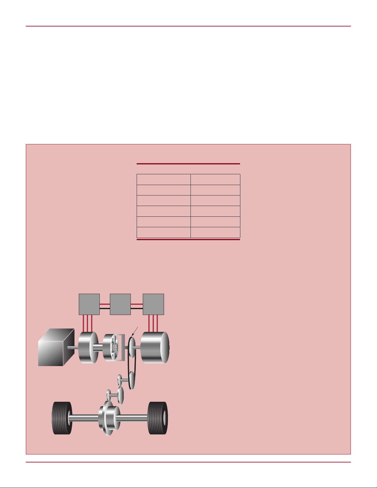
MG1 INVERTER MG2 INVERTERBATTERY
AXLES
DIFFERENTIAL
GASOLINE
ENGINE
ELECTRIC MOTOR/
GENERATOR 1 (MG1)
ELECTRIC MOTOR/
GENERATOR 2 (MG2)
POWER SPLIT
DEVICE
FRONT
WHEELS
REDUCTION
GEARS
SILENT
CHAIN
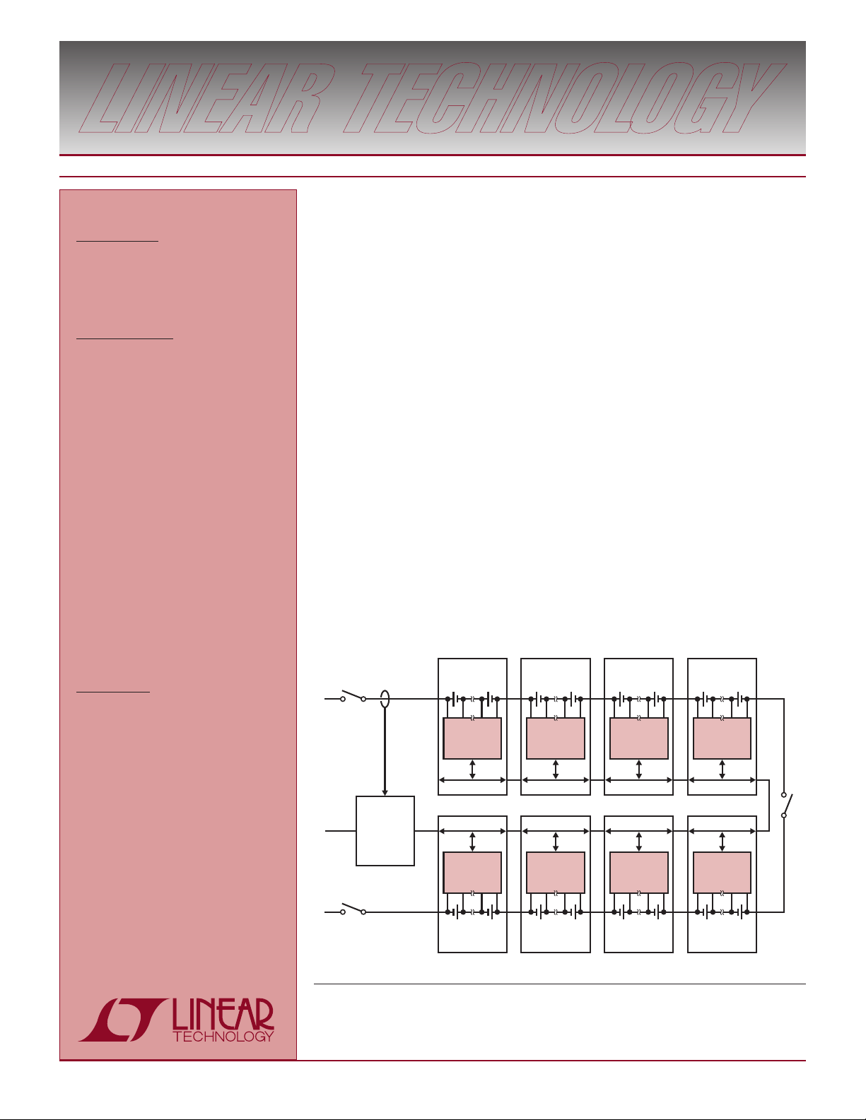
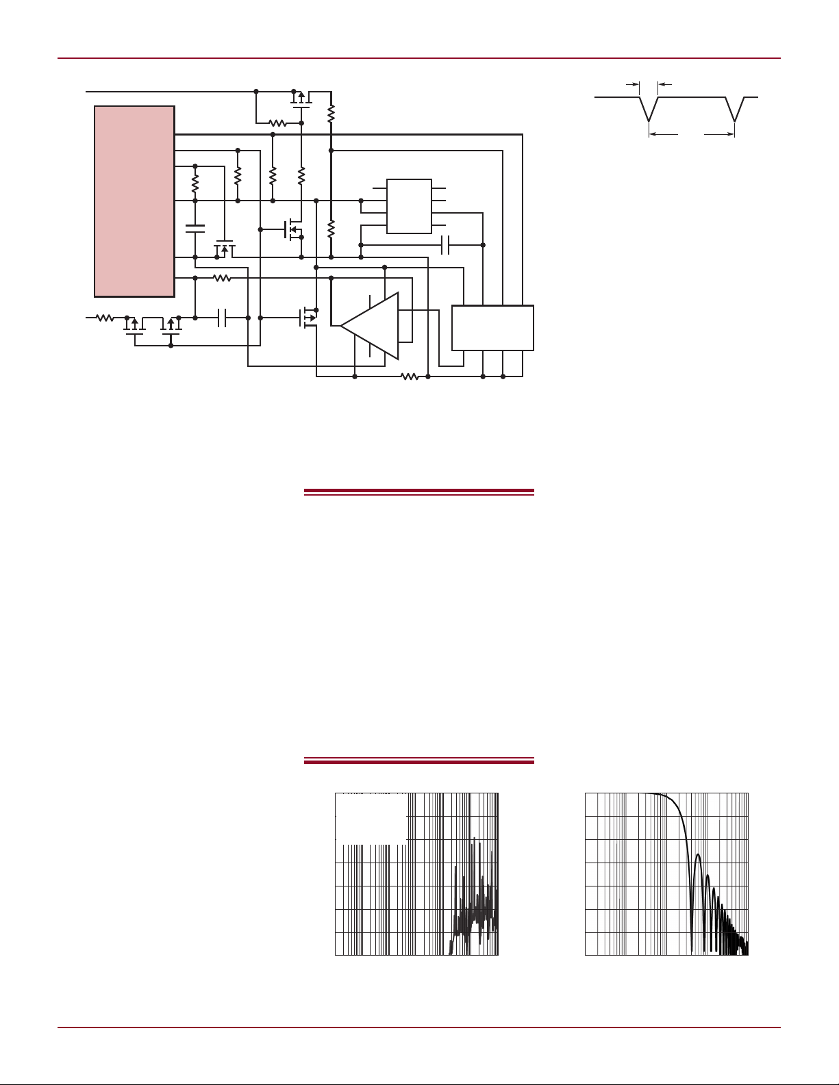
LTC6802, continued from page 1
large battery stacks common in electric vehicles (EVs) and hybrid electric
vehicles (HEVs). Its robust design and
high accuracy helps guarantee the
performance and lifetime of expensive
battery packs.
lifetime is traded against the need
to use as few kg of batteries as possible—the most expensive component
in any EV. Only a well-designed BMS
can maximize battery performance and
lifetime in the face 200A peak charge
and discharge currents.
For instance, to meet a 15-year,
5000 charge cycle goal, only a portion
(say 40%) of the battery pack’s cellcapacity can be used. Of course, using
only 40% of the capacity essentially
lowers the energy density of the pack.
This is the problem: increasing battery
Battery Management System
Optimizes Li-Ion Run Time
and Lifetime
In any battery stack, the more accurately you know state of charge (SOC)
of each cell, the more cell capacity you
Li-ion Batteries in Electric Vehicles and Hybrids
So why aren’t all cars electric? One
reason is energy density. Gasoline
holds 80 times the energy per kg as
Li-ion batteries (Table 1) and refuels
in three minutes, essentially allowing
indefinite driving. Even a big lithium
pack only gives a passenger car
about a 100-miles after an 8-hour
charging cycle. To drive a passenger
car further than 100 miles you still
need a gasoline engine, but even
so, batteries improve gas mileage in
hybrid electric vehicles (HEVs). The peak efficiency of
the Otto cycle engine is only 30% at high RPMs and the
average efficiency is about 12%. Using batteries to supply torque during acceleration and recover joules during
Figure 2. Toyota Prius “split power” hybrid drive train
Table 1. Energy density comparison
Medium Wh/kg
Diesel Fuel 12,700
Gasoline 12,200
Li-Ion Battery 150
NiMh Battery 100
Lead Acid Battery 25
Li-ion batteries take energy density another step forward,
by offering another 50% improvement. The safety of Liion was a concern, but new battery technologies like the
A123 nanophosphate cell, the EnerDel Spinel-Titanate
chemistry, the GS Yuasa EH6 design and others are as
safe as NiMh, offer extremely high power (200A peak discharge rates), and last 10 to 15 years with proper charge
management. By model year 2012, the majority of hybrid
cars and trucks will use lithium battery technology.
Figure 1 shows a shows a block diagram of the battery pack with a BMS, and Figure 2 shows a typical HEV
power train. The battery pack building block is a 2.5V
to 3.9V, 4Ahr to 40Ahr Li-ion cell. 100 to 200 cells are
connected in series to bring the battery pack voltage into
the hundreds of volts. This DC power source drives a
30kW to 70kW electric motor. The pack voltage is high
so that the average current is low for a given power level.
Lower current reduces I2R power losses, so cables can
be smaller, thus reducing weight and cost. The pack
should be able to deliver 200A under peak conditions
and be quickly rechargeable. In other words, the battery
needs to offer high energy density and high power density, specifications that can be met by Li-ion batteries.
Systems for busses and tractor-trailers use up to four
parallel packs of 640V each.
can use while still maximizing cell life.
In a laptop computer, gas gauging
comes from monitoring cell voltage
and counting coulombs in and out of
the stack of four to eight cells. Voltage, current, time and temperature
are combined in a robust algorithm
to give an indication of the SOC. Unfortunately, it’s nearly impossible to
count coulombs in a car. The battery
drives an electric motor, not a motherboard, so it must handle current
spikes of 200A, followed by low level
idling. Furthermore, you have from 96
regenerative braking means the gas
engine runs less often and runs at a
higher efficiency, effectively doubling
the mpg.
In the 1970s the only available high
power battery chemistry was lead
acid, too heavy to reasonably power
anything larger than a golf cart. Then
came NiMh batteries, which improved
energy density enough to enable the
first commercially successful HEVs,
like the Toyota Prius and Ford Escape.
L
Linear Technology Magazine • March 2009
3
L DESIGN FEATURES
DISCHARGE (%)
0
CELL VOLTAGE (V)
3.5
4.0
70
3.0
2.5
20 40
10 90
30 508060 100
2.0
1.5
4.5
1C
2C
5C
10C
20C
50C
DISCHARGE (%)
0
CELL VOLTAGE (V)
3.5
4.0
70
3.0
2.5
20 40
10 90
30 508060 100
2.0
1.5
4.5
–20°C
0°C
30°C
60°C
MEASUREMENT ERROR (%)
TEMPERATURE (°C)
125–50
0.30
–0.30
–25 0 25 50 75 100
–0.20
–0.25
–0.10
0.10
0
0.20
–0.15
–0.05
0.15
0.05
0.25
7 REPRESENTATIVE
UNITS
COST OF TYPICAL BATTERY PACK ($)
MEASUREMENT ERROR (mV)
300
9k
3k
5
10 15
20 25
4k
5k
7k
6k
8k
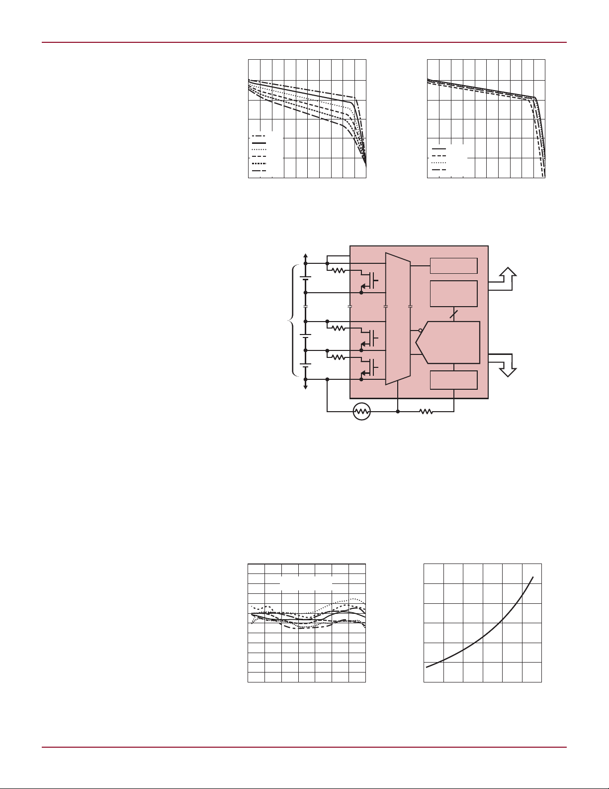
MUX
DIE TEMP
12-CELL
BATTERY
STRING
NEXT 12-CELL
PACK ABOVE
NEXT 12-CELL
PACK BELOW
V
+
V
–
100k NTC
100k
EXTERNAL
TEMP
SERIAL DATA
TO LTC6802-1
ABOVE
SERIAL DATA
TO LTC6802-1
BELOW
LTC6802-1
VOLTAGE
REFERENCE
REGISTERS
AND
CONTROL
12-BIT
∆∑ ADC
to 200 cells in series, in groups of 10
or 12. The cells age at different rates,
were manufactured from multiple lots,
and vary in temperature. Their capacities diverge constantly. Different cells
with the same coulomb count can have
wildly different charge levels.
That’s why the BMS focuses on
cell voltage. If you can accurately
measure the voltage of every cell, you
can know the cell’s SOC with reasonable accuracy (Figure 3). The trick is
to improve the accuracy of the voltage
measurement by taking into account
temperature effects on battery ESR
and capacity. By constantly measuring
each cell’s voltage, you keep a running
estimation of each cell’s charge level.
If some cells are overcharged and
some under, they can be balanced by
bleeding off charge (passive balancing) or redistributing charge (active
balancing).
Figure 3. State of charge vs current and temperature for a typical Li-ion cell
Accurate Monitoring is Key to
Raising Battery Performance
while Lowering Costs
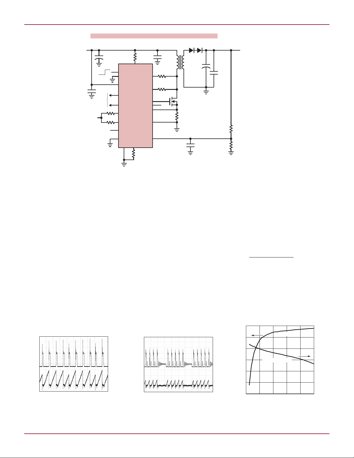
The LTC6802 (Figure 4) is a precision data acquisition IC optimized for
measuring the voltage of every cell in
a large string series-connected batteries. In the BMS, the LTC6802 does the
heavy lifting analog function, passing
digital voltage and temperature measurements to the host processor for
SOC computation. The LTC6802’s high
accuracy, excellent noise rejection,
high voltage tolerance, and extensive
self-diagnostics make it robust and
easy-to-use. The high level of integration means a substantial cost savings
for customers when compared to
discrete component data acquisition
designs.
Increasing measurement accuracy
reduces battery cost, as illustrated
by the following example. Figure 5
shows the typical performance of the
LTC6802, where 0.1% total error from
–20°C to 60°C translates to 4mV precision for a 3.7V cell. Suppose that to
achieve a 15-year battery lifetime, you
are limited to 40% of a cell’s capacity
per charge cycle, and assume the cell
voltage vs charge level of the battery
is very flat, e.g., 1.25mV/%SOC. A
measurement error of 4mV means the
4
Figure 4. Simplified block diagram of the LTC6802
estimation of SOC is accurate to 3%.
The BMS must charge cells to no more
than 37% (40% – 3%) of their capacity
to guarantee the 15-year lifetime.
Now consider a monitor IC with
10mV error over similar conditions.
In this case, the BMS can only use
Figure 5. Typical measurement accuracy
vs temperature of seven samples
32% (40% – 10mV • 1%/1.25mV) of
the cells’ capacity and still guarantee a
15-year life. This seemingly negligible
increase in measurement error results
in a significant 14% reduction in the
usable capacity. That is, a vehicle
requires least 14% more batteries, or
Figure 6. High BMS accuracy is important to
keeping battery costs in check, as shown in
this cost vs measurement error model.
Linear Technology Magazine • March 2009
LTC6802-1
GPIO2
V
−
C1
V
REG
GPIO1
0 = REF_EN
0 = CELL1
V
STACK12
CELL1
CELL12
1M
1M
2N7002
2N7002
TP0610K
TP0610K
TP0610K
TP0610K
1µF
WDTB
LT1461A-4
DNC
DNC
V
OUT
DNC
DNC
V
IN
SD
GND
1M 10M
1M
90.9k
150Ω
100Ω
2.2M
1M
100nF
2.2µF
4.096V
+
–
TC4W53FU
LT1636
SD
SELCH1CH0V
DD
VSSVEEINHCOM
0
–10
–30
–50
–20
–40
–60
–70
FREQUENCY (Hz)
REJECTION (dB)
10 10k 100k1k100
0
–10
–30
–50
–20
–40
–60
–70
FREQUENCY (Hz)
REJECTION (db)
10 10k 10M1M100k1k100
V
CM(IN)
= 5V
P-P
72dB REJECTION
CORRESPONDS TO
LESS THAN 1 BIT
AT ADC OUTPUT
370V
270V
10kHz
6µs
Figure 7. Improving accuracy with calibration
at least 14% more weight, cost and
electronics to travel an equivalent
distance as a vehicle with the more
accurate BMS. Batteries are expensive. It takes about $4000 worth of
batteries to drive 50 miles, so the
increased measurement error means
$560 in additional cells. This is why
BMS designers scrutinize every 0.01%
of measurement error. Figure 6 shows
a simple battery cost model as a function of BMS accuracy.
Adding a low drift reference, an initial factory calibration, and a periodic
self-calibration routine can improve
the measurement accuracy of the
LTC6802 to 0.03%. For example, in
Figure 7 the LT1461A-4 is periodically
applied to channel C1. The temperature stable LT1461 measurement is
used to correct temperature drift in
the LTC6802. The initial error of the
LTC6802 and LT1461A is corrected by
measuring and storing a calibration
reference after board assembly.
Inverter noise can seriously interfere with cell voltage measurements.
When a 100-cell stack is loaded by an
electric motor it can have a 370V open
circuit voltage and up to 100V switching transients (Figure 8). Spreading
the transient equally over the 100 cells
means the top cell has 370V of common mode voltage, 100V of common
mode transients, 1V of differential
transients and an average DC value
Linear Technology Magazine • March 2009
of 3.7V, which we need to measure
to 4mV. Breaking the battery stack
into 12-cell modules further reduces
The LTC6802’s 0.1% total
measurement error from
–20°C to 60°C translates to
4mV precision for a 3.7V cell.
Batteries are expensive. It
takes about $4000 worth
of batteries to drive 50
miles, so just increasing
measurement error to 10mV
means $560 in additional
cells. This is why BMS
designers scrutinize every
0.01% of measurement error.
Figure 9. Cell measurement
common mode rejection
DESIGN FEATURES L
Figure 8. Inverter noise example
the common mode voltage. In a pack
like Figure 2, each LTC6802 (one
per module) sees up to 12V common
mode transients and 1V differential
transients per cell. The transients
are at the PWM frequency of 10kHz
to 20kHz. The LTC6802 has excellent
common mode rejection (Figure 9) to
eliminate this error term. The SINC2
filter inherent in the delta-sigma ADC
attenuates the differential noise by
40dB (Figure 10). External filtering or
measurement averaging can be used to
further reduce the differential noise.
Diagnostic Features of the
LTC6802 Improve Robustness
Automotive systems require that “no
bad cell reading be misinterpreted
as a good cell reading.” Two of the
more common faults that can cause
false readings are open circuits and
IC failures. If there is an open circuit
in the wiring harness and if there is
a filter capacitor on the ADC input
(Figure 11), the capacitor will tend
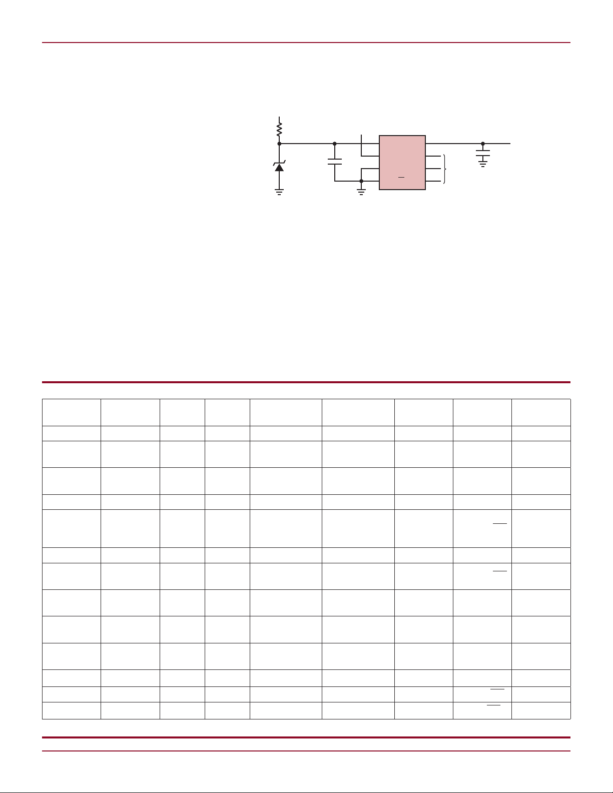
to hold the input voltage at a point
midway between the adjacent cells.
Some type of open wire detection or
cell resistance measuring function
is necessary. The LTC6802 includes
100µA current sources to load the cell
inputs. The current source will cause
large changes in cell readings if there
is an open circuit in the harness.
Figure 10. Cell measurement filtering
5
L DESIGN FEATURES
MUX
C4
C3
C
F4
C
F3
C2
C1
V
–
100µA
B4
B3
LTC6802-1
LTC6802
BATTERY
MONITOR
12 Li-Ion
SERIES
BATTERIES
BATTERY MODULE 8
CAN
TRANSCEIVER
SPI
µCONTROLLER
GALVANIC
ISOLATOR
TO VEHICLE
CAN BUS
CONTROL MODULE
CAN
LTC6802
BATTERY
MONITOR
DIGITAL
ISOLATOR
DIGITAL
ISOLATOR
12 Li-Ion
SERIES
BATTERIES
BATTERY MODULE 1
The host controller must be able
to run diagnostics on all the modules
during normal operation to detect IC
failures. If these periodic self-tests fail,
then the control algorithm is suspect
and the battery pack must be taken off
line. The LTC6802 includes a built-in
self-test in combination with external
support circuits to allow the BMS to
completely verify the data acquisition
system. See the LTC6802 data sheets
for more details.
The LTC6802 Isolates
Communications from
Swings in Ground Potential
Breaking a ~100 cell pack into modules makes it easier to integrate the
analog circuits. Unfortunately, we are
left with the task of getting the data
from measurement IC to the host controller when the difference in ground
potential exceeds 300V. The LTC6802
can solve this problem in a number of
ways, depending on the specific needs
of the application.
The LTC6802 comes in two flavors,
depending on the desired data communication scheme. The LTC6802-1
offers a built-in stackable serial
peripheral interface (SPI) solution
designed for easy daisy chaining of the
interface. The addressable LTC6802-2
is designed for bus-oriented (parallel)
SPI communication, but it can also be
used in a parallel-addressable, daisy
chained interface for a robust and rela-
Figure 11. Current sources help detect open circuits.
tively inexpensive solution. All three
schemes are described below.
SPI Bus Communication with
the Addressable LTC6802-2
and Digital Isolators
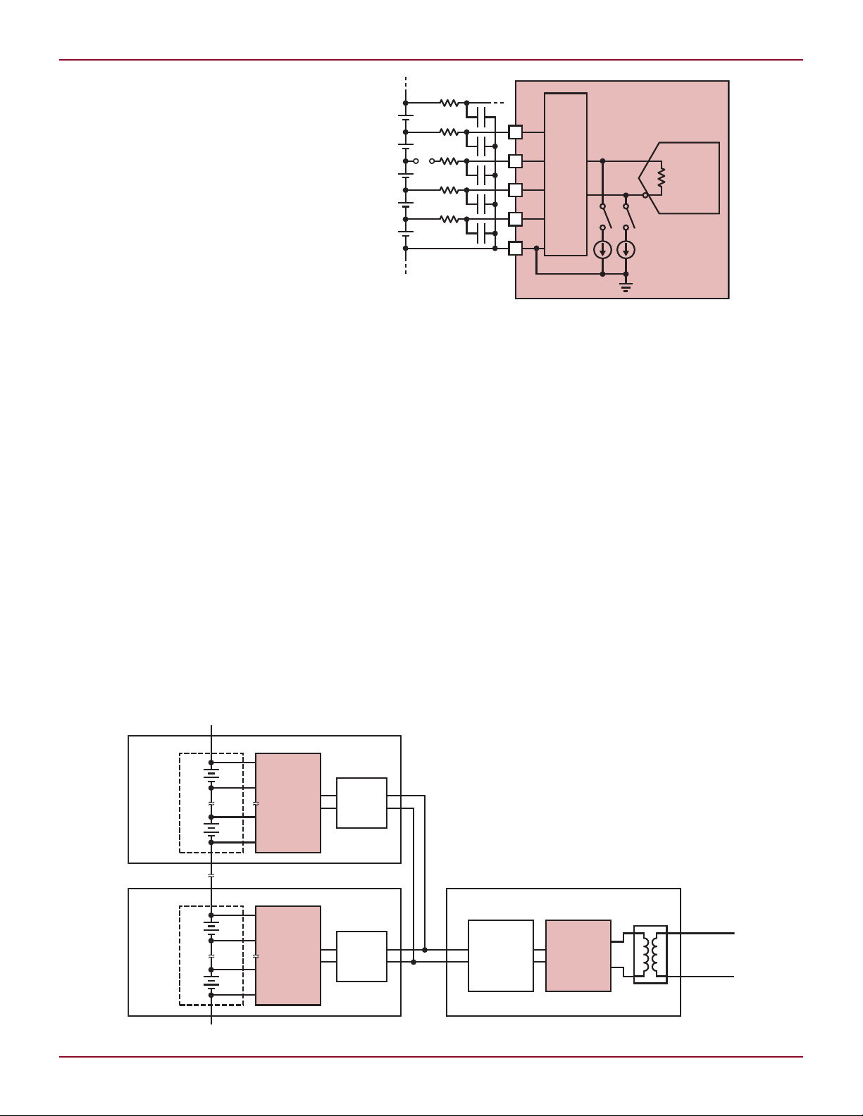
The most straightforward approach is
to use a bus communications scheme,
with a digital isolator between each
module and the host controller. Figure 12 shows a 96-cell pack using
eight multicell modules monitored
by the LTC6802. The physical layer
is a 4-wire SPI bus. An addressing
scheme allows the control module to
talk to the battery modules separately
or in unison. The data buses on the
modules are isolated from one another.
This is a robust scheme, but it has
one major drawback: digital isolators
are expensive and require an isolated
power supply so that the battery cells
don’t have to provide the power to the
cell side of the isolator.
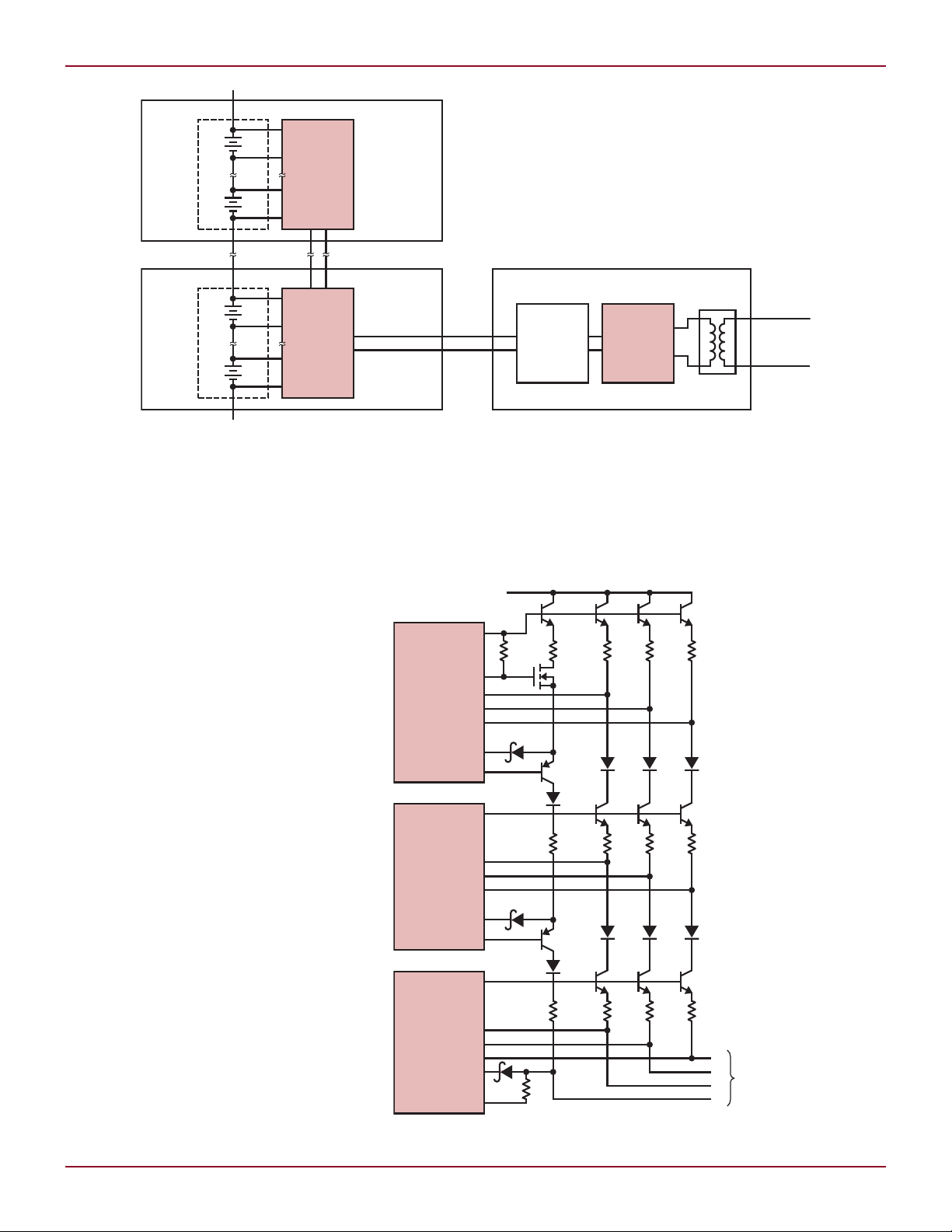
Daisy Chaining the SPI Interface
with the LTC6802-1
The LTC6802-1 provides fixed 1mA
signaling between stacked devices to
enable easy implementation a daisy
chained SPI interface with inexpensive
support circuitry. The digital isolators
are eliminated as shown in Figure 13.
The interface exploits the fact that the
positive supply of module “N” is the
same voltage as the ground of module
“N+1.” A 1mA current is used to transmit data between adjacent modules.
Like the analog circuits, the modular
approach means the data bus has to
deal with a fraction of the total pack
voltage.
6
Figure 12. Using digital isolators to communicate to the LTC6802
Linear Technology Magazine • March 2009
DESIGN FEATURES L
LTC6802
BATTERY
MONITOR
12 Li-Ion
SERIES
BATTERIES
BATTERY MODULE 8
CAN
TRANSCEIVER
SPI
µCONTROLLER
GALVANIC
ISOLATOR
TO VEHICLE
CAN BUS
CONTROL MODULE
CAN
LTC6802
BATTERY
MONITOR
12 Li-Ion
SERIES
BATTERIES
BATTERY MODULE 1
2.2k2.2k1.8k1M
NDC7002N
2.2k
LTC6802-2
IC #3
V
REG
V
BATT
WDT
SDI
SCKI
CSBI
SDO
V
−
2.2k2.2k100Ω
100Ω
2.2k
LTC6802-2
IC #2
V
REG
SDI
SCKI
CSBI
SDO
V
−
2.2k2.2k
R12
2.2k
2.2k
LTC6802-2
IC #1
V
REG
SDI
SCKI
CSBI
SDO
CS
CK
DI
DO
HOST µP
500kbps MAX DATA RATE
ALL NPN: CMPT8099
ALL PNP: CMPT8599
ALL PN: RS07J
ALL SCHOTTKY: CMD5H2-3
V
−
Figure 13. Using the daisy chained SPI to eliminate digital isolators
The disadvantage of any pure daisy
chain is that a fault in one module
results in a loss of communications
with all the modules above it in the
stack. Also, since there is no galvanic
isolation between modules, the interface needs to handle large voltages
that occur during fault conditions.
For example if the “service switch” in
Figure 1 is open and there is a load
on the pack then the data bus connection between modules 4 and 5 will
see a reverse voltage equal to the total
pack voltage (–300V to –400V). The
LTC6802 interface relies on external
discrete diodes to block the reverse
voltage during fault conditions.
The Best of Both Worlds:
Daisy Chained, Addressable
Interface with the LTC6802-2
With inexpensive external circuitry,
the LTC6802-2 can also be used in
a stacked SPI configuration like the
LTC6802-1, but with more flexibility
in the operating parameters.
The SPI port of the LTC6802-2 is
a 4-wire connection: chip select in
(CSBI), clock in (SCKI), data in (SDI),
and data out (SDO). The inputs are
conventional CMOS levels and the
output is an open-drain NMOS. The
SDO pin must have an external pull-up
current or added resistance suitable
for the intended data rate. The IC also
provides a versatile always-on 5V output (V
REG
Linear Technology Magazine • March 2009
), which can produce up to
4mA to energize low power auxiliary
circuitry.
Figure 14 shows a complete stacked
LTC6802-2 SPI interface for a 36cell application. The stack can be
increased in size by replicating the
Figure 14. Inexpensive SPI daisy chain for parallel-addressed LTC6802-2
circuit of the middle IC. In Figure 14,
the V
REG
and V
–
pins of each stacked
IC are used to bias common-base
connected transistors to form a signal
translation current for each SPI data
line. Each LTC6802 can monitor up
7

L DESIGN FEATURES
to 12 cell-potentials, which could sum
to 60V in certain instances, so the
transistors selected for the SPI translation need to have a V
over 60V, but
CBO
they should be the highest available fT
to prevent undue slowing of the logic
signals. A suitable NPN candidate is
the CMPT8099, while the CMPT8599
is its PNP complement, both from
Central Semiconductor. These are fast
80V devices (fT > 150MHz).
Sending Signals Upwards
At the bottom-of-stack IC, the logic
signal is furnished by the host connection, be it a microprocessor or an
SPI isolation device. By simply pulling
down the emitter leg of an NPN having
a V
base potential through a known
REG
resistance, a specific current is formed
for a logic low input signal. In the case
of the component values shown, the
current is about 2mA for a logic low,
and conversely, the transistor is essentially turned off with a logic high
(~0mA for 5V logic).
Since the collector current is nearly
identical to the emitter current, the
same current pulls on the next higher
cascode circuit. Since that next circuit
is the same as the first, the voltage on
the upper emitter resistor reproduces
that of the bottom circuit logic level for
the upper IC. This continues up the
daisy chain, eventually terminating at
the top potential of the battery stack.
Since each IC is provided the same input waveforms, this structure forms a
parallel bus from a logical perspective,
even though each IC is operating at a
different potential in the stack.
The NPN transistors at the top IC
source the logic current directly from
the battery stack. Only small base
currents flow from any V
output.
REG
The 600V collector diodes provide reverse-voltage protection in the event a
battery group interconnection is lost,
perhaps during service (these are not
required for functionality and could
be omitted in some situations).
Bringing Data Down the Stack
The SDO cascode chain is similar in
concept, except the current starts at
the top of the stack and flows downward. At the top IC, a PNP transistor
with its base connected to the local
–
V
pin has current injected into its
emitter by a pullup resistor. Here
again, the collector current is essentially identical to the emitter current,
and so current flows downward
through each successive PNP and terminates into a resistor at the bottom
of stack. In this case, the presence of
the current in the termination resistor,
about 2mA for the component values
shown, forms a logic high potential
for the host interface.
A Schottky diode is connected from
each SDO pin to the emitter of a local
PNP thereby allowing any LTC6802
on the stack to divert the pullup current to the local V
–
when outputting
a logic low. This effectively turns off
the emitter current to the local PNP
transistor and all points lower in the
stack, so the voltage on the bottom
termination resistor then drops to a
logic low level. Since each SDO pin
can force a low level, this forms a
wire-OR function that is equivalent
to paralleled connections as far as
the host interface is concerned. Note
the bottom of stack SDO diode is connected slightly differently; it forms a
direct wire-OR at the host interface.
Since the LTC6802-2 is designed to
use addressed readback commands,
this line is properly multiplexed and
no inter-IC contention occurs.
To eliminate the pull-up current
during standby, a general purpose
N-channel MOSFET is used to interrupt the top PNP emitter current when
the watchdog timer bit goes low. The
watchdog timeout will release when
clock activity is present, so the SDO
line will reactivate as needed. Here
again, an NPN is used at the top of
stack to ensure the pull-up current
comes directly from the battery, rather
than loading V
REG
.
Collector diodes are added here as
well to provide a high reverse voltage
protection capability, plus some added
series resistance is included to protect
the lower transistor emitters from
transient energy (once again, these
protection parts don’t add any other
functionality to the data transmission and could be omitted in some
circumstances).
External SPI Advantages
Since the LTC6802-2 uses a parallel
addressable SPI protocol, the conventional method of connecting multiple
devices in a stack is to provide isolation
for each SPI connection, then parallel
the signals on the host side. Isolators
are relatively expensive and often need
extra power circuitry, thus adding significantly to the total solution cost. The
transistor circuitry shown here is quite
inexpensive and offers the option to
make certain design tradeoffs as well.
With the propagation delays involved
and desire to keep power fairly low, this
circuit as shown still communicates
at over 500kbps. Lower SPI currents
could be chosen in applications that
don’t demand the high data rate by
simply raising the resistance values
accordingly.
The main feature of the transistorized SPI bus is the wide compliance
range that is afforded by the unconstrained collector -base operating
range of the transistors. In normal
operation the VCB ranges from just
less than the cells connected to the
LTC6802, to some five volts below that,
depending on the logic level transmitted. This becomes important since
voltage fluctuations on the battery,
due to load dynamics or switching
transients, affect the VCB of the transistors even though the V+ and ADC cell
inputs may be filtered. Some vehicle
manufacturers are requiring that a
BMS tolerate 1V steps with 200ns
rise/fall time per cell in the stack, so
this is a 12V waveform edge as seen by
the transistors in a typical application.
With the low collector capacitance and
2mA logic level of the transistor chain,
SPI transmissions remain error free
with even this high level of noise.
Conclusion
EVs and HEVs are here to stay. Inherently safe lithium batteries, which
combine energy density, power density, and cycle life, will continue to
evolve to improve the performance of
these vehicles. Battery management
systems using the LTC6802 extract
the most driving distance and lifetime
from the battery pack while lowering
system cost.
L
8
Linear Technology Magazine • March 2009
DESIGN FEATURES L
GND
0
V
OUT
100V/DIV
I
IN(AVG)
2A/DIV
20ms/DIV
VIN = 24V
C
OUT
= 100µF
2V/DIV
250ns/DIV
GND
CHARGE
CLAMP
V
CC
DONE
FAULT
UVLO1
OVLO1
UVLO2
OVLO2
RDCM
RV
OUT
HVGATE
LVGATE
CSP
CSN
FB
RV
TRANS
T1*
1:10
D1
V
OUT
50V TO 450V
V
TRANS
10V TO 24V
V
CC
TO µP
V
CC
LT3751
GND RBG
R6
40.2k
OFF ON
C3
680µF
C2
2.2µF
s5
C1
10µF
•
•
R7
18.2k
R8
40.2k
M1
R5
6mΩ
1W
D2
+
+
C4
100µF
R9
V
TRANS
R1,
154k
R2, 475k
DANGER HIGH VOLTAGE! OPERATION BY HIGH VOLTAGE TRAINED PERSONNEL ONLY
C5
0.47µF
ALL RESISTORS ARE 0805,
1% RESISTORS UNLESS
OTHERWISE NOTED
D1,D2: VISHAY MURS260
M1: IRF3710Z
T1: WURTH 750310349
LIMIT OUTPUT POWER TO
40W FOR 65°C T1 MAX
AMBIENT OPERATION
*
4.7nF
Y RATED
DC/DC Converter, Capacitor Charger
Takes Inputs from 4.75V to 400V
Introduction
High voltage power supplies and capacitor chargers are readily found in
a number of applications, including
professional photoflashes, security
control systems, pulsed radar systems,
satellite communication systems, and
explosive detonators. The LT3751
makes it possible for a designer to
meet the demanding requirements
of these applications, including high
reliability, relatively low cost, safe
operation, minimal board space and
high performance.
The LT3751 is a general purpose
flyback controller that can be used as
either a voltage regulator or as a capacitor charger. The LT3751 operates in
boundary-mode, between continuous
conduction mode and discontinuous
conduction mode. Boundary-mode
operation allows for a relatively small
transformer and an overall reduced
PCB footprint. Boundary-mode also
reduces large signal stability issues
that could arise from using voltagemode or PWM techniques. Regulation
is achieved with a new dual, overlapping modulation technique using both
by Robert Milliken and Peter Liu
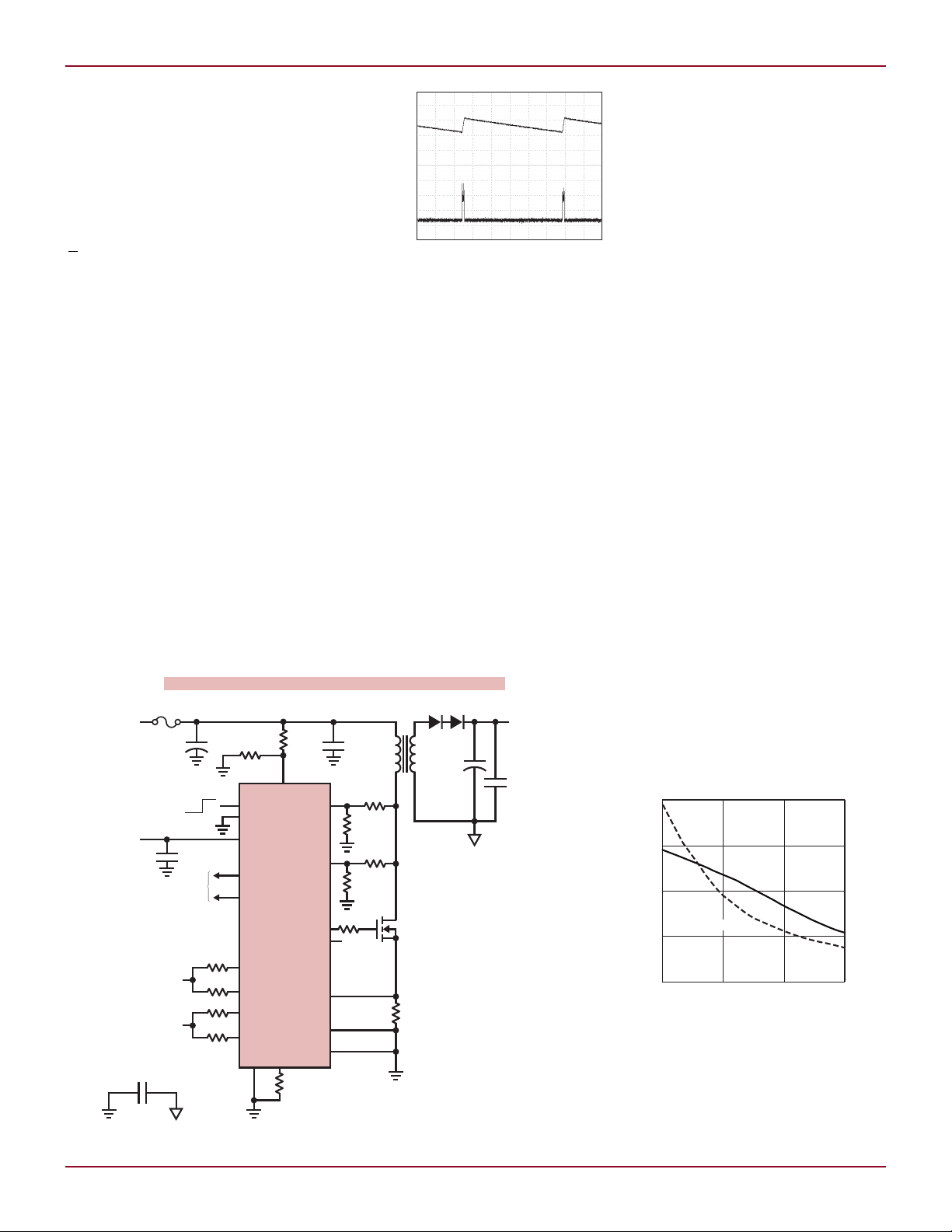
Figure 1. Gate driver waveform
in a typical application
peak primary current modulation and
duty-cycle modulation, drastically reducing audible transformer noise.
The LT3751 features many safety
and reliability functions, including
two sets of undervoltage lockouts
(UVLO), two sets of overvoltage
lockouts (OVLO), no-load operation,
over-temperature lockout (OTLO), internal Zener clamps on all high voltage
pins, and a selectable 5.6V or 10.5V
internal gate driver voltage clamp (no
external components needed). The
LT3751 also adds a start-up/shortcircuit protection circuit to protect
against transformer or external FET
damage. When used as a regulator, the
LT3751’s feedback loop is internally
compensated to ensure stability. The
LT3751 is available in two packages,
either a 20-pin exposed pad QFN or a
20-lead exposed pad TSSOP.
New Gate Driver with Internal
Clamp Requires No External
Components
There are four main concerns when
using a gate driver: output current
drive capability, peak output voltage,
power consumption and propagation
delay. The LT3751 is equipped with a
1.5A push-pull main driver, enough to
drive +80nC gates. An auxiliary 0.5A
PMOS pull-up only driver is also integrated into the LT3751 and is used in
parallel with the main driver for VCC
voltages of 8V and below. This PMOS
driver allows for rail-to-rail operation.
Above 8V, the PMOS driver must be
deactivated by tying its drain to VCC.
Most discrete FETs have a VGS limit
of 20V. Driving the FET higher than
20V could cause a short in the internal gate oxide, causing permanent
Figure 2. Isolated high voltage capacitor charger from 10V to 24V input
Linear Technology Magazine • March 2009
Figure 3. Isolated high voltage capacitor
charger charging waveform
9
L DESIGN FEATURES
R
N
V V
R
OUT TRIP DIODE
9 8
0 98
=
•
+
•
.
( )
0
GND
V
DRAIN
20V/DIV
I
PRIMARY
5A/DIV
10µs/DIV
V
OUT
(V)
EFFICIENCY (%)
LOAD CURRENT (mA)
1000
90
60
20 40 60 80
65
70
80
75
85
402
399
400
401
LOAD REGULATION
EFFICIENCY
0
GND
V
DRAIN
20V/DIV
I
PRIMARY
5A/DIV
10µs/DIV
CHARGE
CLAMP
V
CC
DONE
FAULT
UVLO1
OVLO1
UVLO2
OVLO2
RDCM
RV
OUT
HVGATE
LVGATE
CSP
CSN
FB
RV
TRANS
T1**
1:10
D1
V
OUT
400V
V
TRANS
10V TO 24V
V
CC
TO µP
V
CC
LT3751
GND RBG
R6
40.2k
OFF ON
C3
680µF
R10*
499k
R11
1.54k
C2
2.2µF
s5
C1
10µF
•
•
R7
18.2k
R8
40.2k
M1
R5
6mΩ
1W
D2
+
+
C4
100µF
R9
787Ω
V
TRANS
R1,154k
R2, 475k
DANGER HIGH VOLTAGE! OPERATION BY HIGH VOLTAGE TRAINED PERSONNEL ONLY
C5
0.47µF
C6
10nF
ALL RESISTORS ARE 0805,
1% RESISTORS UNLESS
OTHERWISE NOTED
C4: CDE 380LX101M500J042
C5: TDK CKG57NX7R2J474M
D1,D2: VISHAY MURS260
M1: IRF3710Z
T1: WURTH 750310349
USE TWO SERIES 1206,
1% RESISTORS FOR R10
R10: 249k s2
LIMIT OUTPUT POWER TO
40W FOR 65°C T1 MAX
AMBIENT OPERATION
*
**
Figure 4. A 10V to 24V input, 400V regulated power supply
damage. To alleviate this issue, the
LT3751 has an internal, selectable
5.6V or 10.5V gate driver clamp. No
external components are needed, not
even a capacitor. Simply tie the CLAMP
pin to ground for 10.5V operation or
tie to VCC for 5.6V operation. Figure
1 shows the gate driver clamping at
10.5V with a VCC voltage of 24V.
Not only does the internal clamp
protect the FET from damage, it also
reduces the amount of energy injected
into the gate. This increases overall
efficiency and reduces power consumption in the gate driver circuit. The
gate driver overshoot is very minimal,
as seen in Figure 1. Placing the external
FET closer to the LT3751 HVGATE pin
reduces overshoot.
a. Switching waveform for I
10
High Voltage, Isolated
Capacitor Charger from
10V to 24V Input
The LT3751 can be configured as
a fully isolated stand-alone capacitor charger using a new differential
discontinuo us-conductio n-mode
(DCM) comparator—used to sense
the boundary-mode condition—and
a new differential output voltage
(V
) comparator. The differential
OUT
operation of the DCM comparator and
V
comparator allow the LT3751 to
OUT
accurately operate from high voltage
input supplies of greater than 400V.
Likewise, the LT3751’s DCM comparator and V
input supplies down to 4.75V. This
accommodates an unmatched range
of power sources.
= 100mA b. Switching waveform for I
OUT
Figure 5. High voltage regulator performance
OUT
comparator can work with
= 10mA c. Efficiency and load regulation
OUT
Figure 2 shows a high voltage capacitor charger driven from an input
supply ranging from 10V to 24V. Only
five resistors are needed to operate
the LT3751 as a capacitor charger.
The output voltage trip point can be
continuously adjusted from 50V to
450V by adjusting R9 given by:
The LT3751 stops charging the
output capacitor once the programmed
output voltage trip point (V
OUT(TRIP)
) is
reached. The charge cycle is repeated
by toggling the CHARGE pin. The
maximum charge/discharge rate in
Linear Technology Magazine • March 2009
DESIGN FEATURES L
P
C FREQUENCY
V V V
AVG
OUT
OUT TRIP RIPPLE
=
••
•
1
2
2
( )
–
RRIPPLE
W240
(
)
≤
V
CC
R3, 154k
R4, 475k
CHARGE
CLAMP
V
CC
DONE
FAULT
UVLO1
OVLO1
UVLO2
OVLO2
RV
OUT
HVGATE
LVGATE
CSP
CSN
FB
RV
TRANS
T1***
1:3
D1
V
OUT
500V
V
TRANS
100V TO 400V DC
V
CC
10V TO 24V
TO µP
V
CC
LT3751
GND RBG
R6*
625k
OFF ON
C3
100µF
450V
C2
2.2µF
630V
s5
C1
10µF
•
•
R8
137k ×3
R7
88.7k + 7.5k
R10*
208k
R13,20Ω
M1
FQB4N80
R12
68mΩ
1/4W
D2
+
+
C4
220µF
550V
R5
1.11k
V
TRANS
R1**
1.5M
R2**, 9M
DANGER HIGH VOLTAGE! OPERATION BY HIGH VOLTAGE TRAINED PERSONNEL ONLY
C5
0.47µF
630V
RDCM
F1, 1A
R9
66.5k
R11
14.7k +
17.4k
ALL RESISTORS ARE 0805,
1% RESISTORS UNLESS
OTHERWISE NOTED
C4: HITACHI PS22L221MSBPF
C5: TDK CKG57NX7R2J474M
T1: COILCRAFT HA4060-AL
D1,D2: VISHAY US1M
F1: BUSSMANN PCB-1-R
* USE THREE SERIES 1206, 0.1%
RESISTORS FOR R6 & R10
R6: 249k ×2 + 127k
R10: 66.5k ×2 + 75k
** USE TWO SERIES 1206, 1%
RESISTORS FOR R1 & R2
R1: 750k ×2
R2: 4.53M ×2
*** OUTPUT POWER LIMITED TO
20W FOR 65°C T1 AMBIENT
OPERATION
4.7nF
Y RATED
0
V
OUT
AC RIPPLE
10V/DIV
I
IN(AVG)
20mA/DIV
2s/DIV
CHARGE TIME (ms)
V
OUT,TRIP
(V)
INPUT VOLTAGE (V)
400100
530
490
200 300
500
520
510
1000
400
850
550
700
V
OUT,TRIP
CHARGE TIME
the output capacitor is limited by the
temperature rise in the transformer.
Limiting the transformer surface temperature in Figure 2 to 65°C with no
air flow requires the average output
power to be ≤40W given by:
where V
voltage, V
OUT(TRIP)
is the output trip
is the ripple voltage
RIPPLE
on the output node, and frequency is
the charge/discharge frequency. Two
techniques are used to increase the
available output power: increase the
airflow across the transformer, or increase the size of the transformer itself.
Figure 3 shows the charging waveform
and average input current for a 100µF
output capacitor charged to 400V in
less than 100ms (R
= 976Ω).
9
For output voltages higher than
450V, the transformer in Figure 2 must
be replaced with one having higher
primary inductance and a higher
turns ratio. Consult the LT3751 data
Figure 6. The LT3751 protecting the
output during a no-load condition
sheet for proper transformer design
procedures.
High Voltage Regulated Power
Supply from 10V to 24V Input
The LT3751 can also be used to convert
a low voltage supply to a much higher
voltage. Placing a resistor divider from
the output node to the FB pin and
ground causes the LT3751 to operate as a voltage regulator. Figure 4
shows a 400V regulated power supply
operating from an input supply range
of 10V to 24V.
The LT3751 uses a regulation control scheme that drastically reduces
audible noise in the transformer and
the input and output ceramic bulk
capacitors. This is achieved by using
an internal 26kHz clock to synchronize
the primary winding switch cycles.
Within the clock period, the LT3751
modulates both the peak primary
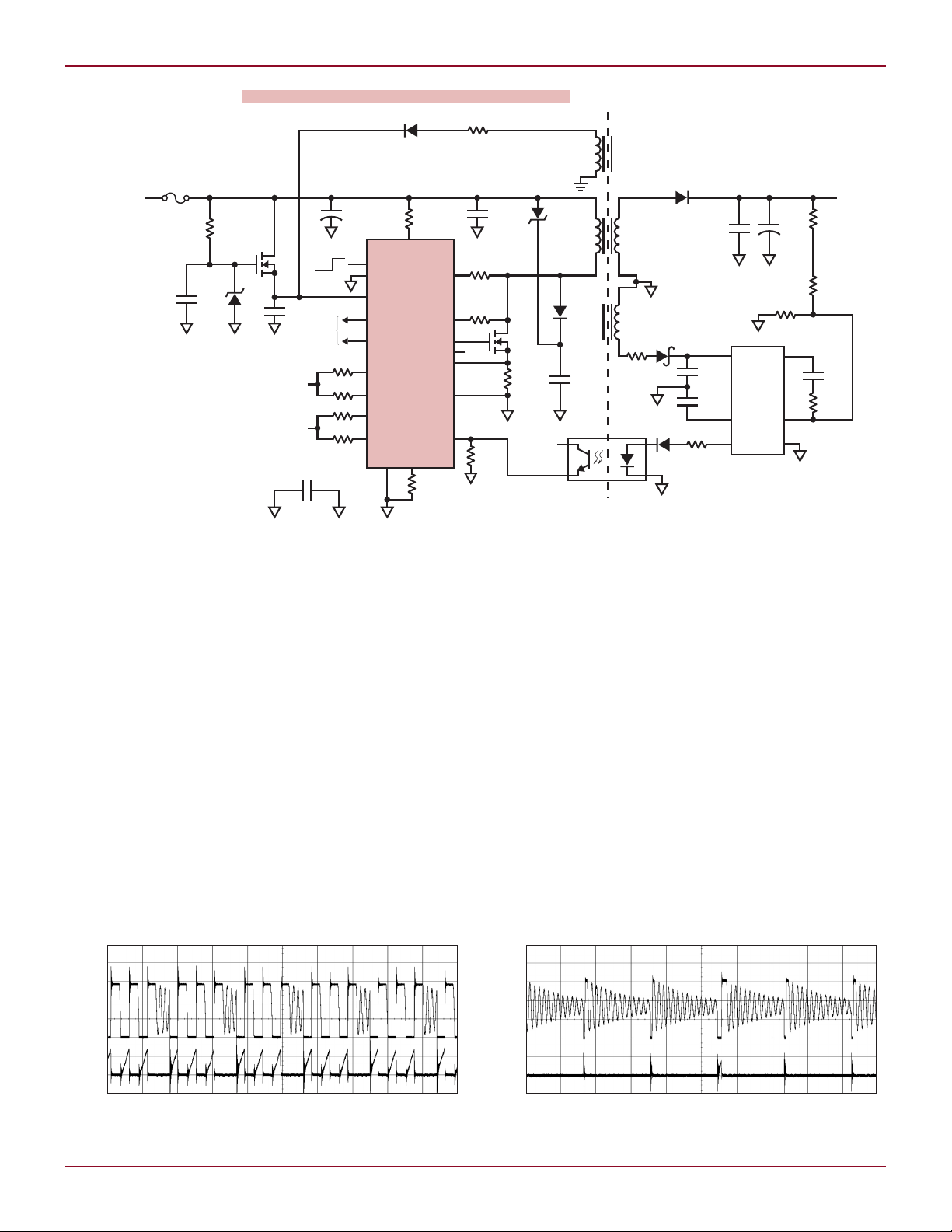
current and the number of switching cycles. Figures 5a and 5b show
heavy-load and light-load waveforms,
respectively, while Figure 5c shows
efficiency over most of the operating
range for the application in Figure 4.
The clock forces at least one switch
cycle every period which would overcharge the output capacitor during a
no-load condition. The LT3751 handles no-load conditions and protects
against over-charging the output node.
Figure 6 shows the LT3751 protecting
during a no-load condition.
Resistors can be added to RV
OUT
and
RBG to add a second layer of protection, or they can be omitted to reduce
component count by tying RV
OUT
and
RBG to ground. The trip level for the
V
comparator is typically set 20%
OUT
higher than the nominal regulation
voltage. If the resistor divider were to
fail, the V
comparator would disable
OUT
switching when the output climbed to
20% above nominal.
Linear Technology Magazine • March 2009
Figure 7. A 100V to 400V input, 500V output, isolated capacitor charger
Figure 8. Isolated capacitor charger V
and charge time with respect to input voltage
OUT(TRIP)
11
L DESIGN FEATURES
OUTPUT VOLTAGE (V)
INPUT VOLTAGE (V)
400100
398
395
200 300
396
397
I
OUT
= 10mA
I
OUT
= 25mA
I
OUT
= 50mA
EFFICIENCY (%)
OUTPUT CURRENT (mA)
750
90
40
50
25 50
60
70
80
VIN = 100V
VIN = 250V
VIN = 400V
V
CC
R3, 154k
R4, 475k
CHARGE
CLAMP
V
CC
DONE
FAULT
UVLO1
OVLO1
UVLO2
OVLO2
RV
OUT
HVGATE
LVGATE
CSP
CSN
FB
RV
TRANS
T1***
1:3
D1
V
OUT
400V
V
TRANS
100V TO 400V DC
V
CC
10V TO 24V
TO µP
V
CC
LT3751
GND RBG
R6*
615k
OFF ON
C3
100µF
C2
2.2µF
s5
C1
10µF
C6
10nF
•
•
R8*
411k
R13,20Ω
M1
FQB4N80
R10
68mΩ
¼W
D2
+
+
C4
100µF
R12
1.54k
R11**
499k
V
TRANS
R1**, 1.5M
R2**, 9M
DANGER HIGH VOLTAGE! OPERATION BY HIGH VOLTAGE TRAINED PERSONNEL ONLY
C5
0.47µF
RDCM
F1, 1A
R9
66.5k
ALL RESISTORS ARE 0805,
1% RESISTORS UNLESS
OTHERWISE NOTED
C4: CDE 380LX101M500J042
C5: TDK CKG57NX7R2J474M
T1: COILCRAFT HA4060-AL
D1,D2: VISHAY US1M
F1: BUSSMANN PCB-1-R
* USE THREE SERIES 1206, 1%
RESISTORS FOR R6 & R8
R6: 205k ×3
R8: 137k ×3
** USE TWO SERIES 1206, 1%
RESISTORS FOR R1, R2 & R11
R1: 750k ×2
R2: 4.53M ×2
R11: 249k ×2
*** OUTPUT POWER LIMITED TO
20W FOR 65°C T1 AMBIENT
OPERATION
R7
95.3k
can also be used for a capacitor
charger. The LT3751 operates as a
capacitor charger until the FB pin
reaches 1.225V, after which the
LT3751 operates as a voltage regulator.
This keeps the capacitor topped-off
until the application needs to use its
energy. The output resistor divider
forms a leakage path from the output
capacitor to ground. When the output
voltage droops, the LT3751 feedback
circuit will keep the capacitor topped-
12
Figure 9. A 100V to 400V input, 400V output, capacitor charger and voltage regulator
Note that the FB pin of the LT3751
a. Overall efficiency b. Line regulation
Figure 10. High voltage input and output regulator performance
off with small, low current bursts of
charge as shown in Figure 6.
High Input Supply Voltage,
Isolated Capacitor Charger
As mentioned above, the LT3751 differential DCM and V
allow the part to accurately work from
very high input supply voltages. An
offline capacitor charger, shown in
Figure 7, can operate with DC input
voltages from 100V to 400V. The transformer provides galvanic isolation from
comparators
OUT
the input supply to output node—no
additional magnetics required.
Input voltages greater than 80V
require the use of resistor dividers
on the DCM and V
comparators
OUT
(charger mode only). The accuracy of
the V
trip threshold is heightened
OUT
by increasing current IQ through R10
and R11; however, the ratio of R6/R7
should closely match R10/R11 with
tolerances approaching 0.1%. A trick
is to use resistor arrays to yield the
desired ratio. Achieving 0.1% ratio accuracy is not difficult and can reduce
the overall cost compared to using
individual 0.1% surface mount resistors. Note that the absolute value of
the individual resistors is not critical,
only the ratio of R6/R7 and R10/R11.
The DCM comparator is less critical
and can tolerate resistance variations
greater than 1%.
The 100V to 400VDC input capacitor charger has an overall V
accuracy of better than 6% over the
entire operating range using 0.1% resistor dividers. Figure 8 shows a typical
performance for V
OUT(TRIP)
and charge
time for the circuit in Figure 7.
Linear Technology Magazine • March 2009
OUT(TRIP)
DESIGN FEATURES L
V
TRANS
100V TO 200V DC
V
CC
V
CC
R11, 84.5k
R12, 442k
UVLO1
OVLO1
UVLO2
OVLO2
DONE
FAULT
CHARGE
CLAMP
V
CC
HVGATE
LVGATE
CSP
CSN
FB
RV
TRANS
TO µP
V
CC
LT3751
LT4430
GND RBG
R3
210k
OFF ON
C3
22µF
350V
s2
C2
1µF
C1
100pF
C4
1µF
250V
s2
C7
400µF
330V
C8
22nF
R17
3.16k
R14
249k
V
OUT
282V
225mA
C6
0.1µF
630V
ISOLATION
BOUNDARY
C5
0.01µF
630V
C9
3.3µF
C10
0.47µF
•
M2
M1
D1
R8
2.49k
R7
475Ω
R18
274Ω
R6
40mΩ
1/4W
V
TRANS
R9, 2.7M
R5, 210k
R13
5.11Ω
R16, 1k
R10, 4.3M
DANGER HIGH VOLTAGE! OPERATION BY HIGH VOLTAGE TRAINED PERSONNEL ONLY
RDCM
RV
OUT
U1
ALL RESISTORS ARE 0805,1% RESISTORS
UNLESS OTHERWISE NOTED
C7: 330FK400M22X38
D1: 12V ZENER
D2: MURS140
D3: P6kE200A
D4, D5: STTH112A
D6: BAT54
D7: BAS516
M1: IRF830
M2: STB11NM60FD
T1: TDK SRW24LQ-UxxH015
(Np:Ns:Npb:Nsb=1:2:0.08:0.08)
U1: PS2801-1
U2: LT4430
R4, 105k
R2, 10ΩD2
D3
D5
D6
D4
Np
Ns
Nsb
U2
VINCOMP
GND
OC FB
OPTO
Npb
T1
D7
R15
221k
R1
49.9k
1/2W
•
•
•
+
+
1
1 1 1
1
11
1
1
1
2
2
2
2
2
2
2
F1, 2A
1 2
4.7nF
Y RATED
0
GND
V
DRAIN
100V/DIV
I
PRIMARY
2A/DIV
20µs/DIV
0
GND
V
DRAIN
100V/DIV
I
PRIMARY
2A/DIV
20µs/DIV
R
V
A
OUT TRIP
11
1 225
50
=
−
( )
.
µ
Figure 11. Fully isolated, high output voltage regulator
High Input Supply Voltage,
Non-Isolated Capacitor
Charger/Regulator
The FB pin of the LT3751 can also
be configured for charging a capacitor from a high input supply voltage.
Simply tie a resistor divider from the
output node to the FB pin. The resistor dividers on the R
pins can tolerate 5% resistors, and all
the R
removed. This lowers the number and
and RBG pin resistors are
V(OUT)
the tolerance of required components,
reducing board real estate and overall
design costs. With the output voltage
resistor divider, the circuit in Figure
9 is also a fully functional, high-efficiency voltage regulator with load
Linear Technology Magazine • March 2009
VTRANS
a. I
and R
= 225mA b. I
OUT
DCM
and line regulation better than 1%.
Efficiency and line regulation for the
circuit in Figure 9 are shown in Figure
10a and Figure 10b, respectively.
Alternatively, a resistor can be tied
from V
pin. This mimics the V
to the OVLO1 pin or OVLO2
OUT
compara-
OUT
tor, stopping charging once the target
voltage is reached. The FB pin is tied
to ground. The CHARGE pin must be
toggled to initiate another charge sequence, thus the LT3751 operates as
a capacitor charger only. Resistor R12
is omitted from Figure 9 and resistor
R11 is tied from V
or OVLO2. R11 is calculated using the
following equation:
Figure 12. Switching waveforms
OUT
directly to OVLO1
Note that OVLO1 or OVLO2 will
cause the FAULT pin to indicate a
fault when the target outpaut voltage,
V
OUT(TRIP) ,
is reached.
High Voltage Input/Output
Regulator with Isolation
Using a resistor divider from the output
node to the FB pin allows regulation
but does not provide galvanic isolation.
Two auxiliary windings are added to
the transformer in circuit shown in
Figure 11 to drive the FB pin, the
OUT
= 7.1mA
continued on page 42
13
L DESIGN FEATURES
V
REF
+IN
–IN
GND
8
7
6
5
1
2
3
4
V
CC
CLK
D
OUT
CS/SHDN
LTC1286
V
IN
5V
0.1µF
5V
18k
LT1634-4.096
µC/µP
SERIAL
INTERFACE
0.1µF
How to Choose a Voltage Reference
by Brendan Whelan
Why Voltage References?
It is an analog world. All electronic
devices must in some way interact with
the “real” world, whether they are in
an automobile, microwave oven or cell
phone. To do that, electronics must be
able to map real world measurements
(speed, pressure, length, temperature)
to a measurable quantity in the electronics world (voltage). Of course, to
measure voltage, you need a standard
to measure against. That standard is
a voltage reference. The question for
any system designer is not whether he
needs a voltage reference, but rather,
which one?
A voltage reference is simply that—a
circuit or circuit element that provides
a known potential for as long as the circuit requires it. This may be minutes,
hours or years. If a product requires
information about the world, such
as battery voltage or current, power
consumption, signal size or characteristics, or fault identification, then the
signal in question must be compared
to a standard. Each comparator, ADC,
DAC, or detection circuit must have a
voltage reference in order to do its job
(Figure 1). By comparing the signal of
interest to a known value, any signal
may be quantified accurately.
Figure 1. Typical use of a voltage reference for an ADC
Reference Specifications
Voltage references come in many forms
and offer different features, but in
the end, accuracy and stability are
a voltage reference’s most important
features, as the main purpose of the
reference is to provide a known output
voltage. Variation from this known
value is an error. Voltage reference
specifications usually predict the
uncertainty of the reference under
Table 1. Specifications for high performance voltage references
Temperature
Coefficient
Initial
Accuracy
I
S
Architecture V
OUT
Voltage
Noise*
Long-Term
Drift
Package
LT1031 5ppm/°C 0.05% 1.2mA Buried Zener 10V 0.6ppm 15ppm/kHr H
LT1019 5ppm/°C 0.05% 650µA Bandgap
LT1027 5ppm/°C 0.05% 2.2mA Buried Zener 5V 0.6ppm
2.5V, 4.5V,
5V, 10V
2.5ppm SO-8, PDIP
20ppm/
month
SO-8, PDIP
LT1021 5ppm/°C 0.05% 800µA Buried Zener 5V, 7V, 10V 0.6ppm 15ppm/kHr SO-8, PDIP, H
1.25V, 2.048V,
LTC6652 5ppm/°C 0.05% 350µA Bandgap
2.5V, 3V, 3.3V,
2.1ppm 60ppm/√kHr
MSOP
4.096V, 5V
LT1236 5ppm/°C 0.05% 800µA Buried Zener 5V, 10V 0.6ppm 20ppm/kHr SO-8, PDIP
LT1461 3ppm/°C 0.04% 35µA Bandgap
LT1009 15ppm/°C 0.2% 1.2mA Bandgap 2.5V 20ppm/kHr
LT1389 20ppm/°C 0.05% 700nA Bandgap
LT1634 10ppm/°C 0.05% 7µA Bandgap
2.5V, 3V, 3.3V,
4.096V, 5V
1.25V, 2.5V,
4.096V, 5V
1.25V, 2.5V,
4.096V, 5V
8ppm 60ppm/√kHr
MSOP-8,
SO-8, Z
20ppm SO-8
6ppm
SO-8,
MSOP-8, Z
LT1029 20ppm/°C 0.20% 700µA Bandgap 5V 20ppm/kHr Z
LM399 1ppm/°C 2% 15mA Buried Zener 7V 1ppm 8ppm/√kHr
LTZ1000 0.05ppm/°C 4% Buried Zener 7.2V 0.17ppm 2µV/√kHr H
*0.1Hz–10Hz, Peak-to-Peak
14
Linear Technology Magazine • March 2009
SO-8
H

DESIGN FEATURES L
TEMPERATURE (˚C)
–50
OUTPUT VOLTAGE (NORMALIZED) (V)
1.001
1.002
1.003
25 75
1.000
0.999
–25 0
50 100 125
0.998
0.997
5ppm/oC
0oC TO 70oC “BOX”
LT1019
CURVE
UNCOMPENSATED
“STANDARD” BANDGAP
DRIFT CURVE
10ppm/oC
FULL TEMP RANGE “BOX”
certain conditions using the following
definitions.
Initial Accuracy
The variance of output voltage as
measured at a given temperature,
usually 25°C. While the initial output
voltage may vary from unit to unit, if
it is constant for a given unit, then it
can be easily calibrated.
Temperature Drift
This specification is the most widely
used to evaluate voltage reference
performance, as it shows the change
in output voltage over temperature.
Temperature drift is caused by imperfections and nonlinearities in the
circuit elements, and is often nonlinear
as a result.
For many parts, the temperature
drift, TC, specified in ppm/°C, is the
dominant error source. For parts with
consistent drift, calibration is possible.
A common misconception regarding
temperature drift is that it is linear.
This leads to assumptions such as
“the part will drift a lesser amount
over a smaller temperature range.”
Often the opposite is true. TC is generally specified with a “box method” in
order to give an understanding of the
likely error over the entire operating
temperature range. It is a calculated
value based only on minimum and
maximum values of voltage, and does
not take into account the temperatures
at which these extrema occur.
For voltage references that are very
linear over the specified temperature
range, or for those that are not carefully tuned, the worst-case error can
be assumed to be proportional to the
temperature range. This is because
the maximum and minimum output
voltages are very likely to be found at
the maximum and minimum operating
temperatures. However, for very carefully tuned references, often identified
by their very low temperature drift,
the nonlinear nature of the reference
may dominate.
fied as 100ppm/°C tends to appear
quite linear over any temperature
For example, a reference speci-
range, as the drift due to component
mismatches completely obscures the
Linear Technology Magazine • March 2009
Figure 2. Voltage reference
temperature characteristics
inherent nonlinearity. In contrast, the
temperature drift of a reference specified as 5ppm/°C will be dominated by
the nonlinearities.
Voltage references come
in many forms and offer
different features, but in the
end, accuracy and stability
are a voltage reference’s
most important features,
as the main purpose of
the reference is to provide
a known output voltage.
Variation from this known
value is an error. Voltage
reference specifications
usually predict the
uncertainty of the reference
under certain conditions.
This can be easily seen in the output
voltage vs temperature characteristic
of Figure 2. Note that there are two
possible temperature characteristics
represented. An uncompensated
bandgap appears as a parabola, with
minima at the temperature extrema
and maximum in the middle. A
temperature compensated bandgap,
such as the LT1019, shown here,
appears as an “S” shaped curve, with
greatest slope near the center of the
temperature range. In the latter case,
nonlinearity is exacerbated so that the
aggregate uncertainty over temperature is reduced.
The best use of the temperature drift
specification is to calculate maximum
total error over the specified temperature range. It is generally inadvisable
to calculate errors over unspecified
temperature ranges unless the temperature drift characteristics are well
understood.
Long Term Stability
This is a measure of the tendency of a
reference voltage to change over time,
independent of other variables. Initial
shifts are largely caused by changes
in mechanical stress, usually from the
difference in expansion rates of the
lead frame, die and mold compound.
This stress effect tends to have a large
initial shift that reduces quickly with
time. Initial drift also includes changes
in electrical characteristics of the
circuit elements, including settling
of device characteristics at the atomic
level. Longer-term shifts are caused
by electrical changes in the circuit
elements, often referred to as “aging.”
This drift tends to occur at a reduced
rate as compared to initial drift, and to
further reduce over time. It is therefore
often specified as drift/
khr. Voltage
√
references tend to age more quickly
at higher temperatures.
Thermal Hysteresis
This often-overlooked specification
can also be a dominant source of error. It is mechanical in nature, and is
the result of changing die stress due
to thermal cycling. Hysteresis can be
observed as a change in output voltage
at a given temperature after a large
temperature cycle. It is independent
of temperature coefficient and time
drift, and reduces the effectiveness
of initial voltage calibration.
Most references tend to vary around
a nominal output voltage during
subsequent temperature cycles, so
thermal hysteresis is usually limited
to a predictable maximum value. Each
manufacturer has their own method
for specifying this parameter, so typical
values can be misleading. Distribution
data, as provided in data sheets such
as the LT1790 and LTC6652, is far
more useful when estimating output
voltage error.
15

L DESIGN FEATURES
5V
4.7M
LT1389-1.25
V
OUT
1.25V
0.1MF
2.6V b VINb 18V
1MF
V
OUT
= 2.5V
LT1790-2.5
82.4k135k
14.9k2.8k
2.5k
Q1
Q2
2k
Q1
Q5
20pF
20pF
7.5k
5007500k
60k
300k
50k
200k
V
REF
1.235V, 0mV/°C
240mV, +0.8mV/°C
60mV, +0.2mV/°C
360mV, +1.2mV/°C
575mV, –2.2mV/°C
600k
Q3
Q11
Q10
Q9
Q14
–
+
–
–
–
+
+
+
Q8
Q6
Q4
Q12
Q13
Figure 3. Shunt voltage reference
Other Specifications
Additional specifications that may be
important, depending on application
requirements include:
q
Voltage Noise
q
Line Regulation/PSRR
q
Load Regulation
q
Dropout Voltage
q
Supply Range
q
Supply Current
Reference Types
The two main types of voltage reference
are shunt and series. See Table 2 for
a list of Linear Technology series and
shunt voltage references.
Shunt References
The shunt reference is a 2-terminal
type, usually designed to work over a
specified range of currents. Though
most shunts are of the bandgap type
and come in a variety of voltages, they
can be thought of and are as simple
to use as a Zener diode.
The most common circuit ties one
terminal of the reference to ground and
the other terminal to a resistor. The
remaining terminal of the resistor is
Figure 4. Series voltage reference
then tied to a supply. This becomes, in
essence, a three terminal circuit. The
shared reference/resistor terminal
is the output. The resistor must be
chosen such that the minimum and
maximum currents through the reference are within the specified range
over the entire supply range and load
current range. These references are
quite easy to design with, provided
the supply voltage and load current do
not vary much. If either, or both, may
change substantially, then the resistor must be chosen to accommodate
this variance, often forcing the circuit
to dissipate significantly more power
than required for the nominal case. It
can be considered to function like a
class A amplifier, in that sense.
Advantages of shunt references
include simple design, small packages
and good stability over wide current
and load conditions. In addition, they
are easily designed as negative voltage
references and can be used with very
high supply voltages, as the external
resistor holds off most of the potential,
or very low supplies, as the output can
be as little as a few millivolts below
the supply. Linear Technology offers
shunt products including the LT1004,
LT1009, LT1389, LT1634, LM399 and
LTZ1000. A typical shunt circuit can
be seen in Figure 3.
Series References
Series references are three (or more)
terminal devices. They are more like
low dropout (LDO) regulators, so they
have many of the same advantages.
Most notably, they consume a relatively fixed amount of supply current over
a wide range of supply voltages, and
they only conduct load current when
the load demands it. This makes them
ideal for circuits with large changes in
supply voltage or load current. They
are especially useful in circuits with
very large load currents as there is no
series resistor between the reference
and supply.
Series products available from Linear Technology include the LT1460,
LT1790, LT1461, LT1021, LT1236,
LT1027, LTC6652, LT6660, and many
others. Products such as the LT1021
and LT1019 may be operated either as
a shunt or a series voltage reference.
A series reference circuit is illustrated
in Figure 4.
Figure 5. A bandgap circuit is designed for a theoretically zero temperature coefficient.
16
Figure 6. A 200mV reference circuit
Linear Technology Magazine • March 2009

DESIGN FEATURES L
Reference Circuits
There are many ways to design a voltage reference IC. Each has specific
advantages and disadvantages.
Zener-Based References
The buried Zener type reference is a
relatively simple design. A Zener (or
avalanche) diode has a predictable
reverse voltage that is fairly constant
over temperature and very constant
over time. These diodes are often very
low noise and very stable over time if
held within a small temperature range,
making them useful in applications
where changes in the reference voltage
must be as small as possible.
This stability can be attributed to
the relatively small number of components and die area as compared
to other types of reference circuits,
as well as the careful construction
of the Zener element. However, relatively high variances in initial voltage
and temperature drift are common.
Additional circuitry may be added to
compensate these imperfections, or
to provide a range of output voltages.
Both shunt and series references use
Zener diodes.
Devices like the LT1021, LT1236
and LT1027 use internal current
sources and amplifiers to regulate the
Zener voltage and current to increase
stability, as well as to provide various
output voltages such as 5V, 7V and
10V. This additional circuitry makes
the Zener diode more compatible with
a wide variety of application circuits,
but requires some additional supply
headroom and may cause additional
error.
Alternatively, the LM399 and
LTZ1000 use internal heating elements and additional transistors to
stabilize the temperature drift of the
Zener diode, giving the best combination of temperature and time stability.
In addition, these Zener-based products have extraordinarily low noise,
giving the best possible performance.
The LTZ1000 exhibits 0.05ppm/°C
temperature drift, 2µV/√kHr long
term stability and 1.2µV
give some perspective, in a laboratory
instrument, the total uncertainty in
the LTZ1000’s reference voltage due
noise. To
P-P
Table 2. Voltage references available from Linear Technology
Type Part Description
LT1019 Precision Bandgap
LT1021 Precision Low Noise Buried Zener
LT1027 Precision 5V Buried Zener
LT1031 Precision Low Noise/Low Drift 10V Zener
LT1236 Precision Low Noise Buried Zener
LT1258 Micropower LDO Bandgap
Series
Shunt
LT1460 Micropower Precision Bandgap
LT1461 Micropower Ultra-Precision Bandgap
LT1790 Micropower Low Dropout Bandgap
LT1798 Micropower LDO Bandgap
LT6650 Micropower 400mV/Adjustable Bandgap
LTC6652 Precision Low Noise LDO Bandgap
LM129 Precision 6.9V Buried Zener
LM185 Micropower 1.2V/2.5V Zener
LM399 Precision 7V Heated Zener
LT1004 Micropower 1.2V/2.5V Bandgap
LT1009 Precision 2.5V Bandgap
LT1029 5V Bandgap
LT1034 Micropower Dual (1.2V Bandgap/7V Zener)
LT1389 Nanopower Precision Bandgap
LT1634 Micropower Precision Bandgap
LTZ1000 Ultra-Precision Heated Zener
to noise and temperature would be
only about 1.7ppm plus a fraction of
1ppm per month due to aging.
transistors. Figure 5 shows a simplified version of the LT1004 circuit, a
basic bandgap. It can be shown that
a mismatched pair of bipolar junction
Bandgap References
While Zener diodes can be used to
make very high performance references, they lack flexibility. Specifically,
they require supply voltages above 7V
and they offer relatively few output
voltages. In contrast, bandgap references can produce a wide variety
of output voltages with little supply
headroom—often less than 100mV.
Bandgap references can be designed
to provide very precise initial output
voltages and low temperature drift,
eliminating the need for time-consuming in-application calibration.
Bandgap operation is based on a
basic characteristic of bipolar junction
transistors has a difference in VBE
that is proportional to temperature.
This difference can be used to create
a current that rises linearly with temperature. When this current is driven
through a resistor and a transistor, the
change over temperature of the baseemitter voltage of the transistor cancels
the change in the voltage across the
resistor if it is sized properly. While
this cancellation is not completely
linear, it can be compensated with
additional circuitry to yield very low
temperature drift.
The math behind the basic bandgap
voltage reference is interesting in that
it combines known temperature coef-
Linear Technology Magazine • March 2009
17

L DESIGN FEATURES
ΔV
kT
q
AREA Q
AREA Q
BE
=•
ln
10
11
–
+
–
+
COMP B
COMP A
400mV
REFERENCE
OUTB
V
S
–INB
+INA
OUTA
GND
V
S
LT6700-1
LT6700HV-1
–
+
–
+
COMP B
1M
COMP A
ALKALINE
AA CELLS
VR = 400mV
REFERENCE
1M
0.1µF
LT6700-3
63.4k
261k
1M
V
BATT
> 1.6V
V
BATT
> 2V
MONITOR CONSUMES ~10µA
HYSTERESIS IS APPROXIMATELY
2% OF TRIP VOLTAGE
V
BATT
1.4V (MIN)
3V (NOM)
+
+
V
S
ficients with unique resistor ratios to
produce a voltage reference with theoretically zero temperature drift. Figure
5 shows two transistors scaled so that
the emitter area of Q10 is 10-times that
of Q11, while Q12 and Q13 hold their
collector currents equal. This creates
a known voltage between the bases of
the two transistors of:
where k is the Boltzmann constant in
J/kelvin (1.38 × 10
-23
), T is tempera-
ture in kelvin (273 + T(°C)) and q is
the charge of an electron in coulombs
(1.6x10
-19
). At 25°C, kT/q has a value
of 25.7mV with a positive temperature
coefficient of 86µV/°C. ΔV
BE
voltage times ln(10), or 2.3, for a 25°C
voltage of approximately 60mV with a
tempco of 0.2mV/°C.
Applying this voltage to the 50k
resistor tied between the bases creates
a current that is proportional to temperature. This current biases a diode,
Q14 with a 25°C voltage of 575mV with
a –2.2mV/°C temperature coefficient.
Resistors are used to create voltage
drops with positive tempcos, which
are added to the Q14 diode voltage,
thus producing a reference voltage
potential of approximately 1.235V
with theoretically 0mV/°C tempera-
ture coefficient. These voltage drops
are shown in Figure 5. The balance of
the circuit provides bias currents and
output drive.
Linear Technology produces a
wide variety of bandgap references,
including the LT1460, a small and
inexpensive precision series reference, the LT1389, an ultralow power
shunt reference, and the LT1461 and
LTC6652, which are very high precision, low drift references. Available
output voltages include 1.2V, 1.25V,
2.048V, 2.5V, 3.0V, 3.3V, 4.096V,
4.5V, 5V and 10V. These reference
voltages can be provided over a wide
range of supplies and load conditions
with minimal voltage and current overhead. Products may be very precise,
as with the LT1461, LT1019, LTC6652
and LT1790; very small, as with the
LT1790 and LT1460 (SOT23), or
18
is this
Figure 7. The LT6700 allows comparisons
with thresholds as low as 400mV.
LT6660 in a 2mm × 2mm DFN package; or very low power, such as the
LT1389, which requires only 800nA.
While Zener references often have
better performance in terms of noise
and long term stability, new bandgap
references such as the LTC6652, with
2ppm peak-to-peak noise (0.1Hz to
10Hz) are narrowing the gap.
Fractional Bandgap References
These are references based on the
temperature characteristics of bipolar
transistors, but with output voltages
that may be as low as a few millivolts.
They are useful for very low voltage
circuits, especially in comparator applications where the threshold must
Figure 8. Higher thresholds are set by dividing the input voltage.
be less than a conventional bandgap
voltage (approximately 1.2V).
Figure 6 shows the core circuit from
the LM10, which combines elements
that are proportional and inversely
proportional to temperature in a
similar fashion to the normal bandgap
reference to obtain a constant 200mV
reference. A fractional bandgap usu-
ally uses a ΔV
to generate a current
BE
that is proportional to temperature,
and a VBE to generate a current that
is inversely proportional. These are
combined in the proper ratio in a
resistor element to generate a temperature-invariant voltage. The size
of the resistor may be varied to alter
the reference voltage without affecting
the temperature characteristic. This
differs from a traditional bandgap
circuit in that the fractional bandgap
circuit combines currents, while the
traditional circuits tend to combine
voltages, usually a base-emitter voltage and an I•R with opposite TC.
Fractional bandgaps like the LM10
circuit are based in part on a subtraction as well. The LT6650 has a 400mV
reference of this type, combined with
an amplifier. This allows the reference voltage to be altered by changing
the gain of the amplifier, and gives a
buffered output. Any output voltage
from 0.4V to a few millivolts below
the supply voltage can be generated
with this simple circuit. In a more
integrated solution, the LT6700
(Figure 7) and LT6703 combine a
Linear Technology Magazine • March 2009

DESIGN FEATURES L
400mV reference with comparators,
and can be used as voltage monitors
or window comparators. The 400mV
reference allows monitoring of small
input signals, which decreases the
complexity of monitor circuits and
enables monitoring of circuit elements
working on very low supplies as well.
For larger thresholds, a simple resistor
divider may be added (Figure 8). Each
of these products is available in a small
footprint package (SOT23), consumes
low power (less than 10µA) and works
on a wide supply range (1.4V to 18V).
In addition, the LT6700 is available in
a 2mm × 3mm DFN package and the
LT6703 is available in a 2mm × 2mm
DFN package.
Choosing a Reference
So, now, with all those options, how do
you choose the right reference for your
application? Here are a few hints that
can narrow the range of options:
q
Is the supply voltage very
high? Choose a shunt.
q
Does the supply voltage or
load current vary widely?
Choose a series.
q
Require high power efficiency?
Choose a series.
q
Figure your real-world
temperature range. Linear
Technology provides guaranteed
specifications and operation
over various temperature ranges
including 0°C to 70°C, –40°C to
85°C and –40°C to 125°C.
q
Be realistic about required
accuracy. It is important to
understand the precision required
by the application. This will help
identify critical specifications.
With the requirement in mind,
multiply temperature drift by the
specified temperature range. Add
initial accuracy error, thermal
hysteresis, and long term drift
over the intended product life.
Remove any terms that will be
factory calibrated or periodically
recalibrated. This gives an
idea of total accuracy. For the
most demanding applications,
noise, line regulation and load
regulation errors may also
be added. As an example, a
reference with 0.1% (1000ppm)
initial accuracy error, 25ppm/°C
temperature drift over –40°C
to 85°C, 200ppm thermal
hysteresis, 2ppm peak-to-peak
noise and 50ppm/√kHr time drift
would have a total uncertainty
of over 4300ppm at the time the
circuit is built. This uncertainty
increases by 50ppm in the
first 1000 hours the circuit is
powered. The initial accuracy
may be calibrated, reducing the
error to 3300ppm + 50ppm •
(t/1000hours)
√
.
Linear Technology offers
a wide variety of voltage
reference products. These
include both series and
shunt references—using
Zeners, bandgaps and
other schemes. References
are available in multiple
performance and
temperature grades, as
well as in nearly every
conceivable package type.
q
What is the real supply range?
What is the maximum expected
supply voltage? Will there be
fault conditions such as battery
load dump or hot-swap inductive
supply spikes that the reference
IC must withstand? This may
significantly reduce the number
of viable choices.
q
How much power can the
reference consume? References
tend to fall into a few categories:
more than 1mA, ~500µA,
<300µA, <50µA, <10µA, <1µA.
q
How much load current?
Will the load draw substantial
current or produce current that
the reference must sink? Many
references can provide only small
currents to the load and few can
absorb substantial current. The
load regulation specification is a
good guide.
q
How much room do you have?
References come in a wide
variety of packages, including
metal cans, plastic packages
(DIP, SOIC, SOT) and very small
packages, including the LT6660
in a 2mm × 2mm DFN. There is a
widely held view that references
in larger package sizes have less
error due to mechanical stress
than smaller packages. While
it is true that some references
may give better performance in
larger packages, there is evidence
that suggests performance
difference has little to do directly
with the package size. It is more
likely that because smaller dice
are used for products that are
offered in smaller packages, some
performance tradeoffs must be
made to fit the circuit on the die.
Usually, the package’s mounting
method makes a more significant
performance difference than
the actual package—careful
attention to mounting methods
and locations can maximize
performance. Also, devices with
smaller footprints can show
reduced stress when a PCB bends
compared to devices with larger
footprints. This is discussed in
detail in application note AN82,
“Understanding and Applying
Voltage References,” available
from Linear Technology.
Conclusion
Linear Technology offers a wide variety of voltage reference products.
These include both series and shunt
references designed with Zeners,
bandgaps and other types. References
are available in multiple performance
and temperature grades and nearly
every conceivable package type. Products range from the highest precision
available to small and inexpensive
alternatives. With a vast arsenal of
voltage reference products, Linear
Technology’s voltage references meet
the needs of almost any application.
See also Linear Technology’s application note AN82 “Understanding
and Applying Voltage References,”
available at www.linear.com.
L
Linear Technology Magazine • March 2009
19

L DESIGN FEATURES
V
BUS
OV
SENS
D0–D2
CHRG
NTC
USB
WALL
ADAPTER
HIGH VOLTAGE INPUT
7.5V TO 30V
TRANSIENT
TO 60V
SYSTEM
LOAD
M1
(OPTIONAL)
L1 = TDK, VLCF5020T-4R7NIR7-1
L2 = COILCRAFT, LPS4018-332MLC
M1 = VISHAY, Si 2333DS
D1 = DIODES INC., DFLS240
SEE THE LTC4098 DATASHEET FOR MORE INFORMATION
ON CONFIGURING THE NTC BATTERY TEMPERATURE
QUALIFICATION OR REDUCED IDEAL DIODE IMPEDANCE.
SINGLE-CELL
Li-Ion
C5
0.1µF
L2
3.3µH
L1
4.7µH
LTC4098
GND
SW
V
OUT
BATSENS
PROGCLPROG
WALLV
C
LT3653
HVOK
GNDV
C
I
LIM
R3
1k
R2
3.01k
R4
6.04k
R1
27.4k
C4
10µF
6.3V
D1
TO µC
TO µC
C1
4.7µF
50V
C2
22µF
6.3V
C3
0.1µF
10V
V
IN
V
OUT
I
SENSE
SW
BOOST
OV
GATE
BAT
IDGATE
1.2A Monolithic Buck Regulator
Shrinks Supply Size and Cost with
Programmable Output Current Limit
Introduction
Power supplies are often overqualified
for their job. This is because power
ICs often specify a current limit that
is more than twice the rated output
current of the device. The power supply
components are sized to handle the
maximum current that the IC can deliver, even if loads are unlikely to draw
that current during normal operation.
The components are bigger and more
expensive than they need to be.
set an accurate maximum output cur-
rent on the supply once the real world
load is known. Accurately setting the
maximum output current reduces the
required current rating of the regulator’s power path components, thus
replacing big, expensive components
with smaller, less expensive ones.
A limit on the regulator’s maximum
Figure 1. Charging a single cell Li-ion battery from either a USB input or high voltage input. This
solution offers a seamless, highly efficient, low part count approach to dual input charging and
PowerPath™ control of a Li-ion battery-powered application. If additional integration is required
for more system supplies, the LT3653 can be used in a similar fashion with the LTC3576 PMIC.
20
There is, however, an alternative:
output limits the maximum power
dissipation of both the supply and
the load, thus reducing the potential
for localized heating. Monitoring and
controlling the output current also
makes for a robust solution, which is
able to withstand harsh overload and
short circuit conditions.
The LT3653 and LT3663 are monolithic step-down switching regulators
that have an accurate output current
limit programmable from 400mA to
1.2A. The LT3663 is a general purpose high voltage step-down regulator
while the LT3653 is designed for use
with Linear Technology Bat-Track™
enabled battery chargers and power
management ICs (PMICs). The maximum input voltages of 30V (LT3653)
or 36V (LT3663) with 60V transient
ride through capability are well suited
by Tom Sheehan
to automotive, industrial, distributed
supply, and wall transformer applications.
Programmable
Output Current Limit
Monolithic switching regulators typically limit the peak switch current to
protect the internal switch from being
damaged during an overload or short
circuit event. The maximum switch
peak current limit is typically more
than two times the maximum output
current rating of the part. While the
peak switch current limit prevents
overstressing the IC, it does not keep
the entire application from overheating during an overload condition. For
example, a regulator with an output
current rating of 1A is typically capable
of providing over 2A at the output.
During an output overload condition,
the power dissipation of the regulator could more than double, making
thermal management more difficult.
The LT3653 and LT3663 reduce localized hot spots by controlling the total
power dissipation of the application
with a programmable, accurate current limit.
Conservative design principles call
for power path components that are
rated for worst-case currents. In the
above example, where a 1A part is
capable of delivering 2A, the power
path components must be sized for
greater than 2A, because during an
output short circuit or overload the
inductor and diode can conduct up
to 2A. In contrast, the PowerPath
components in LT3653 and LT3663
applications are sized based on the
programmed maximum output current limit. Therefore, an application
with a 750mA output current limit
requires only 750mA rated components. This allows for smaller, lower
Linear Technology Magazine • March 2009

DESIGN FEATURES L
LT3663
V
IN
V
IN
RUN
I
LIM
BOOST
SW
GND
0.1µF
2.2µF
22µF59k28.7k
11k
6.8µH
DIODES,
INC.
DFLS240
I
SENSE
V
OUT
V
OUT
FB
ON OFF
OUTPUT CURRENT (A)
OUTPUT VOLTAGE (V)
6
5
4
0
1
2
3
0 0.2 0.4 0.6 0.8 1 1.41.2
R
ILIM
= 28.7k
cost devices and a smaller overall
application footprint.
In early product development,
system designers usually don’t know
how much current their load will draw.
Once they choose a power supply, they
are committed. However, with the programmable current limit of the LT3653
and LT3663, once the load has been
fully characterized, they can change
the output current limit by changing
an inexpensive 1% resistor.
The output current limit is implemented by monitoring and controlling
the average inductor current. When an
overcurrent event occurs, the regulator
disables the power switch. This robust
solution withstands short circuit and
overload conditions throughout the
entire input voltage range.
The LT3653 Plays Well with
Bat-Track Battery Chargers
The LT3653 is a 1.5MHz constant
frequency, current mode control,
step-down regulator designed for use
with Linear Technology’s Bat-Track-
enabled battery charger PowerPath
power managers. The LT3653 steps
down a high voltage input to power the
system load and charge a single-cell
Li-ion battery charger.
Minimizing the voltage across
a linear battery charger increases
efficiency. To accomplish this, a BatTrack battery charger controls the
LT3653’s VC Pin, overriding the error
amplifier. In this way, the output voltage of the LT3653 is regulated by the
battery charger to a potential slightly
above the battery voltage, typically
300mV.
Figure 3. A LT3663 application producing
5V at 1.2A from an input of 7.5V to 36V. The
input is capable of handling 60V transients.
Linear Technology Magazine • March 2009
LT3653 programmed current limit, the
regulator’s output voltage decreases to
reduce charge current as the battery
charger enters dropout. If the system
load continues to increase, the battery
charge current first decreases to zero
and then reverses direction to deliver
power to the system load, supplementing the LT3653. The transitions
between these modes of operation are
seamless to the system load. The output current from the LT3653 regulator
Figure 2. The LT3663 output
current limit at 1.2A
Input overvoltage protection allows
the LT3653 to handle 60V input transients. The HVOK pin indicates that
the internal bias supplies are present
and no faults have occurred (i.e., overtemperature and input overvoltage
and undervoltage). The LT3653 includes internal compensation, and
an internal boost diode to minimize
the number of external components.
The LT3653 is available in an 8-lead
2mm × 3mm DFN package with an
exposed pad.
never exceeds the programmed output
current limit.
The LT3663 Directly
Accepts 36V Inputs
The LT3663 is a 1.5MHz constant
frequency, current mode control,
general purpose, monolithic switching regulator suited for automotive
batteries, industrial power supplies, distributed supplies, and wall
transformers. The LT3663 includes
a low current shutdown mode, input
overvoltage and undervoltage lockout,
and thermal shutdown. The LT3663 is
available in 8-lead (2mm × 3mm) DFN
package with exposed pad. An 8-lead
Charging a Single Cell Li-Ion
Battery from Either a USB
or High Voltage Input
Figure 1 shows a LT3653 and LTC4098
application charging a single cell Liion battery from either a USB input
or high voltage input. This solution
offers a seamless, highly efficient, low
part count approach to dual input
charging and power path control of a
Li-ion battery-powered application. If
additional integration is required for
more system supplies, the LT3653 can
be used in a similar fashion with the
LTC3576 PMIC.
When a high voltage input is applied, the LT3653 HVOK pin signals
the LTC4098 that it is capable of
delivering power. The LTC4098 takes
control of the LT3653’s VC pin and
MSOP package with exposed pad will
be available soon.
The LT3663 can also function as
a constant current, constant voltage
(CC/CV) source to charge a supercapacitor or other energy storage device.
The IC operates in constant current
mode at the programmed current
limit until the capacitor reaches the
programmed output voltage. It then
operates in a constant voltage mode
to maintain that voltage.
Figure 2 shows the LT3663 output current limit at 1.2A. For output
currents below 1.2A the regulator is
in constant voltage mode. When the
output current is increased to 1.2A it
goes into constant current mode. The
output current is maintained at 1.2A
from V
nominal down to 0V.
OUT
regulates the output voltage to just
above the battery voltage. This BatTrack function optimizes the battery
charger efficiency.
When present, the high voltage
input supplies the battery charge current and the system load current. If
the total current increases beyond the
7.5V–36V to 5V Buck
Regulator with 1.2A
Output Current Limit
Figure 3 shows a LT3663 application
producing 5V at 1.2A from an input
of 7.5V to 36V. The input is capable
continued on page 29
21

L DESIGN FEATURES
TEMPERATURE (°C)
–40
QUIESCENT CURRENT (µA)
10
6
8
2
4
0
12080400
VCC = 3.6V
OUTPUT VOLTAGE (V)
0
AVERAGE INPUT CURRENT (µA)
1000
100
10
4020 3010
VCC = 3.6V
VCC VOLTAGE (V)
0
QUIESCENT CURRENT (µA)
12
10
6
8
2
4
0
161284
Boost Converters for Keep-Alive
Circuits Draw Only 8.5µA of
Quiescent Current
Introduction
Industrial remote monitoring systems
and keep-alive circuits spend most of
their time idle. Many of these systems
use batteries, so to maximize run time
power losses,even during low power
idle modes, must be minimized. Even
at no load, power supplies draw some
current to produce a regulated voltage
for keep-alive circuits.
The LT8410/-1 DC/DC boost
converter features ultralow quiescent
current and integrated high value
feedback resistors to minimize the
draw on the battery when electronics
are idle.
An entire boost converter takes very
little space, as shown in Figure 1.
Ultralow Quiescent Current
Low Noise Boost Converter
with Output Disconnect
When a micropower boost converter
is in regulation with no load, the
input current depends mainly on
two things—the quiescent current
(required to keep regulation) and the
output feedback resistor value. When
the output voltage is high, the output
feedback resistor can easily dissipate
more power than the quiescent current
of the IC. The quiescent current of the
LT8410/-1 is a low 8.5µA, while the
integrated output feedback resistors
have very high values (12.4M/0.4M).
This enables the LT8410/-1 to dissipate very little power in regulation
at no load. In fact, the LT8410/-1 can
regulate a 16V output at no load from
3.6V input with about 30µA of average
input current. Figures 2, 3 and 4 show
the typical quiescent and input current
in regulation with no load.
The LT8410/-1 controls power
delivery by varying both the peak
inductor current and switch off time.
This control scheme results in low
output voltage ripple as well as high
efficiency over a wide load range. As
shown in Figure 5, even with a small
0.1µF output capacitor, the output
ripple is typically less than 10mV. The
part also features output disconnect,
which disconnects the output voltage
from the input during shutdown. This
output disconnect circuit also sets a
maximum output current limit, allowing the chip survive output shorts.
An Excellent Choice for
High Impedance Batteries
A power source with high internal
impedance, such as a coin cell battery,
may show normal output voltage on
a voltmeter, but its voltage can collapse under heavy current demands.
This makes it incompatible with high
by Xiaohua Su
Figure 1. The LT8410/-1 is designed
to facilitate compact board layout.
switch-current DC/DC converters.
The LT8410/-1 has an integrated
power switch and Schottky diode,
and the switch current limits are very
low (25mA for the LT8410 and 8mA
for the LT8410-1). This low switch
current limit enables the LT8410/-1
to operate very efficiently from high
impedance sources, such as coin cell
batteries, without causing inrush
current problems. Figure 6 shows
the LT8410-1 charging an electrolytic
capacitor. Without any additional external circuitry, the input current for
Figure 2. Quiescent current vs
temperature—not switching
22
Figure 3. Quiescent current
vs VCC voltage—not switching
Figure 4. Average input current
in regulation with no load
Linear Technology Magazine • March 2009

1 30 1
1
2
. •+
R
R
( . ) ( )1 24 3 10 1
1
2
1 10
7 7
−••+
−•
−−
R
R
R
R
SW CAP
GND
CHIP
ENABLE
FBP
LT8410
2.2µF
0.1µF
100µH
0.1µF
0.1µF*
V
OUT
= 16V
V
IN
2.5V to 16V
V
CCVOUT
V
REF
SHDN
604K
412K
*HIGHER VALUE CAPACITOR IS REQUIRED
WHEN THE VIN IS HIGHER THAN 5V
LOAD CURRENT (mA)
0.01
V
OUT
PEAK-TO-PEAK RIPPLE (mV)
10
8
2
6
4
0
1010.1
VIN = 3.6V
LOAD CURRENT (mA)
0.01
EFFICIENCY (%)
100
50
60
70
80
90
40
100100.1 1
VIN = 12V
VIN = 5V
VIN = 3.6V
Figure 5. General purpose bias with wide input voltage and low output voltage ripple
SW CAP
GND
FBP
LT8410-1
C1
2.2µF
C3
10000µF
C4
0.1µF
L1
220µH
C2
1.0µF
V
OUT
= 16V
V
IN
2.5V to 16V
V
CCVOUT
V
REF
SHDN
R1
604k
R2
412k
TURN ON/OFF
C1: 2.2μF, 16V, X5R, 0603
C2: 1.0μF, 25V, X5R, 0603*
C3: 10000μF, Electrolytic Capacitor
C4: 0.1μF, 16V, X7R, 0402
L1: COILCRAFT LPS3008-224ML
* HIGHER CAPACITANCE VALUE IS REQUIRED FOR
C2 WHEN THE VIN IS HIGHER THAN 12V
SHDN VOLTAGE
2V/DIV
V
OUT
VOLTAGE
10V/DIV
INPUT CURRENT
5mA/DIV
INDUCTOR
CURRENT
10mA/DIV
VIN = 3.6V 20s/DIV
R1
R2
R3
CONNECT TO
SHDN PIN
ENABLE VOLTAGE
the entire charging cycle is less than
8mA.
LT8410/-1 to fit almost anywhere.
Figure 1 shows the size of a circuit
similar to that shown in Figure 4,
Tiny Footprint with
Small Ceramic Capacitors
Available in a tiny 8-pin 2mm × 2mm
illustrating how little board space
is required to build a full featured
LT8410/-1 application.
DFN package, the LT8410/-1 is internally compensated and stable for
a wide range of output capacitors. For
most applications, using 0.1µF output
capacitor and 1µF input capacitor is
sufficient. An optional 0.1µF capacitor
at the V
pin implements a soft-start
REF
feature. The combination of small
package size and the ability to use
small ceramic capacitors enable the
SHDN Pin Comparator and
Soft-Start Reset Feature
An internal comparator compares the
SHDN pin voltage to an internal volt-
age reference of 1.3V, giving the part
a precise turn-on voltage level. The
SHDN pin has built-in programmable
hysteresis to reject noise and tolerate
slowly varying input voltages. Driving
DESIGN FEATURES L
the SHDN pin below 0.3V shuts down
the part and reduces input current to
less than 1µA. When the part is on, and
the SHDN pin voltage is close to 1.3V,
0.1µA current flows out of the SHDN
pin. A programmable enable voltage
can be set up by connecting external
resistors as shown in Figure 7.
The turn-on voltage for the con-
figuration is:
and the turn-off voltage is:
where R1, R2 and R3 are resistance
in Ω. Programming the turn-on/turn-
off voltage is particularly useful for
applications where high source impedance power sources are used, such as
energy harvesting applications.
By connecting an external capacitor (typically 47nF to 220nF) to the
V
pin, a soft-start feature can be
REF
implemented. When the part is brought
continued on page 29
Figure 7. Programming the enable
voltage by using external resistors
Linear Technology Magazine • March 2009
Figure 6. Capacitor charger with the LT8410-1 and charging waveforms
23

L DESIGN FEATURES
SWI/O
I/O
RESET
DA
FB
R
T
SYNC
fSW = 700kHz
WDI
RST
WDO
V
IN
µP
EN/UVLO
V
IN
4.5V TO 36V
TRANSIENT TO 60V
3.3V
800mA
100k
C
WDT
10nF
t
WDU
= 182ms
t
WDL
= 5.9ms
12µH
10pF
22µF
0.1µF
MBRM140
316k
GND
21k
LT3689
BST
OUT
C
POR
C
WDT
2.2µF
C
POR
68nF
t
RST
= 157ms
Industrial/Automotive Step-Down
Regulator Accepts 3.6V to 36V
and Includes Power-On Reset and
Watchdog Timer in 3mm × 3mm QFN
Introduction
As the number of microprocessors in
automotive and industrial applications continues to expand, so does the
need for rugged step-down regulators
that can operate over a wide input
voltage range and withstand high
voltage transients and output shorts.
Microprocessor -based applications
also require supervisory functions,
such as power-on reset (POR) and
watchdog timing, to ensure high system reliability. The regulator must
have high efficiency at light loads
to increase battery life. The LT3689
delivers all of these features in tiny
16-pin 3mm × 3mm QFN and 16-pin
MSOP packages.
Features of the LT3689
Step-Down Regulator
The LT3689 employs a constant frequency, current mode architecture to
provide 800mA of continuous output
current. The part operates from a
wide 3.6V to 36V input range and can
protect itself from input transients up
to 60V. It is internally compensated,
which helps to lower the external component count. The switching frequency
can be set anywhere between 350kHz
and 2.2MHz by tying a resistor from
24
Figure 1. LT3689 typical application circuit with reset time
set to 157ms and watchdog timeout period set to 182ms
the RT pin to ground, allowing the designer to optimize component size and
efficiency. The switching frequency can
also be synchronized to an external
clock for noise sensitive applications.
An external resistor divider programs
the output voltage to any value above
the part’s 0.8V reference. Also, the
boost diode is integrated into the IC
to minimize solution size and cost.
Figure 1 shows a typical application
of LT3689.
Soft-Start and Output
Short Circuit Protection
The LT3689 includes a soft-start feature that limits the maximum inrush
current during start-up and recovery
from fault conditions. The soft-start
circuit ramps up the peak switch
current limit in approximately 150µs,
reducing the peak input current.
The DA pin is used to monitor the
current in the catch diode. If the catch
diode current at the end of switch
cycle is higher than the DA current
limit then the part delays the switch
turn-on until the catch diode current
drops below the DA current limit. This
protects the LT3689 in the face of
inductor current runaway situations,
by Ramanjot Singh
especially during output overload or
short at high switching frequencies
with high input voltages and small
inductor values. Other protection
features such as frequency foldback,
cycle-by-cycle current limit, and thermal shutdown together ensure that
the part is not damaged by excessive
switch currents during startup, overload or short circuit.
Pin Selectable Modes of
Operation: Low Ripple
Burst Mode Operation
and Pulse-Skipping Mode
Two modes of operation can be selected
through the SYNC pin. Applying a logic
low to the SYNC pin enables the low
ripple Burst Mode® operation, which
maintains high efficiency at light loads
while keeping output ripple low. In
Burst Mode operation, the LT3689
delivers single cycle bursts of current
to the output capacitor followed by
sleep periods. Between bursts, all circuitry associated with controlling the
output switch is shutdown, reducing
the VIN pin and OUT pin currents in
a typical application to a mere 50µA
and 75µA, respectively. As the load
current decreases to a no load condition, the percentage of sleep time
increases, thus decreasing average
input current.
A logic high on SYNC disables Burst
Mode operation, allowing the part to
skip pulses at light loads. The advantage of this pulse-skipping mode over
Burst Mode operation is that the part
continues to switch at the programmed
frequency (set by RT) down to very low
load currents, above 15mA at 12V
in a typical application.
Linear Technology Magazine • March 2009
IN

DESIGN FEATURES L
POR COMPARATOR OVERDRIVE VOLTAGE AS PERCENTAGE
OF RESET THRESHOLD, V
RST
(%)
0.10
400
TRANSIENT DURATION (µs)
500
600
700
800
1.00 10.00 100.00
300
200
100
0
RESET OCCURS
ABOVE THE CURVE
50ms/DIV
V
OUT
2V/DIV
C
POR
1V/DIV
RST
2V/DIV
t
RST
= 165ms
C
POR
= 71.3nF
Programmable
Undervoltage Lockout
The LT3689 can be shutdown by pulling the EN/UVLO pin below 0.3V. In
shutdown, quiescent current is less
than 0.5µA. The EN/UVLO pin can
also be used to perform an accurate
undervoltage lockout (UVLO) function.
A resistor divider from VIN pin can be
used to program the UVLO threshold
of the circuit using the 1.26V accurate
threshold of the EN/UVLO pin. A 4µA
current hysteresis on this pin is also
provided to allow the user to program
desired voltage hysteresis. The LT3689
also has an internal UVLO that prevents the part from switching if VIN
pin ever goes below 3.3V (typical). The
part only starts switching when VIN is
higher than 3.4V and EN/UVLO pin
is above the 1.26V threshold.
Low Dropout
The LT3689 features low dropout for
output voltages above 3V. The minimum operating voltage of the device
is determined either by the LT3689’s
internal undervoltage lockout or
by its maximum duty cycle. Unlike
many buck regulators, the LT3689
can extend its duty cycle by staying
on for multiple cycles, provided that
the boost capacitor is charged above
the minimum voltage of 2.5V. Eventually, after several switching cycles, the
boost capacitor discharges. Internal
circuitry detects this condition and
charges the boost capacitor only when
needed. Also, a bigger boost capacitor
allows even higher duty cycle, allowing extremely low dropout operation.
The dropout voltage for a 5V typical
application is about 400mV at 200mA
load and 900mV at 800mA load.
Figure 2. Power-on reset feature of LT3689
Linear Technology Magazine • March 2009
Power-On Reset (POR)
Many microprocessor -based applications powered by the output
of a switching regulator must know
when the regulator output is ready
and stable before the microprocessor
starts operating. Likewise, once running, the electronic system must be
warned when the regulator output has
dropped below a minimum tolerable
threshold, such as during overload or
shutdown conditions. This is required
to prevent unreliable operation and to
allow the microprocessor to perform
housekeeping operations before power
is completely lost.
The LT3689’s accurate internal
voltage reference and glitch immune
precision POR comparator and timer
circuit feed these specific needs of
microprocessor-based applications.
The switcher’s output voltage must
be above 90% of programmed value
for its RST pin to remain high (refer
to Figure 2). The LT3689 asserts
RST during power-up, power-down
and brown-out conditions. Once the
output voltage rises above the RST
threshold, the adjustable reset timer
is started and RST is released after the
reset timeout period. On power-down,
once output voltage drops below RST
threshold, RST is held at a logic low.
The reset timer is adjustable using an
external capacitor. The RST pin has a
weak pull up to the OUT pin.
The POR comparator is designed to
avoid false triggering. High frequency
noise on the FB pin can falsely trip
RST, particularly when the monitored
output is already near the reset threshold. This can cause oscillatory behavior
at the RST pin. The traditional way of
tackling this problem is to add some
DC hysteresis in the comparator input,
which changes the threshold point
once the output flips. The problem
is that the addition of DC hysteresis
makes the trip voltage less accurate,
since the trip point changes once the
output changes. The LT3689 does not
use hysteresis. Instead, it performs an
integration-like function on transient
events at the comparator. In this way
the magnitude and duration of the
event are both important to the comparator threshold. Figure 3 illustrates
the typical transient duration versus
comparator overdrive (as a percentage
of trip threshold) required to trip the
comparator.
Selecting the Reset
Timing Capacitor
The reset timeout period is adjustable
in order to accommodate a variety of
microprocessor applications. The reset
timeout period, t
, is adjusted by
RST
connecting a capacitor between the
C
pin and ground. The value of this
POR
capacitor is determined by:
C
= t
POR
with C
• 432 • 10
RST
in Farads and t
POR
onds. The C
–9
in sec-
value per millisecond
POR
RST
of delay can also be expressed as
C
/ms = 432 (pF/ms).
POR
Leaving the C
pin unconnected
POR
generates a minimum reset timeout
of approximately 25µs with 10kΩ
pull-up to 5V on RST pin. Maximum
reset timeout is limited by the largest
available low leakage capacitor. The
accuracy of the timeout period will
be affected by capacitor leakage (the
nominal charging current is 2µA) and
capacitor tolerance. A low leakage ceramic capacitor is recommended.
Watchdog Modes:
Timeout or Window
The LT3689 also includes an adjustable watchdog timer that monitors a
microprocessor’s activity. If a code
execution error occurs in a µP, the
watchdog detects the error and sets
the WDO pin low. This signal can
be used to interrupt a routine or to
reset a µP.
Figure 3. Typical transient duration
vs POR comparator overdrive
25

L DESIGN FEATURES
t
WDU
t
WDU
t < t
WDL
t
RST
t
RST
t
RST
WATCHDOG TIMING (W/T = HIGH), TIMEOUT MODE
WDO
WDI
WDI
WDO
WATCHDOG TIMING (W/T = LOW), WINDOW MODE
t
RST
= PROGRAMMED RESET PERIOD
t
WDU
= WATCHDOG UPPER BOUNDARY PERIOD
t
WDL
= WATCHDOG WINDOW MODE LOWER BOUNDARY PERIOD
VUV = OUTPUT VOLTAGE RESET THRESHOLD
The watchdog is operated either
in timeout or window mode (refer to
Figure 4). In timeout mode, the microprocessor needs to toggle the WDI pin
before the watchdog timer expires to
keep the WDO pin high. If the voltage
on the WDI pin does not transition
during the programmed timeout period
then the circuitry pulls WDO low.
In window mode, the WDI pin’s
negative-going pulses must appear
inside a programmed time window to
prevent WDO from going low. If more
than two falling pulses are registered
in the lower boundary period (t
the WDO pin is forced low. The WDO
pin also goes low if no negative edge
is supplied to the WDI pin within the
upper boundary period (t
During a code execution error, the
microprocessor outputs WDI pulses
that are either too fast or too slow.
This condition asserts WDO low and
forces the microprocessor to reset the
program.
In window mode, the WDI signal is
bounded by an upper and lower boundary periods for normal operation. The
period of the WDI input signal should
be longer than the window mode’s lower boundary period and shorter than
the upper boundary period to keep
WDO high under normal conditions.
The window mode’s lower and upper
boundary periods have a fixed ratio
of 31. These times can be increased
or decreased by adjusting an external
capacitor on the C
In both watchdog modes, when
WDO is asserted, the reset timer is
enabled. Any WDI pulses that appear
while the reset timer is running are
ignored. When the reset timer expires,
the WDO is allowed to go back high
again. Therefore, if no input is applied
to the WDI pin then the watchdog
circuitry produces a train of pulses
on the WDO pin. The high time of
this pulse train is equal to the upper
boundary period and low time is equal
to the reset period. Also, WDO and
RST cannot be logic low simultaneously. If WDO is low and there is an
undervoltage lockout fault, RST goes
low and WDO will go high.
The WDE pin allows the user to turn
on or off the watchdog function. This
26
WDT
pin.
WDU
).
WDL
),
Figure 4. Watchdog timing diagram
feature can be used to reliably program
the connected microprocessor in the
factory. During factory programming
of the microprocessor, WDE pin can
be kept high to prevent WDO from
toggling and thus prevents WDO from
interfering with the microprocessor’s
programming procedure.
Tying the WDO and RST pins
together will generate a reset signal
when either the output voltage falls
10% below the regulation value or if
there is a watchdog error.
Selecting the Watchdog
Timing Capacitor
The watchdog upper boundary period
is adjustable and can be optimized
for software execution. The watchdog
upper boundary period is adjusted by
connecting a capacitor between the
C
pin and ground. Given a specified
WDT
watchdog upper boundary period, the
capacitor is determined by:
C
= t
WDT
• 55 (pF/ms)
WDU
The window mode lower boundary
period has a fixed relationship to upper
boundary period for a given capacitor.
The lower boundary period is related
to the upper boundary period by the
following:
t
= 1/31 • t
WDL
WDU
Leaving the C
pin unconnected
WDT
generates a minimum watchdog upper boundary period of approximately
200µs with 10kΩ pull-up to 5V on
WDO pin. Maximum timeout is limited
by the largest available low leakage
capacitor. The accuracy of the upper
and lower boundary periods is affected
by capacitor leakage (the nominal
charging current is 2µA) and capacitor tolerance. A low leakage ceramic
capacitor is recommended.
Conclusion
The wide input range, low quiescent
current, supervisory features, robustness and small size of the LT3689
makes it an ideal candidate to power
automotive and industrial applications. The part withstands 60V VIN
transients and normal operation is
guaranteed for max VIN of 36V, and
the part is robust against inrush and
short circuit conditions. The Burst
Mode circuitry provides high efficiencies at light loads. Programmable
switching frequency allows the designer to trade off between component
size and efficiency. The accurate POR
and Watchdog circuitry of LT3689
allows complete supervisory control
of a microprocessor connected to
the output of the LT3689 switching
regulator.
L
Linear Technology Magazine • March 2009

DESIGN FEATURES L
I
APD
= 1mA 500ns/DIV
500µV/DIV
C1
1µF
MONIN
V
REF
R
T
SHDN
CTRL
GND
SYNC
V
OUT
FB
V
IN
SW
LT3571
MON APD
OFF ON
V
IN
5V
R2
20.5k
R4
49.9Ω
45V
R
T
12.1k
1MHz
R
SENSE
20Ω
C4
0.1µF
C3
10nF
R3
10k
C5
10nF
L: TDK VLF3010AT – 100MR49
C1: TDK X7R C1608X7R1C105KT
C2, C4: MURATA X7R GRM188R72A104KA35
C3: AVX X7R 06031C103K
C5: MURATA X7R GRM155R71H103K
50V
C2
0.1µF
L1
10µH
R1
1M
Complete APD Bias Solution in 60mm2
with On-the-Fly Adjustable Current
Limit and Adjustable V
Introduction
The overriding factor limiting functionality in fiber-optic communication
systems is available space. A compact
APD (avalanche photo diode) bias
solution with a high degree of feature
integration is the key to breaking
new ground in system size and per formance. The LT3571 offers such a
solution in a tiny 3mm × 3mm QFN
package.
The LT3571 combines a current
mode step-up DC/DC converter and
a high side fixed voltage drop APD
current monitor with an integrated
75V power switch and Schottky diode.
The combination of a traditional voltage loop and a unique current loop
allows customers to set an accurate
APD current limit at any given bias
voltage. The integrated high side current monitor provides an 8% accurate
current that is proportional to the load
current, making it possible to adjust
the APD bias voltage via the CTRL
pin. This feature-rich device makes
it possible to produce a single stage
boost converter to bias high voltage
APDs in only 60mm2.
Low Noise APD Bias Supply
The gain of the APD is dependent on the
bias voltage, so the bias supply must
minimize the noise contamination
from switching regulators and other
sources. Figure 1 shows the LT3571
configured to produce an ultralow
noise power supply for a 45V APD
with 2.5mA of load current capability.
The MONIN voltage is regulated by
the internal voltage reference and the
resistor divider made up of R1 and R2.
Resistor R
APD current limit at 200mV/1.2R
– 0.2mA.
internal reference, making it possible
The CTRL pin can override the
to optimize the APD bias on the fly
to maximize receiver performance.
SENSE
is selected to set the
SENSE
When the CTRL pin is connected to a
supply above 1V, the output voltage is
regulated with feedback at 1V. When
driven below 1V, the feedback and the
output voltage follow accordingly.
The APD pin, the output of the current monitor, provides a voltage to the
APD load that is fixed 5V below the
MONIN pin. The LT3571 includes a
precise current mirror with a factorof-five attenuation. The proportional
current output signal at the MON pin
can be used to accurately indicate the
Figure 2. The LT3571 evaluation board
APD
Figure 1. Low noise APD bias supply
By Xin (Shin) Qi
APD signal strength. The voltage variance of APD pin voltage is only ±200mV
over the entire input current range and
the whole temperature range. Figure
2 shows the evaluation board for this
topology.
The topology uses several filter
capacitors to achieve ultralow noise
performance. The capacitor at V
pin and the 0.1µF capacitor at the
APD pin suppress switching noise. The
10nF feedforward capacitor across the
MONIN and FB pins filters out high
frequency internal reference and error
amplifier noise. Figure 3 shows the
measured switching noise is less than
500µV
at 1mA load current. This
P–P
exceptionally low noise bias voltage
Figure 3. AC-coupled noise ripple at APD pin
OUT
Linear Technology Magazine • March 2009
27

L DESIGN FEATURES
C1
1µF
MONIN
V
REF
R
T
SHDN
CTRL
GND
SYNC
V
OUT
FB
V
IN
SW
LT3571
MON APD
OFF ON
V
IN
5V
R2
15k
R4
49.9Ω
50V
R
T
33.2k
400kHz
R
SENSE
49.9Ω
C4
0.1µF
C3
10nF
R3
10k
C5
10nF
Q1
L1: TDK VLF4012AT – 150MR63
C1: TDK X7R C1608X7R1C105KT
C2: MURATA X7R GRM21AR72A224KAC5L
C3: AVX X7R 06031C103K
C4: MURATA X7R GRM188R72A104KA35
C5: MURATA X7R GRM155R71H103K
C6: MURATA X7R GRM155R71A104KA01D
55V
C2
0.22µF
L1
15µH
R1
1M
R7
49.9k
R5
30.1k
R6
100k
R9
20kC60.1µF
R8
36.5k
Q2
TEMPERATURE
COMPENSATION BLOCK
Q1, Q2 = PHILIPS PEMT1
50ns/DIV
PWM GND
PWM
1V/DIV
OUT
500mV/DIV
TRD< 100ns
I
APD
= 1mA
I
APD
= 10µA
OUT GND
50ns/DIV
PWM GND
PWM
1V/DIV
OUT
500mV/DIV
TFD< 100ns
I
APD
= 10µA
I
APD
= 1mA
OUT GND
C1
1µF
MONIN
V
REF
R
T
SHDN
CTRL
GND
SYNC
V
OUT
FB
V
IN
SW
LT3571
MON APD
OFF ON
V
IN
3.3V
R2
18.2k
50V
R
T
26.1k
500kHz
L1: TDK VLF3010AT-100MR49
C1: MURATA X7R GRM21BR71C105KA01B
C2, C3: MURATA X7R GRM188R72A104KA35
R
SENSE
20Ω
55V
2.5V
C2
0.1µF
C3
0.1µF
L1
10µH
R1
1M
+
–
PMBT3904
0.5pF
4.99k
4.99k
0.1µF
LT1815
APD PIN
PWM
1k
–V
LO
–V
HI
MEASURE
HERE
FOR TEST PURPOSES,
REPLACE APD WITH
THIS SIMPLE TEST SETUP
gives the APD greater sensitivity and
dynamic range.
Fast APD Current Monitor
Transient Response
Design efforts in modern communications systems increasingly focus
on 10Gbits/s GPON systems, which
demand that the transient response of
the APD current monitor is less than
100ns for a two-decades-of-magnitude
input current step. To meet this challenging requirement, many designers
rely on a simple discrete current mirror
topology to reduce parasitic capacitance on the signal path, sacrificing
monitor accuracy and board space. In
contrast, the LT3571’s APD current
monitor is carefully designed to provide
not only a fixed voltage drop and high
accuracy, but also the required fast
transient response.
Figure 4 shows a compact circuit
that responds quickly to current
transients. Unlike the ultralow noise
topology shown in Figure 1, the filter
capacitor at the APD pin is moved to
the MONIN pin. C2, C3 and R
a π filter to isolate the APD current
monitor from high frequency switching
noise. The capacitor at the MON pin is
also removed to reduce the transient
delay on the measurement path.
The transient speed is measured
using the same technique described in
the Linear Technology Design Note 447
“A Complete Compact APD Bias Solution for a 10GBit/s GPON System.”
Figures 5 and 6 show the measured
input signal falling transient response
and input signal rising transient response, respectively, where the input
current levels are 10µA and 1mA.
Note that there is an inversion and
DC offset present in the measurement.
The measurements show a transient
response time of less than 100ns, well
within the stringent speed demands of
the 10Gbits/s GPON system.
APD Bias Voltage
Temperature Compensation
Typically, the APD reverse bias voltage
is designed with a compensatory positive temperature coefficient. This can
be easily implemented via the CTRL
pin of the LT3571—a less complex
28
form
SENSE
Figure 4. APD bias supply with ultrafast current monitor transient speed
Figure 5. Transient response on input
signal falling edge (1mA to 10µA)
Figure 7. Temperature-compensated APD power supply
Figure 6. Transient response on input
signal rising edge (10µA to 1mA)
Linear Technology Magazine • March 2009

DESIGN FEATURES L
V V V
BE Q BE Q BE( ) ( )1 2
= =
dV
dT
dV
dT
mV
C
BE Q BE Q( ) ( )1 2
2
= =
°
V V
R
R
V
CTRL REF BE
= −
8
7
PTC
dV
dT
RRmV
C
CTRL
= = •
872
°
R
R
V
V
mV
CVdV dT
REF
BE
OUT
OUT
8
7
2
=
+ •
°
R
R
V
dV
dT
mV
C
V
mV
C
V
BE
OUT
OUT
REF
1
2
2
2
1=
• + •
•
°
°
−
dV
dT
dV
dT
mV
C
BE Q BE Q( ) ( )1 2
2
= =
°
TEMPERATURE (°C)
–50
V
APD
(V)
60
42
58
54
50
46
56
52
48
44
40
7525
125500 100–25
OUTPUT CURRENT (A)
0.1
EFFICIENCY (%)
100
90
80
70
60
50
40
0.5 0.90.3 0.7 1.1
1.3
VIN = 15V
VIN = 8V
VIN = 30V
Authors can be contacted
at (408) 432-1900
and expensive solution than typical
microprocessor-controlled methods.
The simplest scheme uses a resistor
divider from the V
pin to the CTRL
REF
pin, where the top resistor in the divider is an NTC (negative temperature
coefficient) resistor. While simple,
this method suffers from nonlinear
temperature coefficient of the NTC
resistor. A more precise method uses
a transistor network as shown in Figure 7. The PTC (Positive Temperature
Coefficient) of the CTRL pin voltage is
Figure 8. Temperature response
of the circuit shown in Figure 7
realized by an emitter follower of Q1
and a VBE multiplier of Q2.
Assuming:
and
then the CTRL pin voltage is
with
Given V
at room and dV
OUT
OUT
/DT,
the R1/R2 and R8/R7 can be calculated as follows
Resistors R5–R9 are selected to make
I(Q1) = I(Q2) ≈ 10µA, and
Simulation using LTspice always
gives a good starting point. The circuit
shown in Figure 7 is designed to have
V
= 50V (V
APD
dV
/dT = 100mV/°C (dV
APD
= 55V) at room and
OUT
OUT
/dT =
100mV/°C). The measured temperature response is shown in Figure 8,
which is very close to the design
target.
Conclusion
The LT3571 is a highly integrated,
compact solution to APD bias supply
design. It provides a useful feature set
and the flexibility to meet a variety of
challenging requirements, such as low
noise, fast transient response speed,
and temperature compensation. With
a high level of integration and superior performance, the LT3571 is the
natural choice for APD bias supply
design.
L
LT8410, continued from page 23
out of shutdown, the V
discharged for 70µs with a strong pull
down current, and then charged with
10µA to 1.235V. This achieves soft
start since the output is proportional
to V
. Full soft-start cycles occur
REF
even with short SHDN low pulses
since V
part is enabled.
In addition, the LT8410/-1 features
a 2.5V to 16V input voltage range, up
LT3653/63, continued from page 21
of handling 60V transients. Figure 4
shows the circuit efficiency at multiple
input voltages.
The current limit of the application
is set to 1.2A, therefore, the power path
components are sized to handle 1.2A
maximum. To reduce the application
footprint, the LT3663 includes internal
compensation and a boost diode. The
RUN pin, when low, puts the LT3663
into a low current shutdown mode.
Linear Technology Magazine • March 2009
pin is first
REF
is discharged when the
REF
to 40V output voltage and overvoltage
protection for CAP and V
OUT
.
Conclusion
The LT8410/-1 is a smart choice
for applications which require low
quiescent current and low input current. The ultralow quiescent current,
combined with high value integrated
feedback resistors, keeps the average
input current very low, significantly
Figure 4. Efficiency of the circuit in Figure 3
extending battery operating time.
Low current limit internal switches
(8mA for the LT8410-1, 25mA for the
LT8410) make the part ideal for high
impedance sources such as coin cell
batteries. The LT8410/-1 is packed
with features without compromising
performance or ease of use and is
available in a tiny 8-pin 2mm × 2mm
package.
L
Conclusion
The accurate programmable output
current limit of the LT3653 and
LT3663 eliminates localized heating
from an output overload, reduces the
maximum current requirements on the
power components, and makes for a
robust power supply solutions.
L
29

L DESIGN IDEAS
V
IN
LT3755
L1
1.5µH
D1
GND
V
C
INTV
CC
SHDN/UVLO
FB
V
REF
ISP
255k
75k
499k
C1
2.2µF
x 2
25V
470pF
0.1µF
V
IN
8V TO
18V
100k
22k
13k
800kHz
100k
10k
D2
C2
4.7µF
CTRL
0.01Ω
0.1Ω
499k
17.8k
M1
M2
350mA
10µF
x 2
35V
UP TO
8 LEDS
26V
OPENLED
PWM
SS
RT
ISN
GATE
SENSE
PWMOUT
L1: COILTRONICS DR125-1R5
D1: ON SEMI MBRS360
M1: VISHAY SILICONIX Si7850DP
M2: VISHAY SILICONIX Si2306DS
D2: IN4448HWT
V
PWM
V
GATE
I
L1
5A/DIV
I
LED
0.5A/DIV
5µs/DIV
Don’t Want to Hear It? Avoid the
Audio Band with PWM LED Dimming
at Frequencies Above 20kHz
Introduction
The requirements of LED drivers become more demanding as application
designers exploit the unique characteristics of LEDs. Linear Technology offers
a complete portfolio of LED drivers
with the performance levels required to
meet even the most challenging design
requirements. One area where these
LED drivers especially excel is in the
performance and flexibility of their
PWM dimming capabilities. LEDs can
be turned on and off rapidly—it takes
only nanoseconds to illuminate or
extinguish the source. PWM dimming
exploits this characteristic to achieve
orders of magnitude dimming, even
while maintaining a constant output
spectrum over the entire dynamic light
intensity range.
The broad field of available LED
drivers narrows quite a bit when
one considers PWM dimming at frequencies above 20kHz. Why 20kHz?
Although most LED light designers
worry about perceptible flicker at
PWM frequencies below about 100Hz,
in some applications the human eye
is not the limiting factor; it is the human ear. The human ear perceives
vibrations up to about 20kHz, which
in some applications can become the
important factor in determining PWM
frequency. The versatile LT3755 and
LT3756 are members of an elite group
Figure 2. DCM operation of the
boost LED driver in Figure 1
30
30
of LED controllers that can support
very high PWM dimming ratios, as
much as 50:1, at 20kHz. These controllers support a variety of topologies,
including buck mode, boost and buckboost at various power levels.
High Performance
PWM Dimming
The PWM dimming method is straightforward; the LED is driven by a
tightly regulated current for a fixed
interval in every PWM period. During
the off-phase, the current in the LED is
zero. During the on-phase, the current
is carefully regulated. It is important
that the “on” current is consistent,
since an LED’s output spectrum is a
function of forward current. The duty
cycle of the PWM signal corresponds
to the dimming value.
designing a controller that can achieve
this at a high PWM frequency is any-
Figure 1. This 10W boost LED driver stays out of the audio band by
achieving 50:1 PWM dimming at 20kHz. Lower PWM frequencies can result
in an audible hum as ceramic capacitors vibrate.
Although the concept is simple,
by Eric Young
thing but simple. The rise and fall
times of the pulsed current should
be fast, less than 100ns. Generating
a suitable PWM current pulse from
an arbitrary input voltage can prove
a challenge. This usually requires a
high bandwidth DC/DC converter to
regulate the current, a storage/filter
capacitor across the LED to provide
current during PWM on/off transitions, and a disconnect switch to
ensure that the current waveform has
sharp turn-on and off edges.
Hysteretic converters, while simple
to use from the standpoint of closed
loop stability, have problems. The
slow LED current rise and fall times
are one consequence of using a large
value inductor to smooth the current
through the LED because there is
no output capacitor. And since the
average current in the LED is related
to the ripple current in the inductor,
which is in turn sensitive to input volt-
Linear Technology Magazine • March 2009

DESIGN IDEAS L
LED CURRENT(A)
0.0
80
EFFICIENCY (%)
84
88
92
96
100
0.2
0.4 0.6 0.8
1.0
V
IN
LT3755
L1
3.3µH
GNDV
C
FB
SHDN/UVLO
V
REF
ISP
1M
1M6.2V
D2
0.1µF
V
IN
22V TO
36V
470pF
2200pF
0.2Ω
L1: TOKO 962BS_3R3M
M1: VISHAY SILICONIX Si7850DP
M2: VISHAY SILICONIX Si2306DS
D1: DIODES, INC SBM540
68.1k
CTRL
0.033Ω
M1
M2
22k
D1
INTV
CC
PWM
SS
ISN
PWMOUT
SENSE
RT
GATE
500mA
UP TO
5 LEDS
16V
2.2µF 2x
50V
4.7µF 2x
25V
0.22µF
OPENLED
13k
800kHz
4.7µF
EFFICIENCY (%)
VIN (V)
15 25 3020 35 40
80
92
88
84
100
96
V
LED
= 16V
I
LED
= 0.5A
age transients, the LED light output
changes with input supply. In most
cases, this method cannot provide
acceptable PWM performance.
What determines PWM perfor mance? The PWM interval or frequency
is determined by the application, and
there are several considerations to
bear in mind. First, the human eye
generally does not perceive flicker if the
PWM frequency is greater than 120Hz,
thus a lower bound on the interval is
typically taken to be 8ms.
The achievable dimming ratio is
a function of the minimum on- and
off-times of the current pulse provided by the driver circuit. So an 8µs
minimum pulse yields a 1000:1 dimming capability at 120Hz. The 20kHz
audible requirement comes about
because audible physical vibrations
can be introduced to the PC board
by the ceramic capacitors, and these
caps are ubiquitous in high bandwidth
converter circuits because of their low
ESR, ruggedness, and long-term reliability. Ceramic capacitors physically
change dimension (as well as value)
with a change in applied voltage, and
rapid voltage transients during the
PWM transients cause rapid changes
in dimensions that couple vibrations
into the boards. If you ever noticed
Figure 3. The efficiency of the boost LED
driver in Figure 1 is greater than 90%.
an annoying buzz or hum next to a
handheld device containing one of
these circuits, then you have observed
this effect.
The use of a disconnect switch in
series with the LED greatly reduces
the voltage transient and therefore the
hum from the output capacitor. While
good design techniques can greatly
minimize audible noise for lower PWM
frequencies, the elimination of audible
emission is not assured so long as PWM
frequency is below 20kHz. Many application designers don’t want to tinker
with acoustics, preferring instead quiet
running circuits that do a reasonable
job of PWM dimming. The LT3755 and
LT3756 current-mode switching con-
trollers can be configured into several
different converter circuits to provide a
high bandwidth, well regulated output
current that can be pulsed at intervals
as short as 1µs.
Discontinuous Conduction
Mode Is the Secret
to Maximizing PWM
Performance
The key to short on/off times is for the
switching regulator to operate in discontinuous conduction mode (DCM).
In this mode, the inductor current
always starts from zero at the beginning of each switching period and the
peak inductor current is determined
by the load and adjusted through
the switch duty cycle. In contrast,
continuous conduction mode (CCM)
maintains a relatively constant switch
duty cycle and adjusts the average
inductor current to meet the demands
of the load.
DCM is superior for high performance PWM dimming because it
delivers the required energy to the
output in a single switching period.
This allows the controller to bypass the
typical minimum PWM period of 3-4
switching cycles to reach steady state,
a familiar requirement of CCM. Operation in DCM places greater demands
Linear Technology Magazine • March 2009
Figure 4. An 8W buck-mode LED driver with 50:1 PWM dimming at 20kHz and 90% efficiency
3131

L DESIGN IDEAS
GATE
SWITCH CURRENT
(2A/DIV) PEAKS
AT CURRENT
LIMIT OF 10A
OUTPUT SHORT
CIRCUIT CURRENT
(2A/DIV)
5µs/DIV
C1
4.7µF
50V
1µF x 2
100V
V
IN
LT3755
L1
1.5µH
1:1
D1
GND
V
C
INTV
CC
SHDN/UVLO
FB
V
REF
ISP
1M
470pF
0.1µF
V
IN
10V TO
36V
200k
22k
13k
800kHz
100k
10k
D2
4.7µF
CTRL
0.01Ω
0.1Ω
169k
10k
M1
M2
1A
L1B
10µF
x 2
25V
OPENLED
PWM
SS
RT
ISN
GATE
SENSE
PWMOUT
L1: COILTRONICS DRQ125-1R5 COUPLED INDUCTOR
D1: ON SEMI MBRS360
M1: VISHAY SILICONIX Si7850DP
M2: VISHAY SILICONIX Si2306DS
20W
LED
STRING
3% PWM DUTY
50% PWM DUTY
97% PWM DUTY
I
LED
500mA/DIV
5µs/DIV
on switching components because the
switching components see higher peak
currents for a given load. Because
of this, a controller is easier to use
than a monolithic converter because
its maximum switching current can
be programmed to the needs of the
application, without having to change
the application’s features.
Operating in DCM does come at
a price when compared to CCM:
efficiency, input supply range and
analog dimming range all suffer some
reduction. The ratio of maximumto-minimum input supply range is
slightly less than the ratio of the
minimum PWM pulse width to the
minimum switch on-time. Likewise,
provided the input supply is fixed,
the maximum analog dimming ratio
is the same ratio of minimum PWM
pulse to minimum switch on-time.
Nevertheless, the benefit of this technique is that minimum PWM period
is four to five times shorter compared
with continuous conduction mode. If
the application calls for high PWM
dimming ratio, DCM mode provides
a sure path to achieve that objective.
Three application circuits built with
LT3755 and shown here demonstrate
this technique.
Figure 5. Three PWM dimming settings
for the buck mode driver in Figure 4.
Even at 33kHz there is no perceptible
change in the LED current from
minimum to maximum duty cycle.
Figure 1 shows a 9W boost converter that regulates 26V of LEDs at a
steady 350mA from a supply ranging
between 8V and 18V. If the supply is
fixed at 12V, the regulator operates at
constant switching frequency for LED
currents programmed by the CTRL
pin between 125mA and 1A (2.4W to
27W). The minimum on-time is 1µs, as
is the minimum off-time. The switching waveforms in Figure 2 show the
operation at 50% duty cycle, 27V/1A
load and 12V supply. Notice the fast
rise and fall times of the LED current
signal, even at 1A. At maximum load,
the GATE pin is 7V for almost 1µs
(same as the minimum pulse width)
and the inductor current reaches zero
before the start of the each GATE pulse,
a characteristic of DCM operation.
Figure 3 shows the efficiency versus
LED current at 12V input, which peaks
at just over 90%.
Figure 4 shows a buck-mode converter that regulates a 16V LED string
at 500mA from a 22V to 36V supply.
This circuit has an external chargepump and level shift to drive the gate
of an LED disconnect NMOS. This level
shift provides much faster rise and fall
times than the familiar resistor level
shift driving a PMOS, and uses much
less current. The scope trace in Figure
5 shows PWM dimming at several duty
cycles—it is clear that the output LED
current has no perceptible variation
as pulse width is smoothly adjusted
between the minimum on-time and
the minimum off-time. The efficiency
of this 8W circuit exceeds 90%.
Figure 6 shows a SEPIC converter
driving a 1A, 20V LED string from
a 12V-to-36V supply. In addition to
providing step-up and step-down capability, this circuit is handy because
it provides input-output isolation and
built in protection from a short to GND
on the output. The efficiency of this
circuit exceeds 87%. The minimum
continued on page 40
32
32
Figure 6. A 20W SEPIC LED Driver with 50:1 PWM
dimming at 20kHz and output fault protection
Figure 7. The SEPIC converter in Figure 6
maintains control during an output fault to GND.
Linear Technology Magazine • March 2009

RT
SHARE
V
IN
FIN
2.2µF
22µF
78.7k54.9k
V
OUT
3.3V
2A
RUN/SS
V
IN
5.5VDC TO 36VDC
PGOOD
BIAS
LTM8032
AUX
OUT
SYNC GND ADJ
DESIGN IDEAS L
Eliminate EMI Worries with 2A,
15mm × 9mm × 2.82mm
µModule Step-Down Regulator
Introduction
“We failed EMI.” Those three dreaded
words strike fear into the hearts and
minds of electronics design engineers.
There are four words that are even
worse: “We failed EMI again.” The
psyche of many a seasoned engineer
is scarred with dark memories of long
days and nights in an EMI lab, struggling with aluminum foil, copper tape,
clamp-on filter beads and finger cuts to
fix a design that just won’t keep quiet. A
big part of the problem is the necessary
profusion of switching power supplies,
which contribute significantly to the
radiated system EMI.
The LTM8032 is a DC/DC switching
step-down µModule regulator built
specifically for low EMI. It is rated for
up to 36VIN, 10V
at 2A, and features
OUT
adjustable frequency, synchronization, a power good status flag and
soft-start. It is small, measuring only
15mm × 9mm × 2.82mm, integrating
the inductor, power stage and controller in a ROHS e3-compliant molded
LGA package.
10V/2A Supply Is
EN55022 and CSIPR 22
Class B Compliant
Like most other µModule regulators, the LTM8032 is easy to use. As
shown in Figure 1, all that is needed
for a complete power design are the
resistors to set the output voltage and
operating frequency, and the input
and output caps.
The L TM803 2 is te st-pr oven
EN55022 and CSIPR 22 class B
complaint, tested in an NRTL 5-meter
chamber, set up as shown in the photo
given in Figure 2. The LTM8032 is
mounted on a circuit board with no
bulk capacitance installed. The input
and output capacitance are the minimum ceramic values specified in the
data sheet for proper operation.
Linear Technology Magazine • March 2009
The LTM8032 is a
DC/DC switching step-down
µModule regulator built
for low EMI. It is rated for
up to 36VIN, 10V
integrating the inductor,
power stage and controller
in a ROHS e3-compliant
molded LGA package.
Figure 1. Just two resistors, input and output caps are needed
to complete a power supply design with the LTM8032.
The assembled unit is placed
atop an all-wood table. The all-wood
construction ensures that the test
setup does not shield or shadow noise
emanating from the device under test
at 2A,
OUT
(DUT). The power source, a linear lab
grade power supply, is on the floor. The
load for the LTM8032, with its heat
sink, is also on the table top.
Before measuring the emissions
from the LTM8032, a baseline measurement is taken to establish the
Figure 2. For EMI testing, the DUT is mounted on a circuit board
and placed on a wooden table. The power source is on the floor.
by David Ng
continued on page 38
3333

OUTPUT
V
REG
IC REGULATOR
REF
GND
VINSWITCH PIN
SWITCH
CONTROL
FEEDBACK NODE
+V
OUTPUT
V
REG
IC REGULATOR
REF
GND
V
IN
SWITCH
PIN
SWITCH
CONTROL
FEEDBACK NODE
+V
STEP-UP STEP-DOWN
AN122 F02
DIODE TURN-ON TIME
DIODE ON VOLTAGE
IC BREAKDOWN LIMIT
AN122 F03
DIODE
UNDER
TEST
5Ω
MEASUREMENT POINT
PULSE IN
t
RISE
≤ 2ns
AMPLITUDE = 5V + V
FWD
L DESIGN IDEAS
Diode Turn-On Time Induced
Failures in Switching Regulators
Never Has So Much Trouble Been Had
by So Many with So Few Terminals
by Jim Williams and David Beebe
This article is excerpted from the Linear
Technology Application Note AN122
with the same title.
Introduction
Most circuit designers are familiar with
diode dynamic characteristics such
as charge storage, voltage dependent
capacitance and reverse recovery
time. Less commonly acknowledged
and manufacturer specified is diode
forward turn-on time. This parameter
describes the time required for a diode
to turn on and clamp at its forward voltage drop. Historically, this extremely
short time, units of nanoseconds, has
been so small that user and vendor
alike have essentially ignored it. It
is rarely discussed and almost never
specified. Recently, switching regulator clock rate and transition time have
become faster, making diode turn-on
time a critical issue. Increased clock
rates are mandated to achieve smaller
magnetics size; decreased transition
times somewhat aid overall efficiency
but are principally needed to minimize
IC heat rise. At clock speeds beyond
about 1MHz, transition time losses are
the primary source of die heating.
A potential difficulty due to diode
turn-on time is that the resultant
Figure 2. Diode forward turn-on time permits transient excursion above
nominal diode clamp voltage, potentially exceeding IC breakdown limit.
34
34
transitory “overshoot” voltage across
the diode, even when restricted to
nanoseconds, can induce overvoltage
stress, causing switching regulator
IC failure. As such, careful testing is
required to qualify a given diode for a
particular application to insure reliability. This testing, which assumes
low loss surrounding components
and layout in the final application,
measures turn-on overshoot voltage
due to diode parasitics only. Improper
Figure 1. Typical voltage step-up/step-down converters. Assumption
is diode clamps switch pin voltage excursion to safe limits.
associated component selection and
layout will contribute additional overstress terms.
Diode Turn-On Time
Perspectives
Figure 1 shows typical step-up and
step-down voltage converters. In both
cases, the assumption is that the diode
clamps switch pin voltage excursions
to safe limits. In the step-up case, this
limit is defined by the switch pins
Figure 3. Conceptual method tests diode turn-on time at 1A. Input
step must have exceptionally fast, high fidelity transition.
Linear Technology Magazine • March 2009

DESIGN IDEAS L
AN122 F05
LT1086
22µF22µF
120Ω
1k
1k
+V ADJUST (RISE TIME TRIM)
+V TYPICAL 17VVIN = 20V
*
+V
Q1
Q4
+V
Q2
Q5
+V
Q3
Q6
1Ω
1Ω
1Ω
5Ω**
OUTPUT
62Ω50Ω
2pF TO 12pF
EDGE
PURITY
EDGE PURITY
100Ω
PULSE
INPUT
MINIMIZE INDUCTANCE IN ALL PATHS
= 2N3866
= 2N3375
** = TEN PARALLELED 50Ω RESISTORS
* = BYPASS EVERY TRANSISTOR WITH
22µF SANYO OSCON PARALLELED WITH
2.2µF MYLAR
+
+
*
*
1V/DIV
2ns/DIV
AN122 F06
AN122 F04
DIODE
UNDER
TEST
5Ω
OSCILLOSCOPE
1GHz BANDWIDTH
t
RISE
= 350ps
PULSE CURRENT
AMPLIFIER
t
RISE
= 2ns
PULSE GENERATOR
t
RISE
< 1ns
Z0 PROBE
≈1A
TYPICALLY
5V TO 6V, 30ns
WIDE
Figure 4. Detailed measurement scheme indicates necessary performance parameters for various elements. Subnanosecond rise time pulse
generator, 1A, 2ns rise time amplifier and 1GHz oscilloscope are required.
maximum allowable forward voltage.
The step-down case limit is set by
the switch pins maximum allowable
reverse voltage.
a finite length of time to clamp at its
forward voltage. This forward turnon time permits transient excursions
above the nominal diode clamp voltage, potentially exceeding the IC’s
breakdown limit. The turn-on time is
typically measured in nanoseconds,
making observation difficult. A further
complication is that the turn-on over shoot occurs at the amplitude extreme
of a pulse waveform, precluding high
resolution amplitude measurement.
These factors must be considered
when designing a diode turn-on test
method.
Linear Technology Magazine • March 2009
Figure 5. Pulse amplifier includes paralleled, darlington driven RF transistor output stage. Collector voltage adjustment
(“rise time trim”) peaks Q4 to Q6 FT, input RC network optimizes output pulse purity. Low inductance layout is mandatory.
Figure 2 indicates the diode requires
Figure 3 shows a conceptual method
for testing diode turn-on time. Here,
the test is performed at 1A although
other currents could be used. A pulse
Figure 6. Pulse amplifier output into 5Ω. Rise time is 2ns with minimal pulse-top aberrations.
steps 1A into the diode under test via
the 5Ω resistor. Turn-on time volt-
age excursion is measured directly
at the diode under test. The figure
3535

L DESIGN IDEAS
AN122 F05
LT1086
22µF22µF
120Ω
1k
1k
+V ADJUST (RISETIME TRIM)
+V, TYPICAL 17VV
IN
= 20V
*
+V
Q1
Q4
+V
Q2
Q5
+V
Q3
Q6
1Ω
1Ω
1Ω
5Ω**
DIODE
UNDER
TEST
62Ω50Ω
2pF TO 12pF
EDGE
PURITY
EDGE PURITY
100Ω
HP-215A
PULSE GENERATOR
t
RISE
= 800ps
P
WIDTH
= 30ns
MINIMIZE INDUCTANCE IN ALL PATHS
= 2N3866
= 2N3375
** = TEN PARALLELED 50Ω RESISTORS
* = BYPASS EVERY TRANSISTOR WITH
22µF SANYO OSCON PARALLELED WITH
2.2µF MYLAR
ADJUST PULSE GENERATOR AMPLITUDE FOR 5.5V AMPLITUDE AT 5Ω RESISTOR
Z
0
PROBE = TEKTRONIX
P-6056, 500Ω
215A
≈
6.7V
≈
5.5V
7104
7A29 7B15 7B107A29
TEKTRONIX
7104/7A29/7B10/7B15
1GHz (t
RISE
= 350ps)
OSCILLOSCOPE
+
+
*
*
Figure 7. Complete diode forward turn-on time measurement arrangement includes subnanosecond rise time
pulse generator, pulse amplifier, Z0 probe and 1GHz oscilloscope.
36
36
Linear Technology Magazine • March 2009

DESIGN IDEAS L
200mV/DIV
2ns/DIV
AN122 F08
200mV/DIV
2ns/DIV
AN122 F09
200mV/DIV
5ns/DIV
AN122 F12
200mV/DIV
2ns/DIV
AN122 F10
200mV/DIV
5ns/DIV
AN122 F11
Figure 8. “Diode Number 1” overshoots steady state
forward voltage for ≈3.6ns, peaking 200mV.
Figure 10. “Diode Number 3” peaks 1V above nominal
400mV VFWD, a 2.5x error.
Figure 9. “Diode Number 2” peaks ≈750mV before settling
in 6ns... > 2x steady state forward voltage.
Figure 11. “Diode Number 4” peaks ≈750mV with lengthy
(note horizontal 2.5x scale change) tailing towards VFWD value.
Figure 12. “Diode Number 5” peaks offscale with extended tailing (note
horizontal slower scale compared to Figures 8 thru 10).
Linear Technology Magazine • March 2009
3737

L DESIGN IDEAS
90
70
50
EMISSIONS LEVEL (dBµV/m)
30
10
80
60
40
20
0
–10
0 100 200 300 400 500
FREQUENCY (MHz)
600 700 800 900 1000
EN55022
CLASS B
LIMIT
90
70
50
EMISSIONS LEVEL (dBµV/m)
30
10
80
60
40
20
0
–10
0 100 200 300 400 500
FREQUENCY (MHz)
600 700 800 900 1000
EN55022
CLASS B
LIMIT
Authors can be contacted
at (408) 432-1900
is deceptively simple in appearance.
In particular, the current step must
have an exceptionally fast, high-fidelity
transition and faithful turn-on time
determination requires substantial
measurement bandwidth.
Detailed Measurement
Scheme
A more detailed measurement scheme
appears in Figure 4. Necessary performance parameters for various
elements are called out. A subnanosecond rise time pulse generator, 1A,
2ns rise time amplifier and a 1GHz
oscilloscope are required. These specifications represent realistic operating
conditions; other currents and rise
times can be selected by altering appropriate parameters.
The pulse amplifier necessitates
careful attention to circuit configuration and layout. Figure 5 shows the
amplifier includes a paralleled, Darlington driven RF transistor output
stage. The collector voltage adjustment
(“rise time trim”) peaks Q4 to Q6 FT;
an input RC network optimizes output
pulse purity by slightly retarding input
pulse rise time to within amplifier
passband. Paralleling allows Q4 to Q6
to operate at favorable individual currents, maintaining bandwidth. When
the (mildly interactive) edge purity and
rise time trims are optimized, Figure
6 indicates the amplifier produces a
transcendently clean 2ns rise time
output pulse devoid of ringing, alien
components or post-transition excursions. Such performance makes diode
turn-on time testing practical.
1
Figure 7 depicts the complete diode
forward turn-on time measurement arrangement. The pulse amplifier, driven
by a sub-nanosecond pulse generator,
drives the diode under test. A Z0 probe
monitors the measurement point and
feeds a 1GHz oscilloscope.
2, 3, 4
Diode Testing and
Interpreting Results
The measurement test fixture, properly equipped and constructed,
permits diode turn-on time testing
with excellent time and amplitude
resolution.5 Figures 8 through 12
show results for five different diodes
from various manufacturers. Figure 8
(Diode Number 1) overshoots steady
state forward voltage for 3.6ns, peaking
200mV. This is the best performance
of the five. Figures 9 through 12 show
increasing turn-on amplitude and
time which are detailed in the figure
captions. In the worst cases, turn-on
amplitudes exceed nominal clamp
voltage by more than 1V while turn-on
times extend for tens of nanoseconds.
Figure 12 culminates this unfortunate
parade with huge time and amplitude
errors. Such errant excursions can and
will cause IC regulator breakdown and
failure. The lesson here is clear. Diode
turn-on time must be characterized
and measured in any given application
to insure reliability.
Notes
1
An alternate pulse generation approach appears in
Linear Technology Application Note 122, Appendix
F, “Another Way to Do It.”
2
Z0 probes are described in Linear Technology Ap-
plication Note 122 Appendix C, “About Z0 Probes.”
See also References 27 thru 34.
3
The subnanosecond pulse generator requirement
is not trivial. See Linear Technology Application
Note 122 Appendix B, “Subnanosecond Rise Time
Pulse Generators For The Rich and Poor.”
4
See Linear Linear Technology Application Note
122 Appendix E, “Connections, Cables, Adapters,
Attenuators, Probes and Picoseconds” for relevant
commentary.
5
See Linear Technology Application Note 122 Ap-
pendix A, “How Much Bandwidth is Enough?” for
discussion on determining necessary measurement
bandwidth.
L
LTM8032, continued from page 33
amount of ambient noise in the room.
Figure 3 shows the noise spectrum in
the chamber without any devices running. This can be used to determine the
actual noise produced by the DUT.
Figure 4 shows the worst case
LTM8032 emissions plot, which occurs at maximum power out, 10V at
38
38
2A, from the maximum input voltage,
36V. There are two traces in the plot,
one for the vertical and horizontal
orientations of the test lab’s receiver
antenna. As shown in the figure, the
LTM8032 easily meets the CISPR 22
Conclusion
The LTM8032 switching step-down
regulator is both easy to use and quiet,
meeting the radiated emissions requirements of CISPR22 and EN55022
class B by a wide margin.
L
class B limits, with 20db of margin for
most of the frequency spectrum, with
either antenna orientation.
Figure 3. The baseline measurement of ambient
noise in the 5-meter chamber (no devices operating) Figure 4. The LTM8032 emissions for 20W out, 36V
IN
Linear Technology Magazine • March 2009
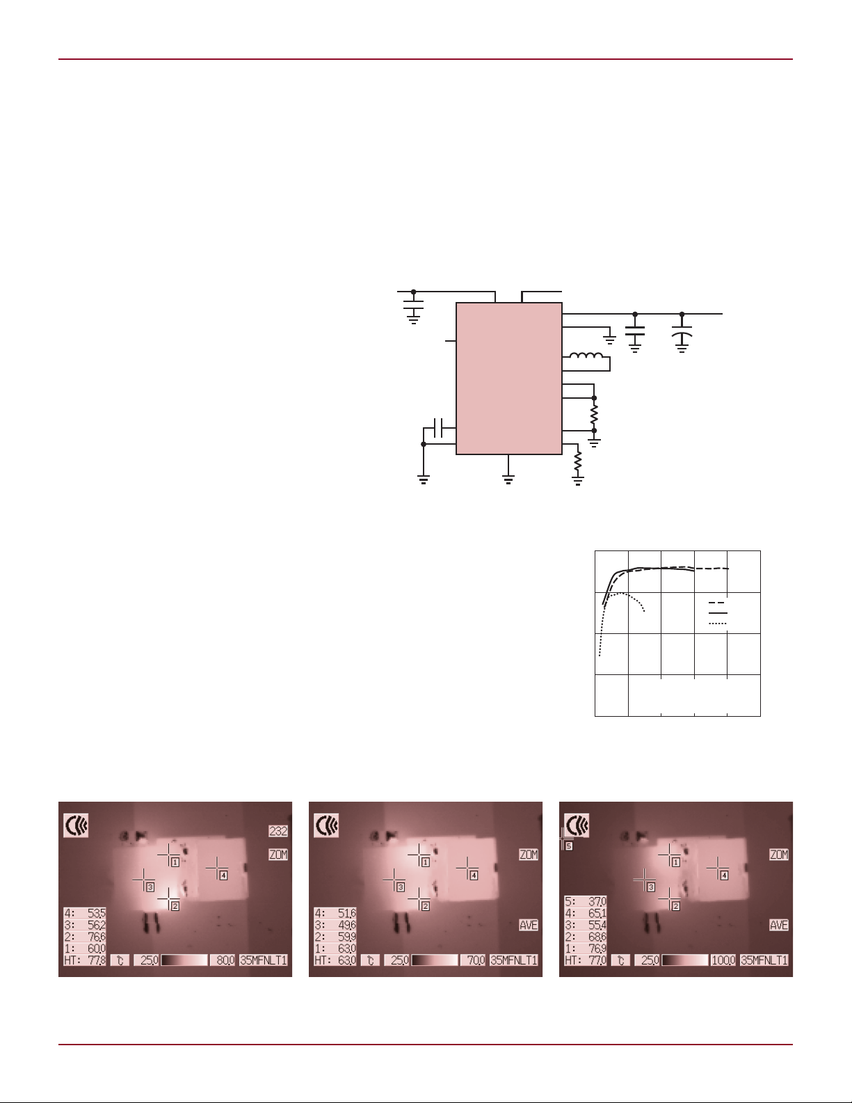
DESIGN IDEAS L
V
OUT
FCB
RUN
SW1
SW2
R
SENSE
SENSE
–
SS
V
FB
SGND
PLLIN
LTM4609
L1
3.4µH
2.74k
10µF
×2
35V
150µF
×2
35V
V
OUT
30V
3A
OPTIONAL
CLOCK SYNC
L1: SUMIDA CDEP147
V
IN
PGND
V
IN
10V TO 36V
10nF
4.7µF
×2
50V
+
ON/OFF
SENSE
+
7mΩ
EFFICIENCY (%)
LOAD CURRENT (A)
100
100
80
2 4 6 8
90
85
95
CONTINUOUS CURRENT MODE
V
OUT
= 30V
fSW = 275kHz
36V
IN
24V
IN
10V
IN
µModule Regulator Fits a (Nearly)
Complete Buck-Boost Solution
in 15mm × 15mm × 2.8mm for
4.5V–36V V
to 0.8V–34V V
IN
Introduction
Linear Technology offers a number of
high efficiency synchronous 4-switch
buck-boost DC/DC converter solutions for applications where V
OUT
falls
within the range of VIN. The LTM4605,
LTM4607 and LTM4609 µModule
regulators are nearly self-contained
buck-boost solutions that share pincompatible 15mm × 15mm × 2.8mm
packages. The package includes the
controller, four power FETs and a
number of other discrete components.
Only an external inductor, a sensing
resistor, a voltage setting resistor and
a few input and output capacitors are
needed to complete a high efficiency
buck-boost converter.
Table 1 shows the input voltage,
output voltage and current specifications of these three buck-boost
µModule regulators. The LTM4609
is the latest addition to this family.
It satisfies the needs of high output
voltage applications with an output
range of 0.8V–34V.
High Performance with
Minimum Component Count
As with all Linear Technology µModule
regulators, the LTM4609 requires only
OUT
by Judy Sun, Sam Young and Henry Zhang
Figure 1. Just a few components form a complete 10V to 36V input, 30V/3A output converter
using the LTM4609.
a few external components to complete
a wide input range buck-boost converter. Figure 1 shows a 10V to 36V
input, 30V output design. The output
current capability is 3A at 10V VIN,
and 8A with 36V input.
Figure 2 shows the efficiency of
this converter, up to 98% in buck
mode and 95% in boost mode. The
low profile LGA package features low
thermal resistance from junction to
pin, thus maintaining an acceptable
junction temperature even at high
output power. The LTM4609’s high
Figure 2. Efficiency of the 30V
buck-boost converter
OUT
= 30V, I
= 6A VIN = 12V, V
OUT
OUT
= 30V, I
OUT
= 3A
3939
VIN = 36V, V
Figure 3. Thermal-graph taken with the LTM4609 running at different input voltages. The LTM4609 is on the left, the inductor (Sumida CDEP147)
is on the right. No heat sink or forced air flow. Ambient temperature = 25°C.
Linear Technology Magazine • March 2009
OUT
= 30V, I
= 8A VIN = 24V, V
OUT

L DESIGN IDEAS
V
IN
GND
LTM4609
L1
L2
C
IN1
10µF
C
BULK
100µF
V
IN
+
C
IN2
10µF
L1,L2: FAIR-RITE 2518065007Y6
V
IN
200mV/DIV
10µs/DIV
VIN = 10V
V
OUT
= 30V
I
OUT
= 3A
C
BULK
= 100µF
C
IN1
, C
IN2
= 4.7µF
V
IN
200mV/DIV
10µs/DIV
VIN = 10V
V
OUT
= 30V
I
OUT
= 3A
C
BULK
= 100µF
C
IN1
, C
IN2
= 10µF
L1, L2: FAIR-RITE 2518065007Y6
efficiency combined with its excellent
thermal management capability enables it to deliver up to 240W output
power without a heat sink or forced
airflow. Figure 3 shows the thermalgraphs taken with three different input
voltages and loads at 25°C ambient
temperature. With 240W output and
36V input, the maximum temperature
rise of the LTM4609 is only 52.8°C.
Input Ripple Reduction
One way to improve efficiency in a
switching DC/DC converter is to minimize the turn-on and turn-off times
of the MOSFET—shorter transitions
correspond to lower switch losses.
However, fast transitions also lead
to high frequency switching noise,
which can pollute the input power
source. For the applications where the
input voltage ripple must be limited,
a simple LC π filter can be inserted at
the input side to attenuate the high
frequency input voltage noise. Figure
4 shows the LTM4609 with an input
π filter. The filter includes two 10µF
low ESR ceramic capacitors and two
very small magnetic beads. For lower
output power applications, only one
magnetic bead is necessary.
Figure 5 shows the input ripple
reduction with the π filter. Figure 5a
shows the input ripple with 100µF
aluminum electrolytic plus 2 × 4.7µF
Table 1. Specification comparison of the LTM4605, LTM4607 and LTM4609
LTM4605 LTM4607 LTM4609
V
IN
V
OUT
I
OUT
Package 15mm × 15mm × 2.8mm LGA
4.5V ~ 20V 4.5V ~ 36V 4.5V ~ 36V
0.8V ~ 16V 0.8V ~ 24V 0.8V ~ 34V
5A
(12A in buck mode)
(10A in buck mode)
5a. Input voltage waveform without
the input π filter shown in Figure 4
ceramic input capacitors. Figure 5b
shows the input ripple with the filter
shown in Figure 4. Both waveforms
are measured across the 100µF aluminum capacitor. A 67% reduction in
input ripple is obtained with the input
π filter, which requires only two small
additional magnetic beads.
5A
Figure 4. The LTM4609 µModule regulator with an input π filter.
5b. Input voltage waveform with
input π filter as shown in Figure 4
Figure 5. The input π filter shown in Figure 4 effectively reduces
the input voltage spike caused by switching action of the MOSFETs.
Conclusion
Buck-boost µModule regulators
are easy-to-use, high performance
solutions for applications where a
regulated output voltage sits within the
range of the input voltage. The 15mm
× 15mm × 2.8mm LTM4609 widens the
input/output voltage range of the pin
compatible LTM4605 and LTM4607.
The advanced package technology, as
well as the high efficiency design of
the LTM4609, allows it to deliver up
to 240W of output power without heat
sinks or forced airflow. For applica-
4A
(10A in buck mode)
tions that require low input voltage
ripple, a simple π filter can be added
by inserting one or two small magnetic
beads to significantly reduce the high
frequency input noise.
L
LT3755/56, continued from page 32
PWM on- and off-times are 1µs as
with the other circuits. Figure 7 shows
the waveforms during a short circuit
fault on the output. The input current remains in control as the switch
current ramps up to the set limit of
10A, then skips the next few cycles
while the current sensed by the LED
40
40
resistor ramps down to 1.5A. This
faulted mode of circuit operation can
continue indefinitely without damage
to the components.
Conclusion
The LT3755 and LT3756 offer unparalleled performance for an LED
controller generating PWM pulse
widths as narrow as 1µs, which
enables 50:1 PWM dimming at frequencies above the audible range.
Other features include open LED
protection, an open LED status indicator, and programmability of the LED
current via an analog input.
Linear Technology Magazine • March 2009
L

New Device Cameos
NEW DEVICE CAMEOS L
Micropower Low Noise Boost
Converter with Output
Disconnect
The LT3495/LT3495B/LT3495-1/
LT3495B-1 is a low noise boost converter with integrated power switch,
feedback resistor and output disconnect circuitry. The part controls power
delivery by varying both the peak
inductor current and switch off-time.
This new control scheme results in low
output voltage ripple as well as high
efficiency over a wide load range.
For the LT3495/LT3495-1, the
off-time of the switch is not allowed
to exceed a fixed level, guaranteeing
the switching frequency stays above
the audio band for the entire load
range. This feature is disabled for the
LT3495B/LT3495B-1, which leads to
higher efficiency at light load. The difference between the LT3495/LT3495B
and LT3495-1/LT3495B-1 is the
level of the switch current limit. The
LT3495/LT3495B has a typical peak
current limit of 650mA while the
LT3495-1/LT3495B-1 has a typical
peak current limit of 350mA.
The LT3495 series has an output
disconnect PMOS that blocks the
load from the input during shutdown.
During normal operation, the maximum current through this PMOS is
limited by circuitry inside the chip,
which helps the chip survive output
shorts.
The input voltage range of the
LT3495 series is a wide 2.5V to 16V
and the output voltage can be up
to 40V. In addition, the part is well
compensated internally, and can be
stable with very small ceramic output
capacitors.
Other features include low quiescent current (60µA in active mode and
0.1µA in shutdown mode), integrated
output dimming, maximum switching
on-time and undervoltage lockout.
Combining the small ceramic capaci-
tors and space saving 10-pin 3mm ×
2mm DFN packages, the LT3495
enables compact solutions for many
applications.
Dual 550mA, 1MHz
Synchronous Boost Regulator
with Output Disconnect in a
3mm × 3mm DFN
The LTC3535 is a dual-channel 1MHz,
current mode synchronous boost
DC/DC converter with integrated
output disconnect and soft-start. The
LTC3535’s internal 550mA switches
deliver output voltages as high as
5.25V from an input voltage range of
0.7V at start-up/0.5V when running
to 5V, making it ideal for single- or
multicell alkaline/NiMH as well as Liion/polymer applications. Each of the
LTC3535’s channels has it own power
input and is completely independent,
offering maximum design flexibility.
For example, one channel can deliver
up to 50mA of continuous output current at 3.3V while the other channel
delivers up to 100mA at 1.8V to power
a microcontroller from a single alkaline
cell. The 1MHz switching frequency
minimizes external component sizes
while providing up to 94% efficiency.
Combined with a compact 3mm × 3mm
DFN-12 package, the LTC3535 dual
channel boost provides the tiny and
efficient solution footprint required in
handheld applications.
Burst Mode
quiescent current to only 18µA (both
channels), providing extended battery
run time in handheld applications. The
LTC3535 is an ideal part for handheld
dual boost applications where small
solution size and maximum battery
run time are defining factors.
®
operation lowers
Ideal Diode Equipped High
Power Battery Charger
Handles All Chemistries
The LTC4012, LTC4012-1, LTC4012-2
and LTC4012-3 are a family of high
power buck battery chargers all in a
20-lead 4mm × 4mm QFN package.
Compared to the LTC4009 family of
chargers, the 4012 family adds Ideal
Diode™ input reverse current input
protection and extends the high
efficiency to higher current levels.
Combined with just a few external
components and external termination
control, the LTC4012 family facilitates
construction of chargers capable of
delivering up to 4A to batteries with
output power levels approaching 66W
in a very small footprint.
the proven quasi-constant frequency,
constant off-time PWM buck control architecture as found in Linear
Technology’s LTC4008. This unique
buck topology provides continuous
switching with synchronous rectification even with no load current,
critical to preventing audible noise
in constant voltage charge termination applications. However, LTC4012
family uses switching NFETs along
with an adaptive gate drive to avoid
overlap conduction losses. The higher
550kHz switching frequency reduces
both the inductor size and output
capacitance requirements while offering efficiencies up to 95% or more.
If the duty cycle goes below 20% or
above 80%, the LTC4012 lowers the
switching frequency to avoid pulse
skipping that might otherwise begin to
occur at 550kHz. Under low dropout
conditions requiring high duty cycle
operation, the internal watchdog timer
prevents the LTC4012 from switching
below 25kHz, achieving a maximum
duty cycle of 98% without producing
audible noise. There is also an input
current monitor function that prevents
input power overload when the input
power is shared with a load.
LTC4012. The LTC4012 and LTC40123 offer a user programmable voltage set
point using an external resistor divider
allowing for multi-chemistry support.
The Li-ion optimized LTC4012-1 and
LTC4012-2 support one to four series
cells via pin selection. The LTC40121 provides 4.1V/cell charging while
the LTC4012-2 produces 4.2V/cell.
Output voltage accuracy is typically
±0.5% and a maximum of ±0.8% over
temperature. These ICs contain a
switch that in shutdown removes voltage divider current drained from the
The LTC4012 family builds upon
There are four versions of the
Linear Technology Magazine • March 2009
4141

L NEW DEVICE CAMEOS
EFFICIENCY (%)
INPUT DC VOLTAGE (V)
200100
100
70
120 140 160 180
75
80
90
85
95
P
OUT
= 63W
P
OUT
= 48W
P
OUT
= 25W
OUTPUT VOLTAGE ERROR (V)
I
OUT
(mA)
2500
–0.5
–0.25
0
0.25
0.5
10050 150 200
battery whether external or internal.
Programming the charge current only
requires a single external resistor.
The fault management system of the
LTC4012 family suspends charging
immediately for various conditions.
First is battery overvoltage protection,
which can occur with the sudden loss
of battery load during bulk charge.
Second, each IC features internal
over-temperature protection to prevent silicon damage during elevated
thermal operation.
The LTC4012 family has a logic-level
shutdown control input and three
open-drain status outputs. First is an
input current limit (ICL) status flag to
tell the system when VIN is running at
over 95% of its current capacity. The
input current limit accuracy is typically ±3% and a maximum of ±4% over
the full operating temperature range.
Next is the AC present status, which
indicates when VIN is within a valid
range for charging under all modes of
operation. The last is a charge status
output can indicate bulk or C/10
charge states. The control input and
status outputs of the LTC4012, along
with the analog current monitor output, can be used by the host system
to perform necessary preconditioning,
charge termination and safety timing
functions.
4MHz Synchronous StepDown DC/DC Converter
Delivers up to 1.25A from a
3mm × 3mm DFN
The LTC3565 is a high efficiency synchronous step-down regulator that
can deliver up to 1.25A of continuous
output current from a 3mm × 3mm
DFN (or MSOP-10E) package. Using
a constant frequency of (up to 4MHz)
and current mode architecture, the
LTC3565 operates from an input voltage range of 2.5V to 5.5V making it
ideal for single cell Li-Ion, or multicell
Alkaline/NiCad/NiMH applications.
It can generate output voltages as
low as 0.6V, enabling it to power the
latest generation of low voltage DSPs
and microcontrollers. An independent
RUN pin enables simple turn-on and
shutdown. Its switching frequency
is user programmable from 400kHz
to 4MHz, enabling the designer to
optimize efficiency while avoiding critical noise-sensitive frequency bands.
The combination of its 3mm × 3mm
DFN-10 (or MSOP-10) package and
high switching frequency keeps external inductors and capacitors small,
providing a very compact, thermally
efficient footprint.
The LTC3565 uses internal switches
with an R
of only 0.13Ω (N-Chan-
DS(ON)
nel lower FET) and 0.15Ω (P-Channel
upper FET) to deliver efficiencies
as high as 95%. It also utilizes low
dropout 100% duty cycle operation
to allow output voltages equal to VIN,
further extending battery run time.
The LTC3565 utilizes Automatic Low
Ripple ( < 25mV
) Burst Mode®
P–P
operation to offer only 40µA no load
quiescent current. If the application is
noise sensitive, Burst Mode operation
can be disabled using a lower noise
pulse-skipping mode, which still offers
only 330µA of quiescent current. The
LTC3565 can be synchronized to an
external clock throughout its entire
frequency range. Other features include ±2% output voltage accuracy and
over-temperature protection.
L
LT3751, continued from page 13
LT3751 controller, and the optocoupler
on the feedback resistor divider. The
auxiliary windings provide the desired
galvanic isolation boundary while
maintaining an isolated feedback path
from the output node to the LT3751
FB pin. Figures 12 and 13 show the
regulator’s performance.
The fully isolated, high voltage input/output regulator yields over 90%
efficiency. Load regulation is excellent
as shown in Figure 13b, due mainly
to the added gain of the optocoupler
circuit.
Conclusion
The ability to run from any input
supply voltage ranging from 4.75V
to greater than 400V and the abundance of safety features make the
LT3751 an excellent choice for high
voltage capacitor chargers or high
voltage regulated power supplies. In
fact, the LT3751 is, for now, the only
42
42
a. Efficiency b. Load regulation
Figure 13. Fully isolated, high voltage regulator performance
boundary-mode capacitor charger
controller that can accurately operate
from extremely high input voltages.
The LT3751 simplifies design by integrating many functions that—due
to cost and board real-estate—would
otherwise not be realizable. Although
LT3751 includes many more features
than we can show in one article. We
recommended consulting the data
sheet or calling the Linear Technology
applications engineering department
for more in-depth coverage of all available features.
L
several designs are shown here, the
Linear Technology Magazine • March 2009

www.linear.com
DESIGN TOOLS L
MyLinear
(www.linear.com/mylinear)
MyLinear is a customizable home page to store your
favorite LTC products, categories, product tables, contact
information, preferences and more. Creating a MyLinear
account allows you to…
• Store and update your contact information. No more
reentering your address every time you request a
sample!
• Edit your subscriptions to Linear Insider email
newsletter and Linear Technology magazine.
• Store your favorite products and categories for future
reference.
• Store your favorite parametric table. Customize a table
by editing columns, filters and sort criteria and store
your settings for future use.
• View your sample history and delivery status.
Using your MyLinear account is easy. Just visit
www.linear.com/mylinear to create your account.
Purchase Products
(www.linear.com/purchase)
Purchase products directly from Linear Technology either
through the methods below or contact your local Linear
sales representative or licensed distributor.
Credit Card Purchase — Your Linear Technology parts
can be shipped almost anywhere in the world with
your credit card purchase. Orders up to 500 pieces
per item are accepted. You can call (408) 433-5723
or email orders@linear.com with questions regarding
your order.
Linear Express — Purchase online with credit terms.
Linear Express is your new choice for purchasing any
quantity of Linear Technology parts. Credit terms are
available for qualifying accounts. Minimum order is
only $250.00. Call 1-866-546-3271 or email us at
express@linear.com.
Subscribe!
Subscribe to
Linear Technology magazine at
www.linear.com/mylinear
Product and Applications
Information
At www.linear.com you will find our complete collection
of product and applications information available for
download. Resources include:
Data Sheets — Complete product specifications,
applications information and design tips
Application Notes — In depth collection of solutions,
theory and design tips for a general application area
Design Notes — Solution-specific design ideas and
circuit tips
LT Chronicle — A monthly look at LTC products for
specific end-markets
Product Press Releases — New products are announced
constantly
Solutions Brochures — Complete solutions for automotive electronics, high speed ADCs, LED drivers, wireless
infrastructure, industrial signal chain, handheld, battery
charging, and communications and industrial DC/DC
conversion applications.
Product Selection
The focus of Linear Technology’s website is simple—to
get you the information you need quickly and easily. With
that goal in mind, we offer several methods of finding the
product and applications information you need.
Part Number and Keyword Search — Search Linear
Technology’s entire library of data sheets, Application
Notes and Design Notes for a specific part number or
keyword.
Sortable Parametric Tables — Any of Linear Technology’s product families can be viewed in table form,
allowing the parts to be sorted and filtered by one or
many functional parameters.
Applications Solutions — View block diagrams for a
wide variety of automotive, communcations, industrial
and military applications. Click on a functional block to
generate a complete list of Linear Technology’s product
offerings for that function.
Design Support
Packaging (www.linear.com/packaging) — Visit our
packaging page to view complete information for all of
Linear Technology’s package types. Resources include
package dimensions and footprints, package cross
reference, top markings, material declarations, assembly
procedures and more.
Quality and Reliability (www.linear.com/quality)
— The cornerstone of Linear Technology’s Quality,
Reliability & Service (QRS) Program is to achieve 100%
customer satisfaction by producing the most technically
advanced product with the best quality, on-time delivery
and service. Visit our quality and reliability page to view
complete reliability data for all of LTC’s products and
processes. Also available is complete documentation on
assembly and manufacturing flows, quality and environmental certifications, test standards and documentation
and failure analysis policies and procedures.
Lead Free (www.linear.com/leadfree) — A complete
resource for Linear Technology’s Lead (Pb) Free Program
and RoHS compliance information.
Simulation & Software
Linear Technology offers several powerful simulation
tools to aid engineers in designing, testing and troubleshooting their high performance analog designs.
LTspice/SwitcherCAD™ III (www.linear.com/swcad)
— LTspice / SwitcherCAD III is a powerful SPICE simulator and schematic capture tool specifically designed
to speed up and simplify the simulation of switching
regulators. LTspice / SwitcherCAD III includes:
• Powerful general purpose Spice simulator with
schematic capture, waveform viewing, and speed
enhancements for switching regulators.
• Complete and easy to use schematic capture and
waveform viewer.
• Macromodels for most of Linear Technology’s
switching regulators as well as models for many of
Liinear’s high performance linear regulators, op amps,
comparators, filters and more.
• Ready to use demonstration circuits for over one hundred of Linear Technology’s most popular products.
FilterCAD — FilterCAD 3.0 is a computer-aided design
program for creating filters with Linear Technology’s
filter ICs.
Noise Program — This program allows the user to calculate circuit noise using Linear Technology op amps to
determine the best op amp for low noise applications.
SPICE Macromodel Library — The Library includes
Linear op amp SPICE macromodels for use with any
SPICE simulation package.
Linear Technology Magazine • March 2009
4343

SALES OFFICES
NORTH AMERICA
NORTHERN CALIFORNIA /
NEVADA
Bay Area
720 Sycamore Dr.
Milpitas, CA 95035
Tel: (408) 428-2050
Fax: (408) 432-6331
Sacramento / Nevada
2260 Douglas Blvd., Ste. 280
Roseville, CA 95661
Tel: (916) 787-5210
Fax: (916) 787-0110
PACIFIC NORTHWEST
Denver
7007 Winchester Cir., Ste. 130
Boulder, CO 80301
Tel: (303) 926-0002
Fax: (303) 530-1477
Portland
5005 SW Meadows Rd., Ste. 410
Lake Oswego, OR 97035
Tel: (503) 520-9930
Fax: (503) 520-9929
Salt Lake City
Tel: (801) 731-8008
Seattle
2018 156th Ave. NE, Ste. 100
Bellevue, WA 98007
Tel: (425) 748-5010
Fax: (425) 748-5009
SOUTHWEST
Los Angeles
21243 Ventura Blvd., Ste. 238
Woodland Hills, CA 91364
Tel: (818) 703-0835
Fax: (818) 703-0517
Orange County
15375 Barranca Pkwy., Ste. A-213
Irvine, CA 92618
Tel: (949) 453-4650
Fax: (949) 453-4765
Phoenix
2085 E. Technology Cir., Ste. 101
Tempe, AZ 85284
Tel: (480) 777-1600
Fax: (480) 838-1104
San Diego
5090 Shoreham Place, Ste. 110
San Diego, CA 92122
Tel: (858) 638-7131
Fax: (858) 638-7231
CENTRAL
Chicago
2040 E. Algonquin Rd., Ste. 512
Schaumburg, IL 60173
Tel: (847) 925-0860
Fax: (847) 925-0878
Cleveland
7550 Lucerne Dr., Ste. 106
Middleburg Heights, OH 44130
Tel: (440) 239-0817
Fax: (440) 239-1466
Columbus
Tel: (614) 488-4466
Detroit
39111 West Six Mile Road
Livonia, MI 48152
Tel: (734) 779-1657
Fax: (734) 779-1658
Indiana
Tel: (317) 581-9055
Iowa
Tel: (319) 393-5763
Kansas
Tel: (913) 829-8844
Minneapolis
7805 Telegraph Rd., Ste. 225
Bloomington, MN 55438
Tel: (952) 903-0605
Fax: (952) 903-0640
Wisconsin
Tel: (262) 859-1900
NORTHEAST
Boston
15 Research Place
North Chelmsford, MA 01863
Tel: (978) 656-4750
Fax: (978) 656-4760
Connecticut
Tel: (860) 228-4104
Philadelphia
3220 Tillman Dr., Ste. 120
Bensalem, PA 19020
Tel: (215) 638-9667
Fax: (215) 638-9764
SOUTHEAST
Atlanta
Tel: (770) 888-8137
Austin
8500 N. Mopac, Ste. 603
Austin, TX 78759
Tel: (512) 795-8000
Fax: (512) 795-0491
Dallas
17000 Dallas Pkwy., Ste. 200
Dallas, TX 75248
Tel: (972) 733-3071
Fax: (972) 380-5138
Fort Lauderdale
Tel: (954) 473-1212
Houston
1080 W. Sam Houston Pkwy.,
Ste. 225
Houston, TX 77043
Tel: (713) 463-5001
Fax: (713) 463-5009
Huntsville
Tel: (256) 881-9850
Orlando
Tel: (407) 688-7616
Raleigh
15100 Weston Pkwy., Ste. 202
Cary, NC 27513
Tel: (919) 677-0066
Fax: (919) 678-0041
Tampa
Tel: (813) 634-9434
CANADA
Calgary, AB
Tel: (403) 455-3577
Montreal, QC
Tel: (450) 689-2660
Ottawa, ON
Tel: (613) 421-3090
Toronto, ON
Tel: (440) 239-0817
Vancouver, BC
Tel: (604) 729-1204
ASIA
AUSTRALIA / NEW ZEALAND
Linear Technology Corporation
133 Alexander Street
Crows Nest NSW 2065
Australia
Tel: +61 (0)2 9432 7803
Fax: +61 (0)2 9439 2738
CHINA
Linear Technology Corp. Ltd.
Units 1503-04, Metroplaza
Tower 2
223 Hing Fong Road
Kwai Fong, N.T., Hong Kong
Tel: +852 2428-0303
Fax: +852 2348-0885
Linear Technology Corp. Ltd.
Room 2701, City Gateway
No. 398 Cao Xi North Road
Shanghai, 200030, PRC
Tel: +86 (21) 6375-9478
Fax: +86 (21) 5465-5918
Linear Technology Corp. Ltd.
Room 816, 8/F
China Electronics Plaza B
No. 3 Dan Ling Rd., Hai Dian
District
Beijing, 100080, PRC
Tel: +86 (10) 6801-1080
Fax: +86 (10) 6805-4030
Linear Technology Corp. Ltd.
Room 2604, 26/F
Excellence Times Square Building
4068 YiTian Road, Futian District
Shenzhen, 518048, PRC
Tel: +86 755-8236-6088
Fax: +86 755-8236-6008
To subscribe to Linear Technology magazine, visit www.linear.com/mylinear
EUROPE
JAPAN
Linear Technology KK
8F Shuwa Kioicho Park Bldg.
3-6 Kioicho Chiyoda-ku
Tokyo, 102-0094, Japan
Tel: +81 (3) 5226-7291
Fax: +81 (3) 5226-0268
Linear Technology KK
6F Kearny Place Honmachi Bldg.
1-6-13 Awaza, Nishi-ku
Osaka-shi, 550-0011, Japan
Tel: +81 (6) 6533-5880
Fax: +81 (6) 6543-2588
Linear Technology KK
7F, Sakuradori Ohtsu KT Bldg.
3-20-22 Marunouchi, Naka-ku
Nagoya-shi, 460-0002, Japan
Tel: +81 (52) 955-0056
Fax: +81 (52) 955-0058
KOREA
Linear Technology Korea Co.,
Ltd.
Yundang Building, #1002
Samsung-Dong 144-23
Kangnam-Ku, Seoul 135-090
Korea
Tel: +82 (2) 792-1617
Fax: +82 (2) 792-1619
SINGAPORE
Linear Technology Pte. Ltd.
507 Yishun Industrial Park A
Singapore 768734
Tel: +65 6753-2692
Fax: +65 6752-0108
TAIWAN
Linear Technology Corporation
8F-1, 77, Nanking E. Rd., Sec. 3
Taipei, Taiwan
Tel: +886 (2) 2505-2622
Fax: +886 (2) 2516-0702
1-800-4-LINEAR • 408-432-1900 • 408-434-0507 (fax)
FINLAND
Linear Technology AB
Teknobulevardi 3-5
P.O. Box 35
FIN-01531 Vantaa
Finland
Tel: +358 (0)46 712 2171
Fax: +358 (0)46 712 2175
FRANCE
Linear Technology S.A.R.L.
Parc Tertiaire Silic
2 Rue de la Couture, BP10217
94518 Rungis Cedex
France
Tel: +33 (1) 56 70 19 90
Fax: +33 (1) 56 70 19 94
GERMANY
Linear Technology GmbH
Osterfeldstrasse 84, Haus C
D-85737 Ismaning
Germany
Tel: +49 (89) 962455-0
Fax: +49 (89) 963147
Linear Technology GmbH
Haselburger Damm 4
D-59387 Ascheberg
Germany
Tel: +49 (2593) 9516-0
Fax: +49 (2593) 951679
Linear Technology GmbH
Jesinger Strasse 65
D-73230 Kirchheim/Teck
Germany
Tel: +49 (0)7021 80770
Fax: +49 (0)7021 807720
ITALY
Linear Technology Italy Srl
Orione 3, C.D. Colleoni
Via Colleoni, 17
I-20041 Agrate Brianza (MI)
Italy
Tel: +39 039 596 5080
Fax: +39 039 596 5090
SWEDEN
Linear Technology AB
Electrum 204
Isafjordsgatan 22
SE-164 40 Kista
Sweden
Tel: +46 (8) 623 16 00
Fax: +46 (8) 623 16 50
UNITED KINGDOM
Linear Technology (UK) Ltd.
3 The Listons, Liston Road
Marlow, Buckinghamshire
SL7 1FD
United Kingdom
Tel: +44 (1628) 477066
Fax: +44 (1628) 478153
Linear Technology Corporation
1630 McCarthy Blvd.
Milpitas, CA 95035-7417
www.linear.com
© 2009 Linear Technology Corporation/Printed in U.S.A./42.6K
Linear Technology Magazine • March 2009
 Loading...