

L DESIGN FEATURES
V
IN
SV
IN
SW
RUN
PLLLPF
TRACK
V
OUT
FB
I
TH
I
THM
PGOOD
MGN
CLKOUT GND
CLKIN
4.87k
100μF
10μF
V
OUT
1.8V
8A
V
IN
3V TO 5.5V
LTM4608
SGND
V
IN
V
IN
V
IN
3.3V
PGOOD
COMP
LTM4604
RUN/SS
2.37k
22MF
6.3V
r2
V
OUT
2.5V
4A
10MF
6.3V
V
OUT
FB
TRACK
GND
LOAD CURRENT (A)
0
70
EFFICIENCY (%)
75
80
85
90
95
100
1.0 2.0 3.0 4.0
V
OUT
= 2.5V
VIN = 3.3V
Low Voltage, High Current Step-Down
µModule Regulators Put a (Nearly)
Complete Power Supply in a
15mm × 9mm × 2.8mm Package
by Judy Sun, Sam Young and Henry Zhang
Introduction
Endlessly increasing power density
requirements are a major driving force
behind the continuous need to find
new power supply solutions. Switching
regulators are the top choice for high
current applications because of their
high efficiency and high performance,
but high power density doesn’t come
for free with a switcher. Components
must be carefully chosen and laid
out to maximize efficiency, transient
response and thermal performance.
Making a high density switching power
supply requires significant design and
test time, or does it?
The LTM4604 and LTM4608 LTC
µModule switching regulators make
it possible to create high density
designs with minimal effort. Both
are high density power supplies for
≤5.5V input voltage, high output current, step-down applications. Each
µModule regulator comes in a 15mm
× 9mm LGA surface mount package
and is nearly self-contained—only a
few passive components are required
to complete a power supply design. The
switching controller, MOSFETs, inductor and all support components are
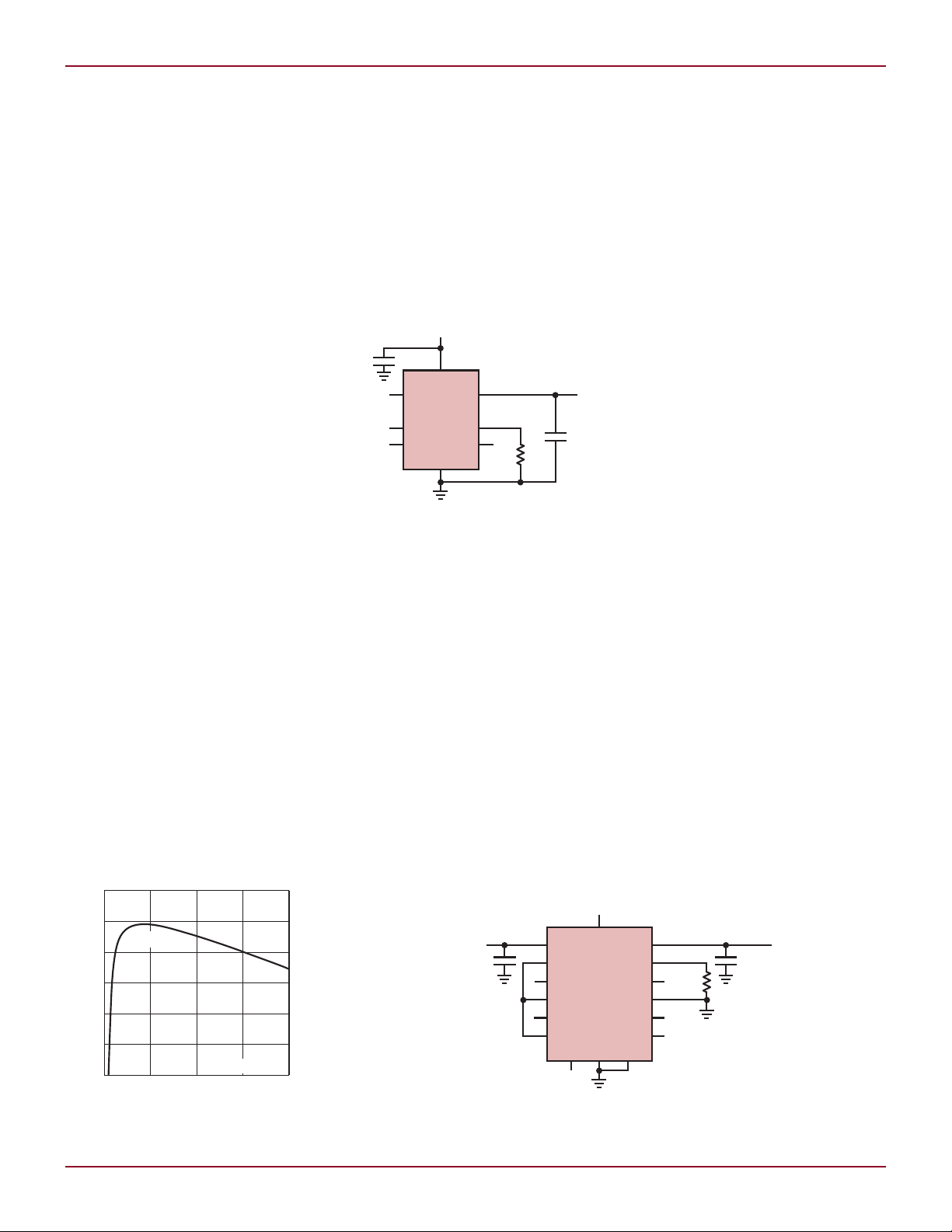
Figure 1. Only a few components are required
for a 2.5V/4A design with LTM4604.
already carefully chosen and laid out
in the package. Low profile packages
(2.3mm and 2.8mm, respectively) allow
them to be easily mounted in unused
space on the bottom of PC boards and
simplify thermal management.
The LTM4604 features a 2.375V
to 5.5V input range and a 0.8V to
5V output range, while the LTM4608
takes a 2.7V to 5.5V input to a 0.6V to
5V output. The LTM4604 can deliver
up to 4A continuous current with up
to 95% efficiency. The slightly higher
profile of the LTM4608 allows it to
deliver up to 8A continuous current
thanks to its high efficiency design and
low thermal impedance package.
Easy Design with
Few Components
Figure 1 shows a typical 2.5V/4A
design with LTM4604 and Figure 2
shows the resulting efficiency. Ceramic
input capacitors are integrated into
the µModule package—additional
input capacitors are only required if
a load step is expected up to the full
4A level. Additional required output
capacitance is typically in the range
of 22µF to 100µF. A single resistor on
the FB pin sets the output voltage.
For applications needing more
output current, the LTM4608 fits the
bill. Figure 3 shows a 1.8V/8A design
with LTM4608 and Figure 4 shows
its efficiency. As with the LTM4604,
the number of necessary external
components has been reduced to a
minimum, significantly simplifying
the design effort. Nevertheless, a very
fast transient response to the line and
load changes is guaranteed by the optimized design of the µModule’s high
switching frequency and current mode
control architecture. Furthermore, a
number of features can be enabled on
the LTM4604 and LTM460408 to suit
the needs of various applications.
Figure 2. High efficiency is achieved with the
LTM4604 in the application of Figure 1
28
Figure 3. Only a few components are required for a 1.8V/8A design with the LTM4608.
Linear Technology Magazine • September 2008
LOAD CURRENT (A)
0
70
EFFICIENCY (%)
75
80
85
90
95
100
2 4 6 8
10
V
OUT
= 1.8V
V
IN
= 5V
VIN = 3.3V
TOTAL LOAD CURRENT (A)
0 2 4 6 8 10 12 14 16 18
0
1
2
3
4
5
6
7
8
9
OUTPUT CURRENT OF EACH LTM4608 (A)
I
OUT1
I
OUT2
V
IN
SV
IN
SW
RUN
PLLLPF
TRACK
MODE
PHMODE
V
OUT
FB
I
TH
I
THM
PGOOD
BSEL
MGN
CLKOUT GND
CLKIN
100µF
6.3V
X5R
100pF
10µF
3.32k
V
OUT
1.5V
16A
V
IN
3V TO 5.5V
LTM4608
SGND
V
IN
SV
IN
SW
RUN
PLLLPF
TRACK
MODE
PHMODE
V
OUT
FB
I
TH
I
THM
PGOOD
BSEL
MGN
CLKOUT GND
CLKIN
10µF
100µF
6.3V
X5R
LTM4608
SGND
Figure 4. High efficiency is achieved with the
LTM4608 in the application of Figure 3.
Wealth of Features
Both LTM4604 and LTM4608 feature RUN pin control, output voltage
tracking selections and power good
indicators. For systems requiring
voltage sequencing between different
power supplies, the sequencing function can be implemented by controlling
the RUN pins and the PGOOD signals
with a few additional components.
Fault protection features include
overvoltage protection, over current
protection and thermal shutdown.
The LTM4608 offers some additional features. Burst Mode® operation,
pulse-skipping mode or continuous
current mode can be selected to improve light load efficiency. Burst Mode
operation provides the highest efficiency at very light load, while forced
continuous current mode leads to the
lowest output ripple. Pulse-skipping
mode offers a compromise between
Burst Mode operation and continuous
mode, offering good light load efficiency
while keeping output voltage ripple
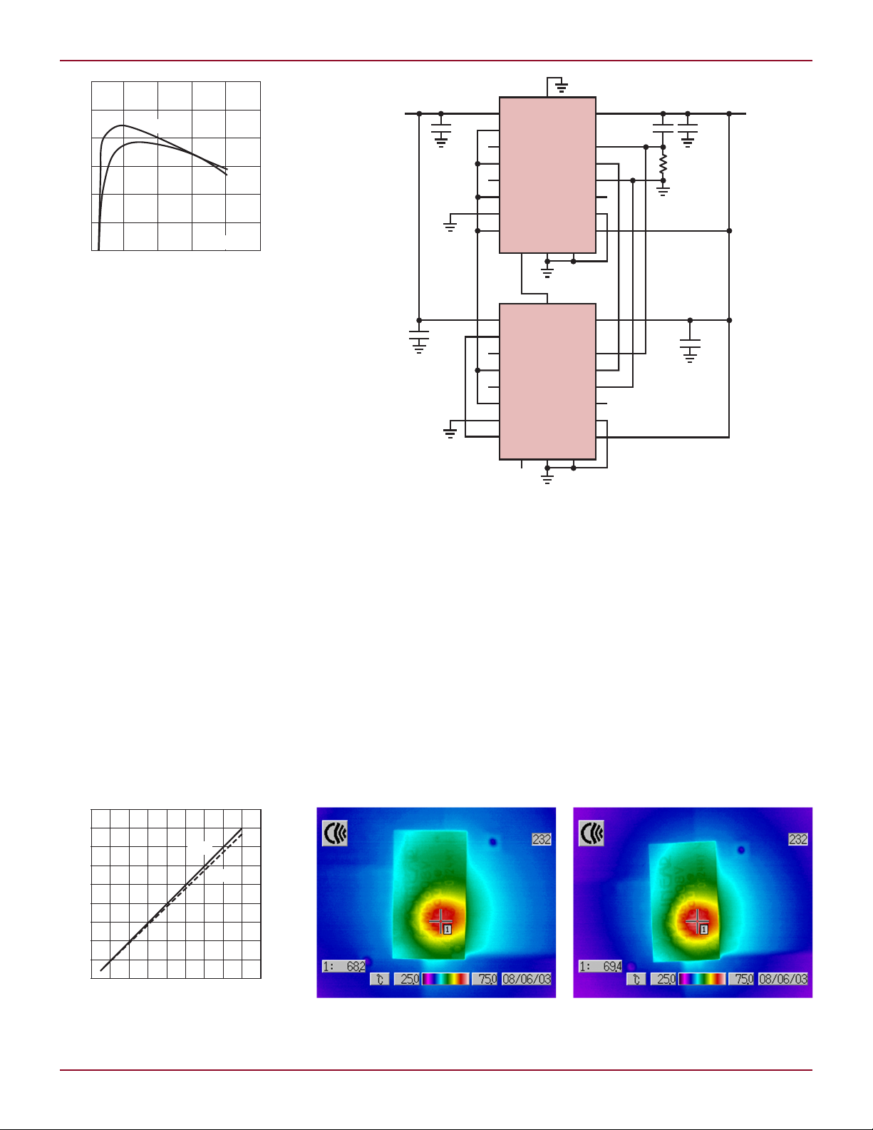
Figure 5. Two LTM4608s are easily paralleled to provide
1.5V/16A output with interleaved switching operation.
down. Programmable output voltage
margining is supported for ±5%, ±10%
and ±15% levels. The LTM4608 also
allows frequency synchronization and
spread spectrum operation to further
reduce switching noise harmonics.
Parallel for More Power
With cycle-by-cycle current mode
control, the LTM4604 and LTM4608
can be easily paralleled to provide
more output power with excellent current sharing. The LTM4608 includes
CLKIN and CLKOUT pins to make it
DESIGN FEATURES L
possible to operate paralleled devices
out of phase of one another to reduce
input and output ripple. A total of 12
phases can be cascaded to run simultaneously with respect to each other
by programming the PHMODE pin of
each LTM4608 to different levels.
Figure 5 shows an example of two
LTM4608s in parallel to provide 16A
output current. Figure 6 shows the
measured current sharing perfor mance of the circuit, illustrating that
the DC current sharing error is less
continued on page 31
Figure 6. Bench test shows excellent current
sharing between two paralleled LTM4608s over
the entire load range.
Linear Technology Magazine • September 2008
Figure 7. Good thermal balance is maintained between two
paralleled LTM4608 boards supplying 16A output current.
29

DESIGN IDEAS L
bias supply. Another boost converter
and an inverter generate VON and
V
, which also use the 5V supply
OFF
as input.
When power is first applied to the
input, the RUN-SS1 capacitor starts
charging. When its voltage reaches
0.8V, Switcher 1 is enabled. The capacitor at the RUN-SS1 pin controls
the ramp rate for the Switcher 1 output, V
and inrush current in L1.
LOGIC
Switchers 2, 3 and 4 are controlled
by the BIAS pin, which is usually
connected to V
. When the BIAS
LOGIC
pin is higher than 2.8V, the capacitors
at the RUNSS-2 and RUN-SS3/4 pin
begin charging to enable Switchers 2,
3 and 4. When AV
reaches 90% of
DD
its programmed voltage, the PGOOD
pin is pulled low. When AV
DD
, V
OFF
and
E3 all reach 90% or their programmed
voltages, the C
timer is enabled and a
T
20µA current source begins to charge
CT. When the C
pin reaches 1.1V, the
T
output PNP turns on, connecting E3
to VON. Figure 2 shows the start up
sequence of the circuit in Figure 1.
If one of the regulated voltages,
V
LOGIC
, AV
DD
, V
or E3 dips more
OFF
than 10%, the internal PNP turns off
to shut down VON. This action protects
the panels, as V
must be present to
ON
turn on the TFT display. The PGOOD
pin can drive an optional PMOS device
at the output of the boost regulator to
disconnect the load at AV
from the
DD
input during shutdown. The converter
uses all ceramic capacitors. X5R and
X7R types are recommended, as these
materials maintain capacitance over
a wide temperature range.
All four switchers employ a constant frequency, current mode control
scheme. Switching regulator 1 uses a
feedback scheme that senses inductor current, while the other switching
regulators monitor switch current.
The inductor current sensing method
avoids minimum on-time issues and
maintains the switch current limit at
any input-to-output voltage ratio. The
other three regulators have frequency
foldback scheme, which reduces the
switching frequency when its FB pin
is below 0.75V. This feature reduces
the average inductor current during
start up and overload conditions,
minimizing the power dissipation
in the power switches and external
components.
Layout Considerations
Proper PC board layout is important
to achieve the best operating performance. Paths that carry high switching
current should be short and wide to
minimize parasitic inductance. In a
buck regulator, this loop includes
the input capacitor, internal power
switch and Schottky diode. In a boost
regulator, this loop includes the output capacitor, internal power switch
and Schottky diode. Keep all the loop
compensation components and feedback resistors away from the high
switching current paths. The LT3513
pin out was designed to facilitate PCB
layout. Keep the traces from the center
of the feedback resistors to the corresponding FB pins as short as possible.
LT3513 has an exposed ground pad
on the backside of the IC to reduce
thermal resistance. A ground plane
with multiple vias into ground layers
should be placed underneath the part
to conduct heat away from the IC.
Conclusion
The LT3513 is a comprehensive, but
compact, power supply solution for
TFT-LCD panels. Its wide input range
and low power dissipation allow it
to be used in a wide variety of applications. All four of the integrated
switching regulators have a 2MHz
switching frequency and allow the
exclusive use of the ceramic capacitors to minimize circuit size, cost and
output ripple.
L
LTM4604, LTM4608, continued from page 29
than 5% at full load. Excellent cur-
leled LTM4608 boards supplying 16A
output current.
rent sharing results in well balanced
thermal stresses on the paralleled
LTM4608s, which in turn makes
for a more reliable system. Figure 7
demonstrates the small temperature
difference between these two paral-
LTC4352, continued from page 27
generates a 4.1V supply at the VCC
pin. For VIN below 4.1V, VCC follows
approximately 50mV below VIN. The
0.1µF VCC capacitor is still needed for
bypassing and LDO stability.
Conclusion
The LTM4604 and LTM4608 15mm
× 9mm µModule regulators are complete power supply solutions for low
input voltage and high output cur-
trend has been to lower the voltage of
distributed power, which increases the
current to maintain power levels. Given
these constraints, board designers
must scrutinize each diode in a high
current power path for its power and
area consumption.
Conclusion
An ever -present theme in electronic
system design has been to pack more
computation in smaller form factors
and tighter power budgets. Another
Linear Technology Magazine • September 2008
provides the same functionality as a
diode but at higher efficiencies and
cooler temperatures, especially as
currents increase. It also incorporates
The LTC4352 MOSFET controller
rent applications. They significantly
simplify circuit and layout designs
by effortlessly fitting into the tightest
spaces, including the bottom of the
PCB. Despite their compact form,
these µModules are rich in features,
and they can be easily paralleled when
more output current is needed.
L
useful features such as fast switch
control, 0V operation, undervoltage
and overvoltage protection, open
MOSFET detection, ability to allow
reverse current, Hot Swap capability, and fault and status outputs. All
of this functionality comes wrapped
in space-saving 12-pin DFN (3mm ×
3mm) and MSOP packages, making
it possible to produce an ideal diode
solution in a smaller footprint than
conventional diodes.
L
3131
 Loading...