

LTM4604
Low Voltage, 4A DC/DC
µModule
TM
with Tracking
FEATURES
■
Complete Standalone Power Supply
■
Wide Input Voltage Range: 2.375V to 5.5V
■
4A DC, 5A Peak Output Current
■
0.8V to 5V Output
■
Output Voltage Tracking
■
±2% Total DC Error
■
UltraFastTM Transient Response
■
Power Good Indicator
■
Current Mode Control
■
Current Foldback Protection, Parallel/Current Sharing
■
Up to 95% Effi ciency
■
Programmable Soft-Start
■
Micropower Shutdown: IQ ≤ 7μA
■
Overtemperature Protection
■
Small and Very Low Profi le Package:
15mm × 9mm × 2.3mm LGA
APPLICATIONS
■
Telecom and Networking Equipment
■
Servers
■
Storage Cards
■
ATCA Cards
■
Industrial Equipment
DESCRIPTION
The LTM®4604 is a complete 4A switch mode DC/DC power
supply. Included in the package are the switching controller, power FETs, inductor and all support components.
Operating over an input voltage range of 2.375V to 5.5V,
the LTM4604 supports an output voltage range of 0.8V
to 5V, set by a single resistor. This high effi ciency design
delivers up to 4A continuous current (5A peak). Only bulk
output capacitors are needed to complete the design.
The low profi le package (2.3mm) enables utilization of
unused space on the bottom of PC boards for high density
point of load regulation. High switching frequency and
a current mode architecture enable a very fast transient
response to line and load changes without sacrifi cing
stability. The device supports output voltage tracking for
supply rail sequencing.
Fault protection features include foldback current protection, thermal shutdown and a programmable soft-start
function. The LTM4604 is offered in a space saving and
thermally enhanced 15mm × 9mm × 2.3mm LGA package
and is Pb free and RoHS compliant.
, LT, LTC and LTM are registered trademarks of Linear Technology Corporation.
μModule and UltraFast are trademarks of Linear Technology Corporation.
All other trademarks are the property of their respective owners.
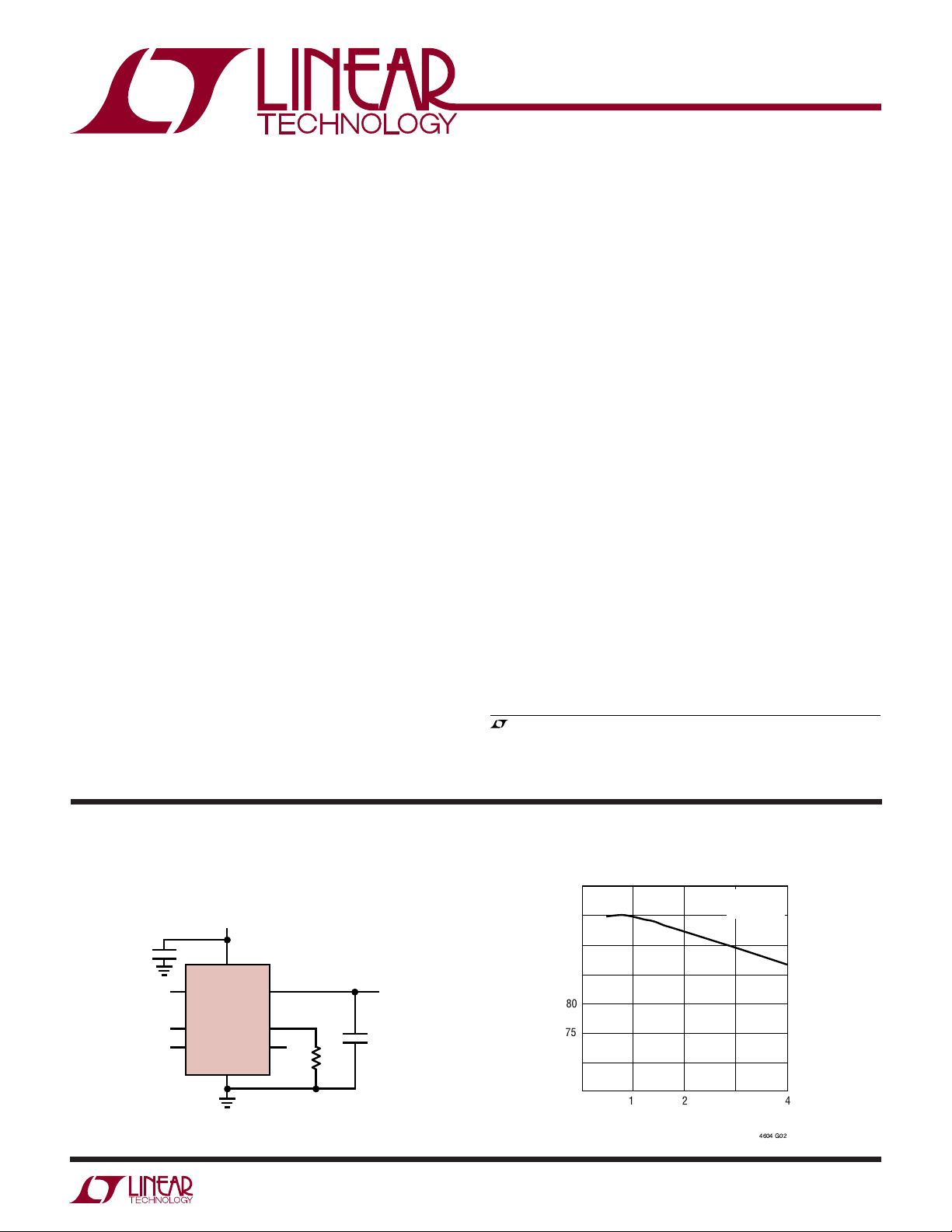
TYPICAL APPLICATION
3.3V to 2.5V/4A μModule Regulator
V
IN
3.3V
10μF
6.3V
PGOOD
LTM4604
COMP
RUN/SS
V
GND
IN
TRACK
V
OUT
FB
V
IN
2.37k
22μF
6.3V
×2
4604 TA01a
V
OUT
2.5V
4A
Effi ciency vs Output Current
100
95
90
85
80
EFFICIENCY (%)
75
70
65
0
VIN = 3.3V
= 2.5V
V
OUT
12 4
OUTPUT CURRENT (A)
3
"$" /
4604f
1
LTM4604
ABSOLUTE MAXIMUM RATINGS
(Note 1)
VIN, PGOOD ................................................. –0.3V to 6V
COMP, RUN/SS, FB, TRACK .........................–0.3V to V
SW, V
........................................–0.3V to (VIN + 0.3V)
OUT
Operating Temperature Range (Note 2) ... –40°C to 85°C
Junction Temperature ........................................... 125°C
Storage Temperature Range ................... –55°C to 125°C
IN
PIN CONFIGURATION
TOP VIEW
TRACK
A
BCDEFG
V
IN
RUN/
SW
GND
66-PIN (15mm ´ 9mm ´ 2.3mm)
= 125°C, θJA = 25°C/W, WEIGHT = 0.86g
SS
GND
LGA PACKAGE
V
OUT
10
11
T
1
2
3
4
5
6
7
8
9
JMAX
PGOOD
COMP
FB
ORDER INFORMATION
LEAD FREE FINISH TRAY PART MARKING* PACKAGE DESCRIPTION TEMPERATURE RANGE
LTM4604EV#PBF
LTM4604IV#PBF
Consult LTC Marketing for parts specifi ed with wider operating temperature ranges. *The temperature grade is identifi ed by a label on the shipping container.
Consult LTC Marketing for information on non-standard lead based fi nish parts.
For more information on lead free part marking, go to: http://www.linear.com/leadfree/
This product is only offered in trays. For more information go to: http://linear.com/packaging/
ELECTRICAL CHARACTERISTICS
The ● denotes the specifi cations which apply over the full operating
temperature range, otherwise specifi cations are at TA = 25°C. VIN = 5V unless otherwise noted. See Figure 15.
SYMBOL PARAMETER CONDITIONS MIN TYP MAX UNITS
V
IN(DC)
V
OUT(DC)
Input Specifi cations
V
IN(UVLO)
I
INRUSH(VIN)
I
Q(VIN NOLOAD)
LTM4604EV#PBF
LTM4604IV#PBF
LTM4604V
LTM4604V
Input DC Voltage
Output Voltage, Total Variation
with Line and Load
Undervoltage Lockout
CIN = 10μF × 1, C
V
= 2.375V to 5.5V, I
IN
V
= 2.375V to 5.5V, I
IN
I
= 0A 1.75 2 2.3 V
OUT
Threshold
Peak Input Inrush Current at
Start-Up
I
= 0A, CIN = 10μF, C
OUT
RUN/SS = 0.01μF, V
V
= 3.3V
IN
V
= 5V
IN
Input Supply Bias Current VIN = 3.3V, V
V
= 3.3V, V
IN
V
= 5V, V
IN
V
= 5V, V
IN
Shutdown, RUN = 0, V
15mm × 9mm × 2.3mm LGA
15mm × 9mm × 2.3mm LGA
= 22μF ×3, RFB = 5.69k 0.5%
OUT
= 1.5V, No Switching
OUT
= 1.5V, Switching Continuous
OUT
= 1.5V, No Switching
OUT
= 1.5V, Switching Continuous
OUT
= 0A to 4A, 0°C ≤ TA ≤ 85°C
OUT
= 0A to 4A
OUT
= 22μF ×3,
OUT
= 1.5V
OUT
= 5V
IN
–40°C to 85°C
–40°C to 85°C
●
2.375 5.5 V
1.478
●
1.470
1.5
1.5
1.522
1.522
0.7
0.7
60
28
100
35
7
μA
mA
μA
mA
μA
4604f
V
V
A
A
2
LTM4604
ELECTRICAL CHARACTERISTICS
The ● denotes the specifi cations which apply over the full operating
temperature range, otherwise specifi cations are at T
SYMBOL PARAMETER CONDITIONS MIN TYP MAX UNITS
I
S(VIN)
Output Specifi cations
I
OUT(DC)
ΔV
OUT(LINE)
V
OUT
ΔV
OUT(LOAD)
V
OUT
V
OUT(AC)
f
S
ΔV
OUT(START)
t
START
ΔV
OUT(LS)
t
SETTLE
I
OUT(PK)
Control Section
V
FB
I
FB
V
RUN
I
TRACK
V
TRACK(OFFSET)
V
TRACK(RANGE)
R
FBHI
PGOOD
ΔV
PGOOD
R
PGOOD
Note 1: Stresses beyond those listed under Absolute Maximum Ratings
may cause permanent damage to the device. Exposure to any Absolute
Maximum Rating condition for extended periods may affect device
reliability and lifetime.
Input Supply Current VIN = 2.5V, V
Output Continuous Current
Range (See Output Current
Derating Curves for Different
V
, V
and TA)
IN
OUT
Line Regulation Accuracy V
Load Regulation Accuracy V
Output Ripple Voltage I
Output Ripple Voltage
Frequency
Turn-On Overshoot C
Turn-on Time C
Peak Deviation for Dynamic
Load Step
Settling Time for Dynamic
Load Step
Output Current Limit C
Voltage at FB Pin I
RUN Pin On/Off Threshold 0.5 0.65 0.8 V
TRACK Pin Current 0.2 μA
Offset Voltage TRACK = 0.4V 30 mV
Tracking Input Range 0 0.8 V
Resistor Between V
OUT
and
FB Pins
PGOOD Range ±7.5 %
PGOOD Resistance Open-Drain Pull-Down 90 150
= 25°C. VIN = 5V unless otherwise noted. See Figure 15.
A
= 1.5V, I
V
= 3.3V, V
IN
V
= 5V, V
IN
= 3.3V, V
V
IN
OUT
OUT
V
IN
V
IN
OUT
V
IN
V
IN
I
OUT
OUT
I
OUT
V
IN
V
IN
OUT
TRACK = V
V
IN
V
IN
OUT
= 1.5V, I
OUT
= 1.5V, I
OUT
= 1.5V 4 A
OUT
= 1.5V, VIN from 2.375V to 5.5V, I
= 1.5V, 0A to 4A
= 3.3V
= 5V
= 0A, C
= 3.3V, V
= 5V, V
= 22μF/X5R/Ceramic ×3
OUT
= 1.5V
OUT
= 1.5V
OUT
= 4A, VIN = 5V, V
= 22μF ×3, V
OUT
= 0A
= 3.3V
= 5V
= 22μF ×3, V
OUT
and RUN/SS = Float
IN
= 3.3V
= 5V
= 4A
OUT
= 4A
OUT
= 4A
OUT
= 0A
OUT
= 1.5V 1.25 MHz
OUT
= 1.5V, RUN/SS = 10nF,
= 1.5V, I
= 1A Resistive Load,
OUT
Load: 0% to 50% to 0% of Full Load,
C
= 22μF ×3 Ceramic
OUT
V
= 5V, V
IN
= 1.5V 25 mV
OUT
Load: 0% to 50% to 0% of Full Load
V
V
V
I
IN
OUT
IN
IN
OUT
OUT
= 5V, V
= 22μF ×3
= 3.3V, V
= 5V, V
= 0A, V
= 0A, V
= 1.5V 10 μs
OUT
= 1.5V
OUT
= 1.5V
OUT
= 1.5V, 0°C ≤ TA ≤ 85°C
OUT
= 1.5V
OUT
Note 2: The LTM4604E is guaranteed to meet performance specifi cations
from 0°C to 85°C. Specifi cations over the –40°C to 85°C operating
temperature range are assured by design, characterization and correlation
with statistical process controls. The LTM4604I is guaranteed over the full
–40°C to 85°C temperature range.
2.9
2.2
1.45
●
●
●
0.1 0.2 %
0.3
0.3
0.6
0.6
10
12
20
20
1.5
1.0
8
8
0.792
●
0.788
0.8
0.8
0.808
0.812
0.2 μA
4.975 4.99 5.025 kΩ
mV
mV
P-P
P-P
mV
mV
ms
ms
A
A
A
%
%
A
A
V
V
Ω
4604f
3
LTM4604
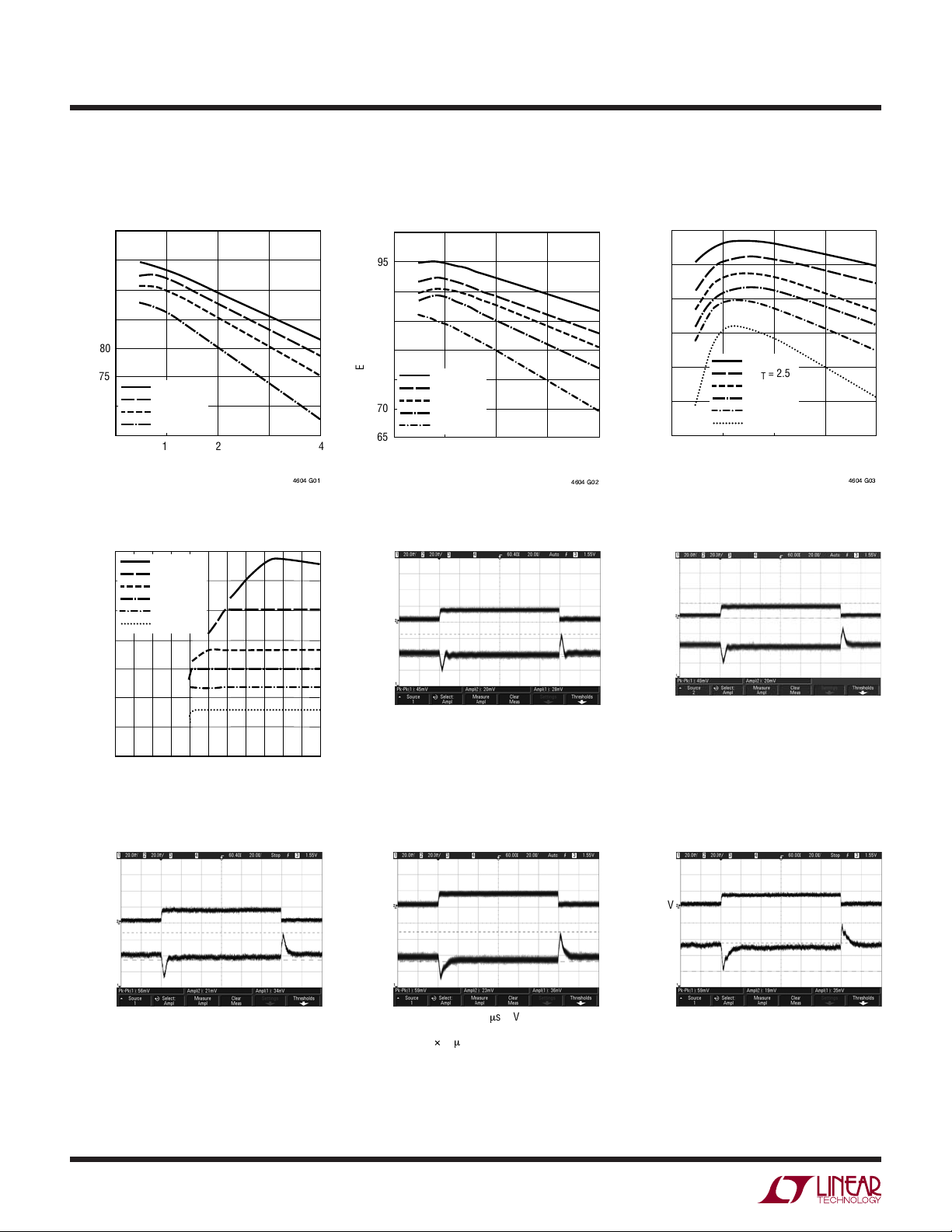
TYPICAL PERFORMANCE CHARACTERISTICS
Effi ciency vs Output Current
V
= 2.5V
IN
100
95
90
85
80
EFFICIENCY (%)
75
70
65
V
= 1.8V
OUT
= 1.5V
V
OUT
= 1.2V
V
OUT
= 0.8V
V
OUT
0
12 4
OUTPUT CURRENT (A)
Minimum Input Voltage
at 4A Load
(V)
OUT
V
3.5
3.0
2.5
2.0
1.5
V
= 3.3V
OUT
= 2.5V
V
OUT
= 1.8V
V
OUT
= 1.5V
V
OUT
= 1.2V
V
OUT
= 0.8V
V
OUT
Effi ciency vs Output Current
VIN = 3.3V
100
95
90
85
80
EFFICIENCY (%)
75
70
3
"$" /
65
V
= 2.5V
OUT
= 1.8V
V
OUT
= 1.5V
V
OUT
= 1.2V
V
OUT
= 0.8V
V
OUT
0
12 4
OUTPUT CURRENT (A)
3
"$" /
Load Transient Response
I
LOAD
2A/DIV
V
OUT
20mV/DIV
Effi ciency vs Output Current
VIN = 5V
95
90
85
80
EFFICIENCY (%)
75
70
65
0
V
V
V
V
V
V
12 34
OUTPUT CURRENT (A)
Load Transient Response
I
LOAD
2A/DIV
V
OUT
20mV/DIV
OUT
OUT
OUT
OUT
OUT
OUT
= 3.3V
= 2.5V
= 1.8V
= 1.5V
= 1.2V
= 0.8V
"$" /!
1.0
0.5
I
LOAD
2A/DIV
V
OUT
20mV/DIV
0
0
0.5
1.5
2.5
34
2
1
VIN (V)
Load Transient Response
= 5V
V
IN
= 1.8V
V
OUT
= 3 × 22μF, 6.3V CERAMICS
C
OUT
20μs/DIV
3.5
4.5
4604 G04
4604 G07
V
= 5V
V
= 5V
IN
= 1.2V
V
OUT
= 4 × 22μF, 6.3V CERAMICS
C
OUT
5.55
20μs/DIV
4604 G05
IN
= 1.5V
V
OUT
= 4 × 22μF, 6.3V CERAMICS
C
OUT
20μs/DIV
4604 G06
Load Transient Response Load Transient Response
I
LOAD
2A/DIV
V
OUT
20mV/DIV
V
= 5V
IN
= 2.5V
V
OUT
= 3 ´ 22mF, 6.3V CERAMICS
C
OUT
20ms/DIV
4604 G08
I
LOAD
2A/DIV
V
OUT
20mV/DIV
V
= 5V
IN
= 3.3V
V
OUT
= 2 × 22μF, 6.3V CERAMICS
C
OUT
20μs/DIV
4604 G09
4604f
4
TYPICAL PERFORMANCE CHARACTERISTICS
Start-Up Start-Up
LTM4604
V
OUT
1V/DIV
I
IN
1A/DIV
= 5V
V
IN
= 2.5V
V
OUT
= 4 × 22μF
C
OUT
NO LOAD
(0.01μF SOFT-START CAPACITOR)
VFB vs Temperature
806
804
802
800
(mV)
FB
V
798
796
794
-50
-25 500 25 10075
Temperature (C)
200μs/DIV
4604 G10
"$" /#
V
OUT
1V/DIV
I
IN
1A/DIV
= 5V
V
IN
= 2.5V
V
OUT
= 4 × 22μF
C
OUT
4A LOAD
(0.01μF SOFT-START CAPACITOR)
Current Limit Foldback
1.6
1.4
1.2
1.0
(V)
0.8
OUT
V
0.6
V
0.2
= 1.5V
OUT
VIN = 5V
= 3.3V
V
IN
= 2.5V
V
0
IN
45 7
3
OUTPUT CURRENT (A)
0.4
200μs/DIV
4604 G11
6
8
4604 G12
Short-Circuit Protection
1.5V Short, No Load
V
OUT
0.5V/DIV
I
IN
4A/DIV
20μs/DIV
4604 G13
Short-Circuit Protection
1.5V Short, 4A Load
V
OUT
0.5V/DIV
I
IN
1A/DIV
100μs/DIV
4604 G14
4604f
5
LTM4604
PIN FUNCTIONS
VIN (B1, C1, C3-C7, D7, E6 and E7): Power Input Pins.
Apply input voltage between these pins and GND pins.
Recommend placing input decoupling capacitance directly
between V
(D8-D11, E8-E11, F6-F11, G6-G11): Power Output
V
OUT
pins and GND pins.
IN
Pins. Apply output load between these pins and GND pins.
Recommend placing output decoupling capacitance directly
between these pins and GND pins. Review Table 4.
GND (G3-G5, F3-F5, E4-E5, A1-A11, B6-B11, C8-C11):
Power Ground Pins for Both Input and Output Returns.
TRACK (E1): Output Voltage Tracking Pin. When the module
is confi gured as a master output, then a soft-start capacitor is placed on the RUN/SS pin to ground to control the
master ramp rate. Slave operation is performed by putting
a resistor divider from the master output to ground, and
connecting the center point of the divider to this pin on
the slave regulator. If tracking is not desired, then connect
the TRACK pin to V
. Load current must be present for
IN
tracking. See Applications Information section.
FB (G2): The Negative Input of the Error Amplifi er. Internally, this pin is connected to V
with a 4.99k precision
OUT
resistor. Different output voltages can be programmed
with an additional resistor between FB and GND pins.
Two power modules can current share when this pin is
connected in parallel with the adjacent module’s FB pin.
See Applications Information section.
COMP (G1): Current Control Threshold and Error Amplifi er
Compensation Point. The current comparator threshold
increases with this control voltage. Two power modules
can current share when this pin is connected in parallel
with the adjacent module’s COMP pin.
PGOOD (F1): Output Voltage Power Good Indicator. Opendrain logic output that is pulled to ground when the output
voltage is not within ±7.5% of the regulation point.
RUN/SS (D1): Run Control and Soft-Start Pin. A voltage
above 0.8V will turn on the module, and below 0.5V will
turn off the module. This pin has a 1M resistor to V
IN
and
a 1000pF capacitor to GND. See Application Infomation
section for soft-start information.
SW (B3 and B4): Switching Node of the circuit is used for
testing purposes. This can be connected to copper on the
board to improve thermal performance. Make sure not to
connect it to other output pins.
TOP VIEW
TRACK
A
BCDEFG
V
SW
GND
IN
RUN/
1
2
3
4
5
6
7
8
9
10
11
PGOOD
COMP
SS
GND
V
OUT
FB
4604f
6

BLOCK DIAGRAM
LTM4604
TRACK
SUPPLY
4.99k
5.76k
PGOOD
RUN/SS
C
SSEXT
TRACK
COMP
C
SS
1000pF
INTERNAL
COMP
R
SS
1M
CONTROL,
DRIVE
FB SW
R
FB
5.76k
10μF
6.3V
×2
M1
M2
L
R1
C2
4.99k
470pF
0.5%
10μF
6.3V
V
IN
V
OUT
GND
4604 BD
10μF
6.3V
22μF
6.3V
×3
V
IN
2.375V TO 5.5V
V
OUT
1.5V
4A
Figure 1. Simplifi ed LTM4604 Block Diagram
DECOUPLING REQUIREMENTS
T
SYMBOL PARAMETER CONDITIONS MIN TYP MAX UNITS
C
IN
C
OUT
External Input Capacitor Requirement
(V
= 2.375V to 5.5V, V
IN
OUT
= 1.5V)
External Output Capacitor Requirement
(V
= 2.375V to 5.5V, V
IN
OUT
= 1.5V)
= 25°C. Use Figure 1 Confi guration.
A
= 4A 10 μF
I
OUT
= 4A 22 100 μF
I
OUT
4604f
7

LTM4604
OPERATION
Power Module Description
The LTM4604 is a standalone non-isolated switch mode
DC/DC power supply. It can deliver up to 4A of DC output
current with few external input and output capacitors.
This module provides a precise regulated output voltage
programmable via one external resistor from 0.8V DC to
5.0V DC over a 2.375V to 5.5V input voltage. A typical
application schematic is shown in Figure 15.
The LTM4604 has an integrated constant frequency current mode regulator with built-in power MOSFETs with
fast switching speed. The typical switching frequency is
1.25MHz. With current mode control and internal feedback
loop compensation, the LTM4604 module has suffi cient
stability margins and good transient performance under a
wide range of operating conditions and with a wide range
of output capacitors, even all ceramic output capacitors.
Current mode control provides cycle-by-cycle fast current
limit. In addition, foldback current limiting is provided
in an overcurrent condition while V
overvoltage and undervoltage comparators pull the open-
drops. Internal
OUT
drain PGOOD output low if the output feedback voltage exits
a ±7.5% window around the regulation point. Furthermore,
in an overvoltage condition, internal top FET M1 is turned
off and bottom FET M2 is turned on and held on until the
overvoltage condition clears.
Pulling the RUN pin below 0.5V forces the controller into its
shutdown state, turning off both M1 and M2. At low load
current, the module works in continuous current mode by
default to achieve minimum output voltage ripple.
The TRACK pin is used for power supply tracking. See the
Applications Information section.
The LTM4604 is internally compensated to be stable over
a wide operating range. Table 4 provides a guideline for
input and output capacitance for several operating conditions. An excel loop analysis tool is provided for transient
and stability analysis.
The FB pin is used to program the output voltage with a
single resistor connected to ground.
8
4604f

APPLICATIONS INFORMATION
LTM4604
A typical LTM4604 application circuit is shown in Figure 15.
External component selection is primarily determined by
the maximum load current and output voltage. Refer to
Table 4 for specifi c external capacitor requirements for a
particular application.
to V
V
IN
There are restrictions in the maximum V
Step-Down Ratios
OUT
and V
IN
OUT
stepdown ratio that can be achieved for a given input voltage.
The LTM4604 is 100% duty cycle, but the V
IN
to V
OUT
minimum dropout is a function of the load current. A typical 0.5V minimum is suffi cient (see Typical Performance
Characteristics).
Output Voltage Programming
The PWM controller has an internal 0.8V reference voltage.
As shown in the Block Diagram, a 4.99k, 0.5% internal
feedback resistor connects the V
and FB pins together.
OUT
The output voltage will default to 0.8V with no feedback
resistor. Adding a resistor R
from the FB pin to GND
FB
programs the output voltage:
kR
499
VV
=+08
OUT
.•
.
Table 1. FB Resistor vs Output Voltage
V
OUT
R
0.8V 1.2V 1.5V 1.8V 2.5V 3.3V
Open 10k 5.76k 4.02k 2.37k 1.62k
FB
FB
R
FB
Input Capacitors
The LTM4604 module should be connected to a low acimpedance DC source. Two 10μF ceramic capacitors are
included inside the module. Additional input capacitors
are only needed if a large load step is required up to a
full 4A level. An input 47μF bulk capacitor is only needed
if the input source impedance is compromised by long
inductive leads or traces.
For a buck converter, the switching duty cycle can be
estimated as:
V
OUT
D
=
V
IN
Without considering the inductor current ripple, the RMS
current of the input capacitor can be estimated as:
I
OUT MAX
()
%
η
DD
••–=
1
()
I
CIN RMS
()
In the above equation, η% is the estimated effi ciency of
the power module. The bulk capacitor can be a switcherrated electrolytic aluminum capacitor, OS-CON capacitor
for bulk input capacitance due to high inductance traces
or leads. If a low inductance plane is used to power the
device, then no input capacitance is required. The two
internal 10μF ceramics are typically rated for 2A to 3A of
RMS ripple current. The worst-case ripple current for the
4A maximum current is 2A or less.
Output Capacitors
The LTM4604 is designed for low output voltage ripple.
The bulk output capacitors defi ned as C
are chosen
OUT
with low enough effective series resistance (ESR) to meet
the output voltage ripple and transient requirements. C
OUT
can be a low ESR tantalum capacitor, a low ESR polymer
capacitor or an X5R/X7R ceramic capacitor. The typical
output capacitance range is 22μF to 100μF. Additional
output fi ltering may be required by the system designer
if further reduction of output ripple or dynamic transient
spike is required. Table 4 shows a matrix of different
output voltages and output capacitors to minimize the
voltage droop and overshoot during a 2A/μs transient.
The table optimizes the total equivalent ESR and total
bulk capacitance to maximize transient performance. The
Linear Technology μModule Power Design Tool can be for
further optimization.
Fault Conditions: Current Limit and Overcurrent
Foldback
The LTM4604 has current mode control, which inherently limits the cycle-by-cycle inductor current not only
in steady-state operation, but also in transient.
To further limit current in the event of an overload condition, the LTM4604 provides foldback current limiting as
the output voltage falls. The LTM4604 device has overtemperature shutdown protection that inhibits switching
operation around 150°C.
4604f
9

LTM4604
APPLICATIONS INFORMATION
Run Enable and Soft-Start
The RUN/SS pin provides dual functions of enable and
soft-start control. The RUN/SS pin is used to control
turn on of the LTM4604. While this pin is below 0.5V, the
LTM4604 will be in a 7μA low quiescent current state. A
0.8V threshold will enable the LTM4604. This pin can be
used to sequence LTM4604 devices. The soft-start control
is provided by a 1M pull-up resistor (R
capacitor (C
) as drawn in the Block Diagram. An external
SS
capacitor can be applied to the RUN/SS pin to increase the
soft-start time. A typical value is 0.01μF. The approximate
equation for soft-start is:
t
SOFTSTART
⎛
=
V
⎜
VV
–.•18
⎝
IN
⎞
IN
⎟
⎠
where RSS and CSS are shown in the Block Diagram of
Figure 1, 1.8V is the soft-start upper range, and C
is the additional capacitance for further soft-start contol.
The soft-start function can also be used to control the
output ramp-up time, so that another regulator can be
easily tracked. An independent ramp control signal can
be applied to the master ramp, otherwise, connect the
TRACK pin to V
to disable tracking.
IN
) and a 1000pF
SS
RC C
SS SS SSE
+ln
()
XXT
SSEXT
X5R OR X7R
C
SSEXT
X5R OR X7R
C
IN1
10μF
6.3V
C
IN2
10μF
6.3V
PGOOD
LTM4604
COMP
RUN/SS
PGOOD
LTM4604
COMP
RUN/SS
V
5V
V
GND
V
5V
V
GND
IN
IN
TRACK
IN
IN
TRACK
V
MASTER
4604 F02
3.3V
4A
V
SLAVE
1.5V
4A
V
OUT
C
OUT1
FB3
FB
22μF
6.3V ×3
X5R OR
X7R
C
OUT2
22μF
6.3V ×3
X5R OR
X7R
FB
RAMP
CONTROL
OR V
V
OUT
FB
R
FB2
5.76k
R
IN
1.62k
R
5.76k
R
FB1
4.99k
Output Voltage Tracking
Output voltage tracking can be programmed externally
using the TRACK pin. The output can be tracked up and
down with another regulator. The master regulator’s
output is divided down with an external resistor divider
that is the same as the slave regulator’s feedback divider
to implement coincident tracking. The LTM4604 uses a
very accurate 4.99k resistor for the top feedback resistor.
Figure 2 shows an example of coincident tracking.
R
2
V
TRACK
=
V
V
is the track ramp applied to the slave’s TRACK pin.
TRACK
applies the track reference for the slave output up
TRACK
to the point of the programmed value at which V
proceeds beyond the 0.8V reference value. The V
499.
FB
kR
+
FB
2
V
•
MASTER
TRACK
TRACK
pin must go beyond 0.8V to ensure the slave output has
reached its fi nal value. Load current must be present for
proper tracking.
OUTPUT VOLTAGE (V)
Figure 2
TIME
Figure 3
MASTER OUTPUT
SLAVE OUTPUT
4604 F03
4604f
10

APPLICATIONS INFORMATION
LTM4604
Ratio metric modes of tracking can be achieved by selecting
different resistor values to change the output tracking ratio.
The master output must be greater than the slave output
for the tracking to work. Linear Technology Tracker Cad26
can be used to implement different tracking scenarios. The
Master and Slave data inputs can be used to implement
the correct resistor values for coincident or ratio tracking.
The master and slave regulators require load current for
tracking down.
Power Good
The PGOOD pin is an open-drain pin that can be used to
monitor valid output voltage regulation. This pin monitors
a ±7.5% window around the regulation point.
COMP Pin
The pin is the external compensation pin. The module
has already been internally compensated for all output
voltages. Table 4 is provided for most application requirements. A spice model will be provided for other control
loop optimizations.
Parallel Operation
The LTM4604 device is an inherently current mode controlled device. Parallel modules will have very good current
sharing. This will balance the thermals on the design.
Figure 16 shows a schematic of the parallel design. The
voltage feedback changes with the variable N as more
modules are paralleled. The equation:
k
499
VV
=+08
OUT
.•
.
R
N
FB
R
FB
N is the number of paralleled modules.
Thermal Considerations and Output Current Derating
The power loss curves in Figures 4 and 5 can be used
in coordination with the load derating curves in Figures
6 through 13 for calculating an approximate θ
for the
JA
module with and without heat sinking methods with various airfl ow conditions. Thermal models are derived from
several temperature measurements at the bench, and are
correlated with thermal analysis software. Tables 2 and
3 provide a summary of the equivalent θ
conditions. These equivalent θ
parameters are correlated
JA
for the noted
JA
to the measured values and improve with air fl ow. The
maximum junction temperature is monitored while the
derating curves are derived.
2.0
1.8
1.6
1.4
1.2
1.0
WATTS
0.8
0.6
0.4
0.2
0
2.0
1.8
1.6
1.4
1.2
1.0
WATTS
0.8
0.6
0.4
0.2
0
0
234
1
LOAD CURRENT (A)
0
12
LOAD CURRENT (A)
5V TO 1.2V
POWER LOSS
3.3V TO 1.2V
POWER LOSS
34
4604 F04
5
Figure 4. 1.2V Power Loss Figure 5. 2.5V Power Loss
5V TO 2.5V
POWER LOSS
3.3V TO 2.5V
POWER LOSS
5
4604 F05
4604f
11

LTM4604
APPLICATIONS INFORMATION
4.0
3.5
3.0
2.5
4.0
3.5
3.0
2.5
2.0
1.5
LOAD CURRENT (A)
1.0
0.5
0LFM
200LFM
400LFM
0
75 115
70
80
85
AMBIENT TEMPERATURE (°C)
Figure 6. 5VIN to 1.2V
4.0
3.5
3.0
2.5
2.0
1.5
LOAD CURRENT (A)
1.0
0.5
0LFM
200LFM
400LFM
0
75 115
70
80
85
AMBIENT TEMPERATURE (°C)
2.0
1.5
LOAD CURRENT (A)
1.0
0.5
90
95
No Heat Sink Figure 7. 5VIN to 1.2V
OUT
90
95
100
100
105
105
110
110
4606 F08
4606 F06
4.0
3.5
3.0
2.5
2.0
1.5
LOAD CURRENT (A)
1.0
0.5
0LFM
200LFM
400LFM
0
75 115
70
AMBIENT TEMPERATURE (°C)
0LFM
200LFM
400LFM
0
75 115
70
AMBIENT TEMPERATURE (°C)
90
80
80
95
85
85
100
with Heat Sink
OUT
90
95
100
105
105
110
4606 F07
110
4606 F09
12
Figure 8. 3.3VIN to 1.2V
4.0
3.5
3.0
2.5
2.0
1.5
LOAD CURRENT (A)
1.0
0.5
0LFM
200LFM
400LFM
0
75
70
80
85
AMBIENT TEMPERATURE (°C)
Figure 10. 5VIN to 2.5V
No Heat Sink Figure 9. 3.3VIN to 1.2V
OUT
4.0
3.5
3.0
2.5
2.0
1.5
LOAD CURRENT (A)
1.0
0.5
90
95
100
No Heat Sink Figure 11. 5VIN to 2.5V
OUT
105
110
4606 F10
0
70
with Heat Sink
OUT
0LFM
200LFM
400LFM
90
75 115
80
AMBIENT TEMPERATURE (°C)
95
85
OUT
110
100
105
4606 F11
with Heat Sink
4604f

APPLICATIONS INFORMATION
4.0
3.5
3.0
2.5
LTM4604
4.0
3.5
3.0
2.5
2.0
1.5
LOAD CURRENT (A)
1.0
0.5
0LFM
200LFM
400LFM
0
75 115
70
AMBIENT TEMPERATURE (°C)
90
80
85
Figure 12. 3.3VIN to 2.5V
2.0
1.5
LOAD CURRENT (A)
1.0
0.5
95
OUT
110
100
105
4606 F12
No Heat Sink Figure 13. 3.3VIN to 2.5V
0LFM
200LFM
400LFM
0
75 115
70
AMBIENT TEMPERATURE (°C)
90
80
95
85
OUT
110
100
105
4606 F13
with Heat Sink
4604f
13

LTM4604
APPLICATIONS INFORMATION
Table 2. 1.2V Output
DERATING CURVE VIN (V) POWER LOSS CURVE AIR FLOW (LFM) HEAT SINK θJA (°C/W)
Figures 6, 8 3.3, 5 Figure 4 0 None 25
Figures 6, 8 3.3, 5 Figure 4 200 None 22.5
Figures 6, 8 3.3, 5 Figure 4 400 None 21
Figures 7, 9 3.3, 5 Figure 4 0 BGA Heat Sink 21
Figures 7, 9 3.3, 5 Figure 4 200 BGA Heat Sink 20
Figures 7, 9 3.3, 5 Figure 4 400 BGA Heat Sink 18
Table 3. 2.5V Output
DERATING CURVE VIN (V) POWER LOSS CURVE AIR FLOW (LFM) HEAT SINK θJA (°C/W)
Figures 10, 12 3.3, 5 Figure 5 0 None 25
Figures 10, 12 3.3, 5 Figure 5 200 None 21
Figures 10, 12 3.3, 5 Figure 5 400 None 21
Figures 11, 13 3.3, 5 Figure 5 0 BGA Heat Sink 21
Figures 11, 13 3.3, 5 Figure 5 200 BGA Heat Sink 18
Figures 11, 13 3.3, 5 Figure 5 400 BGA Heat Sink 16
Table 4. Output Voltage Response Versus Component Matrix (Refer to Figure 17), 0A to 2A Load Step Typical Measured Values
C
V
(V)
OUT
1.2 10μF 56μF Aluminum 100μF 6.3V None 2.5 21 43 10 2 10
1.2 10μF 56μF Aluminum 22μF ×4 None 3.3 23 45 10 2 10
1.2 10μF 56μF Aluminum 22μF ×4 None 5 24 46 10 2 10
1.5 10μF 56μF Aluminum 100μF 6.3V None 2.5 19 41 10 2 5.76
1.5 10μF 56μF Aluminum 22μF ×4 None 3.3 21 43 10 2 5.76
1.5 10μF 56μF Aluminum 22μF ×4 None 5 21 43 10 2 5.76
1.8 10μF 56μF Aluminum 100μF 6.3V None 2.5 25 50 10 2 4.02
1.8 10μF 56μF Aluminum 22μF ×3 None 3.3 30 60 10 2 4.02
1.8 10μF 56μF Aluminum 22μF ×3 None 5 30 60 10 2 4.02
2.5 10μF 56μF Aluminum 100μF 6.3V None 2.5 22 45 12 2 2.37
2.5 10μF 56μF Aluminum 22μF ×3 None 3.3 25 55 12 2 2.37
2.5 10μF 56μF Aluminum 22μF ×3 None 5 25 55 12 2 2.37
3.3 10μF 56μF Aluminum 100μF 6.3V None 2.5 22 50 15 2 1.62
3.3 10μF 56μF Aluminum 22μF ×3 None 3.3 25 56 15 2 1.62
3.3 10μF 56μF Aluminum 22μF ×3 None 5 25 56 15 2 1.62
IN
(CERAMIC) CIN (Bulk)
C
OUT
(CERAMIC) C
COMP
VIN (V)
DROOP
(mV)
PEAK-TOPEAK(mV)
RECOVERY
(μs)
LOAD STEP
(A/μs)
R
FB
(kΩ)
14
4604f

APPLICATIONS INFORMATION
LTM4604
Safety Considerations
The LTM4604 modules do not provide isolation from V
. There is no internal fuse. If required, a slow blow fuse
V
OUT
IN
to
with a rating twice the maximum input current needs to be
provided to protect each unit from catastrophic failure.
Layout Checklist/Example
The high integration of LTM4604 makes the PCB board
layout very simple and easy. However, to optimize its electrical and thermal performance, some layout considerations
are still necessary.
• Use large PCB copper areas for high current path,
including V
, GND and V
IN
. It helps to minimize the
OUT
PCB conduction loss and thermal stress.
• Place high frequency ceramic input and output capacitors
next to the V
, GND and V
IN
pins to minimize high
OUT
frequency noise.
• Place a dedicated power ground layer underneath the
unit.
• To minimize the via conduction loss and reduce module
thermal stress, use multiple vias for interconnection
between top layer and other power layers.
• Do not put vias directly on the pads unless they are
capped.
• SW pads can be soldered to board to improve thermal
performance.
Figure14 gives a good example of the recommended
layout.
GND
•
•• ••••
•
V
IN
••
•
•
•••••••••••••••••••••
C
IN
Figure 14. Recommended PCB Layout
V
OUT
C
OUT
C
OUT
C
OUT
••
••
••••
••
SW
••
•
••
••
•••
•••
••••
•••
•••
GND
•
4604 F14
V
IN
2.375V TO 5.5V
C
IN
10μF
6.3V
X5R OR X7R
V
OPEN-DRAIN
PULL UP
C
SSEXT
0.01μF
PGOOD
LTM4604
COMP
RUN/SS
GND
IN
TRACK
V
OUT
FB
R
FB
5.69k
0.5%
4604 F15
V
OUT
1.5V
4A
C
OUT
22μF ×3
6.3V
X5R OR X7R
REFER TO
TABLE 4
Figure 15. Typical 2.375V to 5.5V Input, 1.5V at 4A Design
4604f
15

LTM4604
TYPICAL APPLICATIONS
OPEN-DRAIN PULL UP
10μF
X5R OR X7R
C
SSEXT
0.01μF
10μF
X5R OR X7R
C
6.3V
C
6.3V
IN1
IN2
V
IN
2.375V TO 5V
V
IN
PGOOD
LTM4604
COMP
RUN/SS
GND
V
IN
PGOOD
LTM4604
COMP
RUN/SS
GND
V
OUT
TRACK
V
OUT
TRACK
V
= 0.8V × ((4.99k/N) + RFB)/R
OUT
WHERE N IS THE NUMBER OF PARALLEL DEVICES
C
OUT1
4604 F16
22μF ×3
6.3V
X5R OR X7R
REFER TO
TABLE 4
C
OUT2
22μF ×3
6.3V
X5R OR X7R
REFER TO
TABLE 4
FB
R
FB
2.87k
FB
FB
V
OUT
1.5V
8A
Figure 16. Two LTM4604s in Parallel, 1.5V at 8A Design
4604f
16

TYPICAL APPLICATIONS
OPEN-DRAIN
PULL UP
V
IN
3.3V TO 5V
C
IN
50k
10μF
6.3V
X5R OR X7R
V
IN
C
SSEXT
0.01μF
PGOOD
COMP
RUN/SS
LTM4604
TRACK
GND
V
OUT
FB
R
FB
2.37k
C
OUT
22μF ×3
6.3V
X5R OR X7R
REFER TO
TABLE 4
4604 F17
Figure 17. 3.3V to 5V Input, 2.5V at 4A Design
V
OUT
2.5V
4A
LTM4604
4604f
17

LTM4604
PACKAGE DESCRIPTION
12.70
BSC
0.864 – 0.914
FGE
D
0.864 – 0.914
BSC
7.620
SUBSTRATE
CAP
MOLD
C
0.29 – 0.35
Z
B
1.27
DETAIL A
bbb Z
BSC
A
PADS
PAD 1
56
711 910
PACKAGE BOTTOM VIEW
82143
3
SEE NOTES
Module
m
LTMXXXXXX
PIN “A1”
COMPONENT
LGA 66 0607 REV A
PACKAGE IN TRAY LOADING ORIENTATION
BEVEL
TRAY PIN 1
LGA Package
66-Lead (15mm × 9mm × 2.32mm)
(Reference LTC DWG # 05-08-1807 Rev A)
15.00
aaa Z
2.19 – 2.45
Y
X
BSC
9.00
BSC
1.90 – 2.10
PAD “A1”
4
CORNER
DETAIL A
PACKAGE SIDE VIEW
aaa Z
PACKAGE TOP VIEW
0.15
0.10
TOLERANCE
DETAILS OF PAD #1 IDENTIFIER ARE OPTIONAL,
BUT MUST BE LOCATED WITHIN THE ZONE INDICATED.
THE PAD #1 IDENTIFIER MAY BE EITHER A MOLD OR A
MARKED FEATURE
4
3
NOTES:
1. DIMENSIONING AND TOLERANCING PER ASME Y14.5M-1994
2. ALL DIMENSIONS ARE IN MILLIMETERS
LAND DESIGNATION PER JESD MO-222
6.350
5.080
3.810
2.540
1.270
0.4445
0.000
0.4445
1.270
2.540
3.810
5.080
6.350
3.810
2.540
1.270
aaa
bbb
SYMBOL
5. PRIMARY DATUM -Z- IS SEATING PLANE
6. THE TOTAL NUMBER OF PADS: 66
2.540
1.270
0.000
0.4445
0.4445
TOP VIEW
SUGGESTED PCB LAYOUT
3.810
4604f
18

PACKAGE DESCRIPTION
PIN NAME PIN NAME PIN NAME PIN NAME PIN NAME PIN NAME PIN NAME
A1 GND B1 V
A2 GND B2 – C2 – D2 – E2 – F2 – G2 FB
A3 GND B3 SW C3 V
A4 GND B4 SW C4 V
A5 GND B5 – C5 V
A6 GND B6 GND C6 V
A7 GND B7 GND C7 V
A8 GND B8 GND C8 GND D8 V
A9 GND B9 GND C9 GND D9 V
A10 GND B10 GND C10 GND D10 V
A11 GND B11 GND C11 GND D11 V
IN
Pin Assignment Table
(Arranged by Pin Number)
C1 V
D1 RUN/SS E1 TRACK F1 PGOOD G1 COMP
IN
D3 – E3 – F3 GND G3 GND
IN
D4 – E4 GND F4 GND G4 GND
IN
D5 – E5 GND F5 GND G5 GND
IN
D6 – E6 V
IN
D7 V
IN
IN
OUT
OUT
OUT
OUT
E7 V
E8 V
E9 V
E10 V
E11 V
IN
IN
OUT
OUT
OUT
OUT
F6 V
F7 V
F8 V
F9 V
F10 V
F11 V
OUT
OUT
OUT
OUT
OUT
OUT
G6 V
G7 V
G8 V
G9 V
G10 V
G11 V
LTM4604
OUT
OUT
OUT
OUT
OUT
OUT
Information furnished by Linear Technology Corporation is believed to be accurate and reliable.
However, no responsibility is assumed for its use. Linear Technology Corporation makes no representation that the interconnection of its circuits as described herein will not infringe on existing patent rights.
4604f
19

LTM4604
RELATED PARTS
PART NUMBER DESCRIPTION COMMENTS
LTC2900 Quad Supply Monitor with Adjustable Reset Timer Monitors Four Supplies; Adjustable Reset Timer
LTC2923 Power Supply Tracking Controller Tracks Both Up and Down; Power Supply Sequencing
LTM4600 10A DC/DC μModule Basic 10A DC/DC μModule
LTM4601 12A DC/DC μModule with PLL, Output Tracking/
Margining and Remote Sensing
LTM4602 6A DC/DC μModule Pin Compatible with the LTM4600
LTM4603 6A DC/DC μModule with PLL and Output Tracking/
Margining and Remote Sensing
LTM4608 8A Low Voltage μModule 2.375V ≤ V
Synchronizable, PolyPhase Operation, LTM4601-1 Version has no Remote
Sensing
Synchronizable, PolyPhase Operation, LTM4603-1 Version has no Remote
Sensing, Pin Compatible with the LTM4601
≤ 5V, Parallel for Higher Output Current, 9mm × 15mm × 2.8mm
IN
20
Linear Technology Corporation
1630 McCarthy Blvd., Milpitas, CA 95035-7417
(408) 432-1900 ● FAX: (408) 434-0507
●
www.linear.com
4604f
LT 0807 • PRINTED IN USA
© LINEAR TECHNOLOGY CORPORATION 2007
 Loading...