

FEATURES
Electrical Specifications Subject to Change
LTM4600
10A High Effi ciency
DC/DC µModule
U
DESCRIPTIO
■
Complete Switch Mode Power Supply
■
Wide Input Voltage Range: 4.5V to 20V
■
10A DC, 14A Peak Output Current
■
Parallel Two µModules™ for 20A Output Current
■
0.6V to 5V Output Voltage
■
1.5% Regulation
■
Ultrafast Transient Response
■
Current Mode Control
■
Pb-Free (e4) RoHS Compliant Package
■
Up to 92% Effi ciency
■
Programmable Soft-Start
■
Output Overvoltage Protection
■
Optional Short-Circuit Shutdown Timer
■
Small Footprint, Low Profi le (15mm × 15mm ×
2.8mm) Surface Mount LGA Package
U
APPLICATIO S
■
Telecom and Networking Equipment
■
Servers
■
Industrial Equipment
■
Point of Load Regulation
■
Other General Purpose Step Down DC/DC
, LTC, LT and LTM are registered trademarks of Linear Technology Corporation.
µModule is a trademark of Linear Technology Corporation. All other trademarks are the
property of their respective owners. Protected by U.S. Patents including 5481178,
6100678, 6580258, 5847554, 6304066.
The LTM®4600 is a complete 10A, DC/DC step down power
supply. Included in the package are the switching controller, power FETs, inductor, and all support components.
Operating over an input voltage range of 4.5V to 20V, the
LTM4600 supports an output voltage range of 0.6V to 5V,
set by a single resistor. This high effi ciency design delivers
10A continuous current (14A peak), needing no heat sinks
or airfl ow to meet power specifi cations. Only bulk input
and output capacitors are needed to fi nish the design.
The low profi le package (2.8mm) enables utilization of
unused space on the bottom of PC boards for high density
point of load regulation. High switching frequency and an
adaptive on-time current mode architecture enables a very
fast transient response to line and load changes without
sacrifi cing stability. Fault protection features include
integrated overvoltage and short circuit protection with
a defeatable shutdown timer. A built-in soft-start timer is
adjustable with a small capacitor.
The LTM4600 is packaged in a thermally enhanced, compact
(15mm × 15mm) and low profi le (2.8mm) over-molded
Land Grid Array (LGA) package suitable for automated
assembly by standard surface mount equipment. The
LTM4600 is Pb-free and RoHS certifi ed.
U
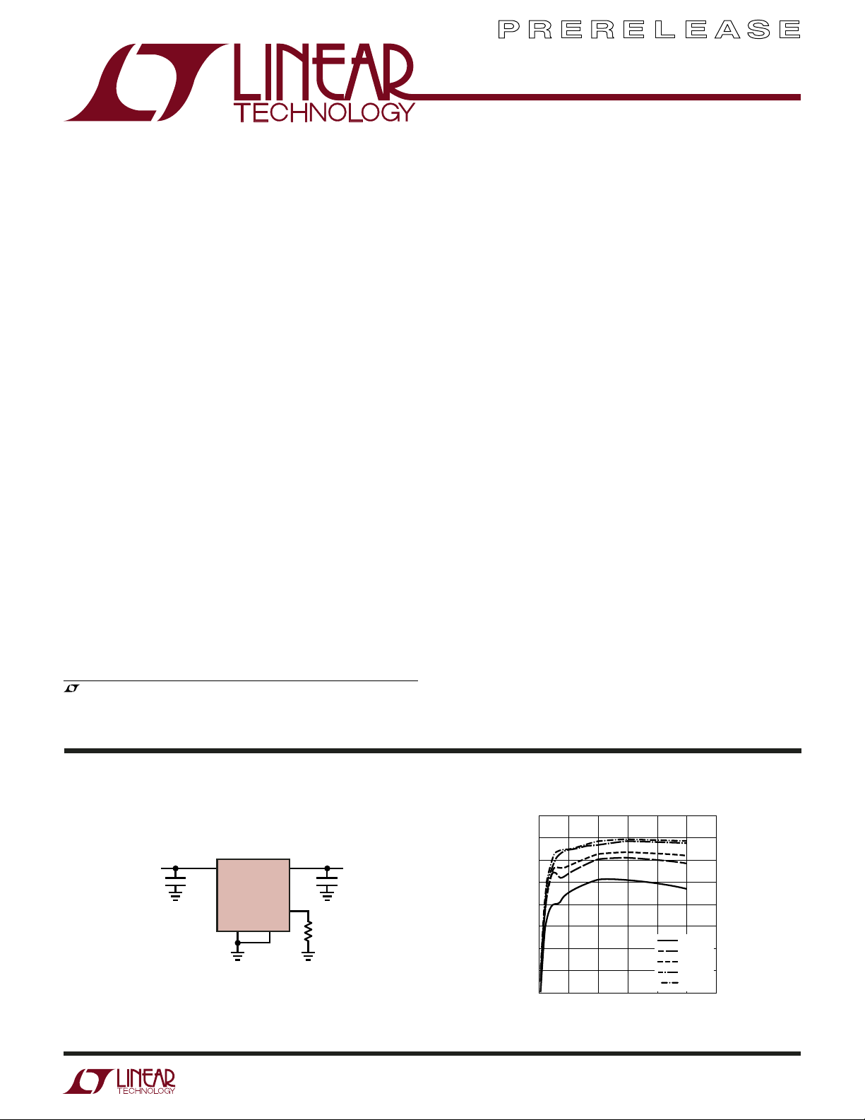
TYPICAL APPLICATIO
10A µModule Power Supply with 4.5V to 20V Input
V
4.5V TO 20V
IN
V
C
IN
V
IN
LTM4600
V
OSET
PGND SGND
OUT
C
OUT
66.5k
4600 TA01a
V
OUT
1.5V
10A
PRERELEASE
Effi ciency vs Load Current
100
90
80
70
60
50
EFFICIENCY (%)
40
30
20
0
with 12V
24 8
LOAD CURRENT (A)
(FCB = 0)
IN
6
0.6V
1.2V
1.5V
2.5V
3.3V
10
OUT
OUT
OUT
OUT
OUT
4600 TA01b
12
4600p
1
LTM4600
WW
W
ABSOLUTE AXI U RATI GS
U
UUW
PACKAGE/ORDER I FOR ATIO
(Note 1)
FCB, EXTVCC, PGOOD, RUN/SS, V
, SVIN, F
V
IN
, COMP ............................................. –0.3V to 2.7V
V
OSET
........................................... –0.3V to 20V
ADJ
.......... –0.3V to 6V
OUT
Operating Temperature Range (Note 2) ... –40°C to 85°C
Junction Temperature ........................................... 125°C
Storage Temperature Range ................... –65°C to 150°C
V
PGND
TOP VIEW
IN
ADJ
F
IN
OSET
EXTVCCV
SV
COMP
SGND
RUN/SS
FCB
PGOOD
ORDER PART
NUMBER
LTM4600EV
LTM4600IV
LGA PART
MARKING
V
OUT
104-LEAD (15mm × 15mm × 2.8mm)
Consult LTC Marketing for parts specifi ed with wider operating temperature ranges.
The ● denotes the specifi cations which apply over the –40°C to 85°C
ELECTRICAL CHARACTERISTICS
temperature range, otherwise specifi cations are at TA = 25°C, VIN = 12V. External CIN = 120µF, C
LGA PACKAGE
T
= 125°C, θJA = 15°C/W
JMAX
= 200µF/Ceramic per typical
OUT
application (front page) confi guration.
SYMBOL PARAMETER CONDITIONS MIN TYP MAX UNITS
V
IN(DC)
V
OUT(DC)
Input Specifi cations
V
IN(UVLO)
I
INRUSH(VIN)
I
Q(VIN)
I
S(VIN)
Input DC Voltage
Output Voltage
V
= 12V, V
IN
V
= 12V, V
IN
V
= 5V, V
IN
Under Voltage Lockout Threshold I
Input Inrush Current at Startup
V
= 5V
IN
V
= 12V
IN
Input Supply Bias Current
V
= 12V, V
IN
V
= 12V, V
IN
VIN = 5V, V
V
= 5V, V
IN
Shutdown, RUN = 0, V
Input Supply Current
V
= 12V, V
IN
V
= 12V, V
IN
V
= 5V, V
IN
= 1.5V, I
OUT
= 1.5V, I
OUT
= 1.5V, I
OUT
= 1.5V, FCB = 5V
OUT
= 1.5V, FCB = 0V
OUT
= 1.5V, FCB = 5V
OUT
= 1.5V, FCB = 0V
OUT
IN
= 1.5V, I
OUT
= 3.3V, I
OUT
= 1.5V, I
OUT
OUT
OUT
= 0A
OUT
= 12V
OUT
OUT
= 10A
OUT
= 0A
= 0A
= 10A
= 10A
FCB = 0
= 0A 3.4 4 V
OUT
= 0A. V
I
OUT
I
= 0A, EXTVCC Open
OUT
= 1.5V, FCB = 0
OUT
●
4.5 20 V
●
1.478 1.50 1.522 V
1.52
3.13
3.64
0.6
0.7
1.2
42
1.0
52
15
LTM4600EV
LTM4600IV
mA
mA
mA
mA
A
A
µA
A
A
A
2
4600p
PRERELEASE
LTM4600
The ● denotes the specifi cations which apply over the –40°C to 85°C
ELECTRICAL CHARACTERISTICS
temperature range, otherwise specifi cations are at T
SYMBOL PARAMETER CONDITIONS MIN TYP MAX UNITS
Output Specifi cations
I
OUTDC
ΔV
/ΔVIN Line Regulation Accuracy
OUT
/ΔI
ΔV
OUT
OUT
V
OUT(AC)
Fs Output Ripple Voltage Frequency FCB = 0V, I
t
START
ΔV
OUTLS
t
SETTLE
I
OUTPK
Control Stage
V
OSET
V
RUN/SS
I
RUN(C)/SS
I
RUN(D)/SS
– SV
V
IN
IN
I
EXTVCC
R
FBHI
V
FCB
I
FCB
PGOOD Output
ΔV
OSETH
ΔV
OSETL
ΔV
OSET(HYS)
V
PGL
Note 1: Absolute Maximum Ratings are those values beyond which the life
of a device may be impaired.
Note 2: The LTM4600E is guaranteed to meet performance specifi cations
from 0°C to 85°C. Specifi cations over the –40°C to 85°C operating
Output Continuous Current Range
(See Output Current Derating Curves for
Different V
I
OUT
IN
= 0A
, V
OUT
and TA)
Load Regulation Accuracy
V
= 5V
IN
V
= 12V
IN
Output Ripple Voltage
V
IN
V
IN
= 12V, V
= 5V, V
= 1.5V, FCB = 0V
OUT
= 1.5V, FCB = 0V
OUT
Turn-On Time
V
= 12V
IN
V
= 5V
IN
Voltage Drop for Dynamic Load Step
V
= 12V, V
IN
OUT
= 1.5V
Settling Time for Dynamic Load Step
V
= 12V
IN
Output Current Limit
V
= 12V, V
IN
V
= 5V, V
IN
Voltage at V
= 1.5V
OUT
= 1.5V
OUT
Pin I
OSET
RUN ON/OFF Threshold 0.8 1.5 2 V
Soft-Start Charging Current V
Soft-Start Discharging Current V
Current into EXTVCC Pin FCB = 0V, V
Resistor Between V
and FB Pins 100 kΩ
OUT
Forced Continuous Threshold 0.57 0.6 0.63 V
Forced Continuous Pin Current V
PGOOD Upper Threshold V
PGOOD Lower Threshold V
PGOOD Hysteresis V
PGOOD Low Voltage I
= 25°C, VIN = 12V. Per typical application (front page) confi guration.
A
= 12V, V
V
IN
= 1.5V. FCB = 0V
V
OUT
= 1.5V. FCB = 0V
V
OUT
0A to 10A
= 0A
I
OUT
= 1.5V 0 10 A
OUT
● 0.3 %
±1
●
±1
15
20 25
800 kHz
= 5A, VIN = 12V, V
OUT
OUT
●
=
1.5V
V
OUT
= 1.5V, I
OUT
= 10A
0.5
0.7
Load Step: 0A to 5A/µs
C
= 3 • 22µF 6.3V, 470µF 4V Pos Cap,
OUT
36 mV
See Table 2
Load: 10% to 90% to 10% of Full Load 25 µs
17
17
= 0A, V
OUT
RUN/SS
RUN/SS
= 1.5V
OUT
= 0V –0.5 –1.2 –3 µA
= 4V 0.8 1.8 3 µA
●
0.594 0.6 0.606 V
EXTVCC = 0, FCB = 0V 100 mV
= 1.5V, I
OUT
= 0.6V –1 –2 µA
FCB
Rising 7.5 10 12.5 %
OSET
Falling –7.5 –10 –12.5 %
OSET
Returning 1 2.5 %
OSET
= 5mA 0.15 0.4 V
PGOOD
= 0A 16 mA
OUT
temperature range are assured by design, characterization and correlation
with statistical process controls. The LTM4600I is guaranteed and tested
over the –40°C to 85°C temperature range.
mV
mV
P-P
P-P
ms
ms
%
%
A
A
PRERELEASE
4600p
3
LTM4600
w
)
(
)
(
)
(
)
UW
TYPICAL PERFOR A CE CHARACTERISTICS
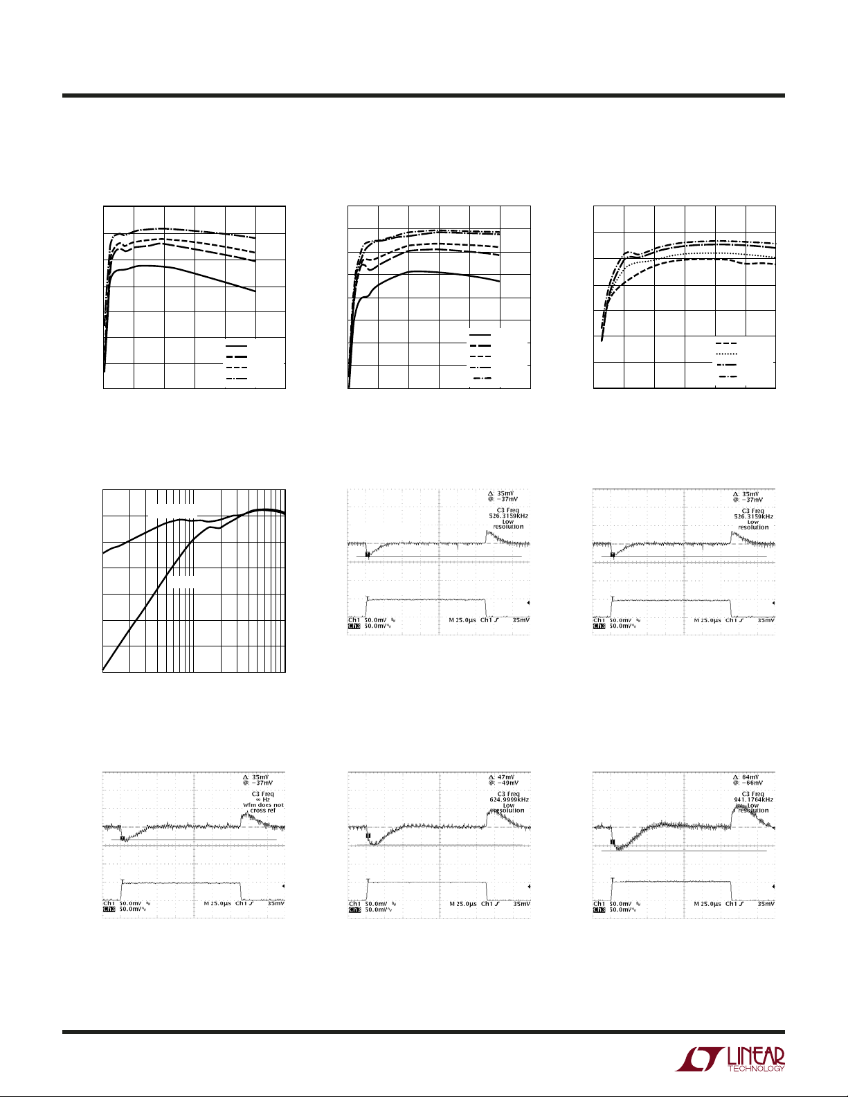
Effi ciency vs Load Current
ith 5V
100
90
80
70
60
EFFICIENCY (%)
50
40
30
0
(FCB = 0)
IN
24
LOAD CURRENT (A)
Effi ciency vs Load Current
with Different FCB Settings
90
80
70
60
50
EFFICIENCY (%)
40
30
20
0.1
FCB > 0.7V
FCB = GND
LOAD CURRENT (A)
0.6V
OUT
1.2V
OUT
1.5V
OUT
2.5V
OUT
812
610
4600 G01
1
10
4600 G04
Effi ciency vs Load Current
with 12V(FCB = 0
100
90
80
70
60
50
EFFICIENCY (%)
40
30
20
24 8
0
LOAD CURRENT (A)
6
1.2V Transient Response
(See Figure 17)
V
= 50mV/DIV
OUT
I
= 5A/DIV
OUT
25µs/DIV
1.2V AT 5A/µs LOAD STEP
= 3 • 22µF 6.3V CERAMICS
C
OUT
470µF 4V SANYO POS CAP
C3 = 100pF
0.6V
1.2V
1.5V
2.5V
3.3V
10
OUT
OUT
OUT
OUT
OUT
4600 G02
4600 G05
12
Effi ciency vs Load Current
with 18V
100
90
80
70
60
EFFICIENCY (%)
50
40
30
0
(FCB = 0)
IN
24 8
6
LOAD CURRENT (A)
1.5V Transient Response
(See Figure 17)
25µs/DIV
1.5V AT 5A/µs LOAD STEP
= 3 • 22µF 6.3V CERAMICS
C
OUT
470µF 4V SANYO POS CAP
C3 = 100pF
1.5V
1.8V
2.5V
3.3V
10
OUT
OUT
OUT
OUT
4600 G03
4600 G06
12
1.8V Transient Response
See Figure 17
25µs/DIV
1.8V AT 5A/µs LOAD STEP
= 3 • 22µF 6.3V CERAMICS
C
OUT
470µF 4V SANYO POS CAP
C3 = 100pF
4600 G07
4
2.5V Transient Response
See Figure 17
25µs/DIV
2.5V AT 5A/µs LOAD STEP
= 3 • 22µF 6.3V CERAMICS
C
OUT
470µF 4V SANYO POS CAP
C3 = 100pF
4600 G08
PRERELEASE
3.3V Transient Response
See Figure 17
25µs/DIV
3.3V AT 5A/µs LOAD STEP
= 3 • 22µF 6.3V CERAMICS
C
OUT
470µF 4V SANYO POS CAP
C3 = 100pF
4600 G09
4600p
UW
(
)
)
)
TYPICAL PERFOR A CE CHARACTERISTICS
LTM4600
Start-Up, I
OUT
= 0A
(See Figure 17)
V
OUT
(0.5V/DIV)
I
IN
(0.5A/DIV)
200µs/DIV
VIN = 12V
= 1.5V
V
OUT
= 200µF
C
OUT
NO EXTERNAL SOFT-START CAPACITOR
4600 G10
Short-Circuit Protection,
I
= 10A (See Figure 17
V
OUT
(0.5V/DIV)
I
IN
(0.5A/DIV)
20µs/DIV
VIN = 12V
= 1.5V
V
OUT
= 2× 200µF/X5R
C
OUT
NO EXTERNAL SOFT-START CAPACITOR
4600 G13
Start-Up, I
OUT
= 10A
Resistive Load) (See Figure 17
V
OUT
(0.5V/DIV)
I
IN
(0.5A/DIV)
200µs/DIV
VIN = 12V
= 1.5V
V
OUT
= 200µF
C
OUT
NO EXTERNAL SOFT-START CAPACITOR
Current Limit with 12V
18
16
14
12
10
8
6
CURRENT LIMIT (A)
4
2
0
0
OUTPUT VOLTAGE (V)
4600 G11
4600 G14
Short-Circuit Protection,
I
= 0A (See Figure 17
V
OUT
(0.5V/DIV)
I
IN
(0.2A/DIV)
20µs/DIV
VIN = 12V
= 1.5V
V
OUT
= 2× 200µF/X5R
C
OUT
NO EXTERNAL SOFT-START CAPACITOR
4600 G12
Current Limit with 9V
18
16
14
12
10
8
6
CURRENT LIMIT (A)
4
2
654321
0
0
OUTPUT VOLTAGE (V)
654321
4600 G15
Current Limit with 5V
18
16
14
12
10
8
6
OUTPUT CURRENT (A)
4
2
0
0
OUTPUT VOLTAGE (V)
IN
4.03.53.02.52.01.00.5 1.5
4600 G16
PRERELEASE
(V)
OUT
V
5.5
5.0
4.5
4.0
3.5
3.0
2.5
2.0
1.5
1.0
0.5
0
0
VIN to V
Stepdown Ratio
OUT
5V
3.3V
2.5V
1.8V
1.5V
1.2V
0.6V
515
10 20
VIN (V)
4600 G17
4600p
5
LTM4600
PI FU CTIO S
UUU
(See Package Description for Pin Assignment)
VIN (Bank 1): Power Input Pins. Apply input voltage
between these pins and GND pins. Recommend placing
input decoupling capacitance directly between V
pins
IN
and GND pins.
(Pin A15): An internal resistor from VIN to this pin
F
ADJ
sets the one-shot timer current, thereby setting the switching frequency.
(Pin A17): Supply Pin for Internal PWM Controller.
SV
IN
Leave this pin open or add additional decoupling capacitance.
EXTV
(Pin A19): External 5V supply pin for controller.
CC
If left open, the internal 5V linear regulator will power the
controller and MOSFET drivers. For high input voltage
applications, connecting this pin to an external 5V will
reduce the power loss in the power module. The EXTV
voltage should never be higher than V
(Pin A21): The Negative Input of The Error Am-
V
OSET
plifi er. Internally, this pin is connected to V
IN
.
with a
OUT
CC
100k precision resistor. Different output voltages can be
programmed with additional resistors between the V
OSET
and SGND pins.
COMP (Pin B23): Current Control Threshold and Error
Amplifi er Compensation Point. The current comparator
threshold increases with this control voltage. The voltage
ranges from 0V to 2.4V with 0.8V corresponding to zero
sense voltage (zero current).
SGND (Pin D23): Signal Ground Pin. All small-signal
components should connect to this ground, which in turn
connects to PGND at one point.
RUN/SS (Pin F23): Run and Soft-Start Control. Forcing
this pin below 0.8V will shut down the power supply.
Inside the power module, there is a 1000pF capacitor
which provides approximately 0.7ms soft-start time with
200µF output capacitance. Additional soft-start time can
be achieved by adding additional capacitance between
the RUN/SS and SGND pins. The internal short-circuit
latchoff can be disabled by adding a resistor between this
pin and the V
pin. This resistor must supply a minimum
IN
5µA pull up current.
FCB (Pin G23): Forced Continuous Input. Grounding this
pin enables forced continuous mode operation regardless
of load conditions. Tying this pin above 0.63V enables
discontinuous conduction mode to achieve high effi ciency
operation at light loads. There is an internal 4.75K resistor
between the FCB and SGND pins.
PGOOD (Pin J23): Output Voltage Power Good Indicator.
When the output voltage is within 10% of the nominal
voltage, the PWRGD is open drain output. Otherwise, this
pin is pulled to ground.
PGND (Bank 2): Power ground pins for both input and
output returns.
(Bank 3): Power Output Pins. Apply output load
V
OUT
between these pins and GND pins. Recommend placing
High Frequency output decoupling capacitance directly
between these pins and GND pins.
6
TOP VIEW
2
1
V
8
IN
BANK 1
12
25
32
39
PGND
BANK 2
BANK 3
50
61
72
V
83
OUT
94
1 23
24
26 27 28 29 30 31
33 34 35 36 37 38
42 43 44 45 46 47
41
40
52 53 54 55 56 57 58
51
62
63 64 65 66 67 68 69
73
74 75 76 77 78 79 80
84 85 86 87 88 89 90 91
95 96 97 98
35
79
68
11109
13 14 15
99 100 101 102 103
11 13
10 12
14 16
PRERELEASE
ADJ
F
15 17
IN
EXTVCCV
SV
1918171676543
48
59
70
81
92
19 21
18 20 22
OSET
49
60
71
82
93
104
A
20
B
COMP
C
21
D
SGND
E
22
F
RUN/SS
23
G
FCB
H
24
J
PGOOD
K
L
M
N
P
R
S
4600 PN01
4600p
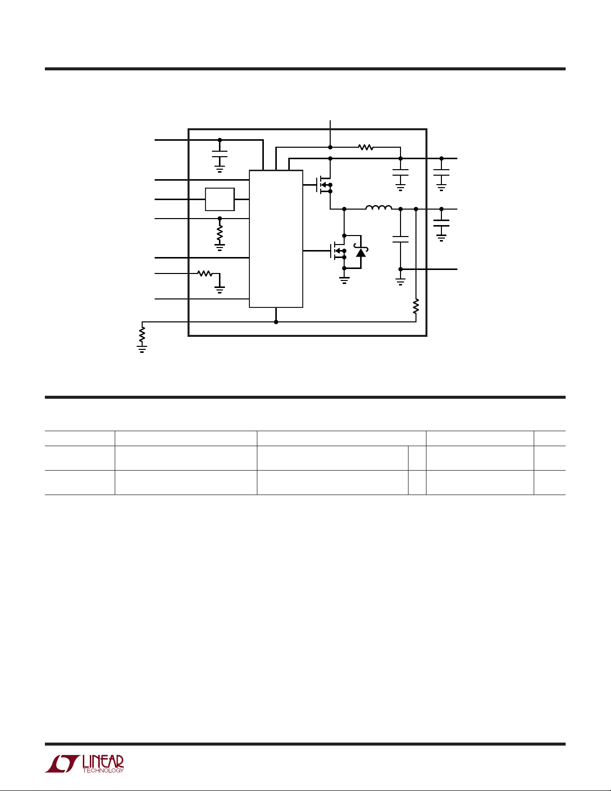
SI PLIFIEDWBLOCK DIAGRA
W
LTM4600
SV
IN
R6
66.5k
RUN/SS
PGOOD
COMP
FCB
F
ADJ
SGND
EXTV
V
OSET
1000pF
Q1
INT
COMP
4.75k
10Ω
CC
CONTROLLER
Q2
1.5µF
15µF
6.3V
LTM4600
100k
0.5%
4600 F01
V
4.5V TO 20V
IN
V
1.5V/10A MAX
OUT
PGND
C
IN
C
OUT
Figure 1. Simplifi ed LTM4600 Block Diagram
U
DECOUPLI G REQUIRE E TS
T
SYMBOL PARAMETER CONDITIONS MIN TYP MAX UNITS
C
IN
C
OUT
External Input Capacitor Requirement
(V
= 4.5V to 15V, V
IN
OUT
= 1.5V)
External Output Capacitor Requirement
(V
= 4.5V to 15V, V
IN
OUT
= 1.5V)
WU
= 25°C, VIN = 12V. Use Figure 1 confi guration.
A
= 10A 20 µF
I
OUT
= 10A, Refer to Table 2 in the
I
OUT
Applications Information Section
100 200 µF
PRERELEASE
4600p
7

LTM4600
OPERATIO
U
µModule Description
The LTM4600 is a standalone non-isolated synchronous
switching DC/DC power supply. It can deliver up to 10A of
DC output current with only bulk external input and output
capacitors. This module provides a precisely regulated
output voltage programmable via one external resistor from
0.6V
The input voltage range is 4.5V to 20V. A simplifi ed block
diagram is shown in Figure 1 and the typical application
schematic is shown in Figure 17.
The LTM4600 contains an integrated LTC constant on-time
current-mode regulator, ultra-low R
switching speed and integrated Schottky diode. The typical
switching frequency is 800kHz at full load. With current
mode control and internal feedback loop compensation,
the LTM4600 module has suffi cient stability margins and
good transient performance under a wide range of operating conditions and with a wide range of output capacitors,
even all ceramic output capacitors.
Current mode control provides cycle-by-cycle fast current
limit. In addition, foldback current limiting is provided in an
over-current condition while V
has defeatable short circuit latch off. Internal overvoltage and undervoltage comparators pull the open-drain
PGOOD output low if the output feedback voltage exits a
to 5.0VDC, not to exceed 80% of the input voltage.
DC
FETs with fast
DS(ON)
drops. Also, the LTM4600
FB
±10% window around the regulation point. Furthermore,
in an overvoltage condition, internal top FET Q1 is turned
off and bottom FET Q2 is turned on and held on until the
overvoltage condition clears.
Pulling the RUN/SS pin low forces the controller into its
shutdown state, turning off both Q1 and Q2. Releasing the
pin allows an internal 1.2µA current source to charge up
the softstart capacitor. When this voltage reaches 1.5V,
the controller turns on and begins switching.
At low load current the module works in continuous current mode by default to achieve minimum output voltage
ripple. It can be programmed to operate in discontinuous
current mode for improved light load effi ciency when the
FCB pin is pulled up above 0.8V and no higher than 5V.
The FCB pin has a 4.25k resistor to ground, so a resistor
can set the voltage on the FCB pin.
to V
IN
When EXTV
regulator powers the controller and MOSFET gate drivers.
If a minimum 4.7V external bias supply is applied on the
EXTV
internal switch connects EXTV
This eliminates the linear regulator power loss with high
input voltage, reducing the thermal stress on the controller.
The maximum voltage on EXTV
voltage should never be higher than the V
EXTV
pin, the internal regulator is turned off, and an
CC
must be sequenced after VIN.
CC
pin is grounded, an integrated 5V linear
CC
to the gate driver voltage.
CC
pin is 6V. The EXTVCC
CC
voltage. Also
IN
8
4600p
PRERELEASE

LTM4600
U
WUU
APPLICATIO S I FOR ATIO
The typical LTM4600 application circuit is shown in Figure
20. External component selection is primarily determined
by the maximum load current and output voltage.
Output Voltage Programming and Margining
The PWM controller of the LTM4600 has an internal
0.6V±1% reference voltage. As shown in the block diagram,
a 100k/0.5% internal feedback resistor connects V
FB pins. Adding a resistor R
SET
from V
pin to SGND
OSET
pin programs the output voltage:
kR
VV
=+06
O
100
.•
Table 1 shows the standard vaules of 1% R
R
SET
SET
SET
for typical output voltages:
Table 1.
R
SET
Open 100 66.5 49.9 43.2 31.6 22.1 13.7
(kΩ)
V
O
0.6 1.2 1.5 1.8 2 2.5 3.3 5
(V)
Voltage margining is the dynamic adjustment of the output
voltage to its worst case operating range in production
testing to stress the load circuitry, verify control/protection functionality of the board and improve the system
reliability. Figure 2 shows how to implement margining
function with the LTM4600. In addition to the feedback
resistor R
Turn off both transistor Q
margining. When Q
, several external components are added.
SET
UP
is on and Q
UP
and Q
DOWN
to disable the
DOWN
is off, the output
voltage is margined up. The output voltage is margined
V
LTM4600
100k
PGND SGND
OUT
V
OSET
Figure 2.
R
DOWN
Q
2N7002
R
SET
R
UP
2N7002
Q
4600 F02
OUT
resistor
DOWN
UP
and
down when Q
voltage V
needs to be margined up/down by ±M%, the
O
resistor values of R
is on and Q
DOWN
UP
and R
is off. If the output
UP
can be calculated from
DOWN
the following equations:
()••(%)
RR V M
SET UP O
()
RR k
SET UP
RV M
••(–%)
SET O
RkR
()
100
+Ω
SET DOWN
1
+
100
+Ω
1
=
=
.
06
.
06
V
V
Input Capacitors
The LTM4600 µModule should be connected to a low
ac-impedance AC source. High frequency, low ESR input
capacitors are required to be placed adjacent to the module. In Figure 20, the bulk input capacitor C
is selected
IN
for its ability to handle the large RMS current into the
converter. For a buck converter, the switching duty-cycle
can be estimated as:
V
O
D
=
V
IN
Without considering the inductor current ripple, the RMS
current of the input capacitor can be estimated as:
I
OMAX
()
%
η
DD
••()=−
1
I
CIN RMS
()
In the above equation, η% is the estimated effi ciency of
the power module. C1 can be a switcher-rated electrolytic
aluminum capacitor, OS-CON capacitor or high volume
ceramic capacitors. Note the capacitor ripple current
ratings are often based on only 2000 hours of life. This
makes it advisable to properly derate the input capacitor,
or choose a capacitor rated at a higher temperature than
required. Always contact the capacitor manufacturer for
derating requirements.
In Figure 16, the input capacitors are used as high frequency input decoupling capacitors. In a typical 10A
output application, 1-2 pieces of very low ESR X5R or
X7R, 10µF ceramic capacitors are recommended. This
decoupling capacitor should be placed directly adjacent
PRERELEASE
4600p
9

LTM4600
U
WUU
APPLICATIO S I FOR ATIO
the module input pins in the PCB layout to minimize the
trace inductance and high frequency AC noise.
Output Capacitors
The LTM4600 is designed for low output voltage ripple.
The bulk output capacitors C
effective series resistance (ESR) to meet the output voltage
ripple and transient requirements. C
tantalum capacitor, low ESR polymer capacitor or ceramic
capacitor. The typical capacitance is 200µF if all ceramic
output capacitors are used. The internally optimized loop
compensation provides suffi cient stability margin for all
ceramic capacitors applications. Additional output fi ltering may be required by the system designer, if further
reduction of output ripple or dynamic transient spike is
required. Refer to Table 2 for an output capacitance matrix
for each output voltage Droop, peak to peak deviation and
recovery time during a 5A/µs transient with a specifi c
output capacitance.
Fault Conditions: Current Limit and Over current
Foldback
The LTM4600 has a current mode controller, which inherently limits the cycle-by-cycle inductor current not only in
steady state operation, but also in transient.
To further limit current in the event of an over load condition, the LTM4600 provides foldback current limiting. If the
output voltage falls by more than 50%, then the maximum
output current is progressively lowered to about one sixth
of its full current limit value.
is chosen with low enough
OUT
can be low ESR
OUT
Soft-Start and Latchoff with the RUN/SS pin
The RUN/SS pin provides a means to shut down the
LTM4600 as well as a timer for soft-start and over-current latchoff. Pulling the RUN/SS pin below 0.8V puts
the LTM4600 into a low quiescent current shutdown (I
≤ 30µA). Releasing the pin allows an internal 1.2µA current source to charge up the timing capacitor CSS. Inside
LTM4600, there is an internal 1000pF capacitor from
RUN/SS pin to ground. If RUN/SS pin has an external
capacitor CSS_EXT to ground, the delay before starting
is about:
V
15
t
DELAY SS EXT
When the voltage on RUN/SS pin reaches 1.5V, the
LTM4600 internal switches are operating with a clamping
of the maximum output inductor current limited by the
RUN/SS pin total soft-start capacitance. As the RUN/SS pin
voltage rises to 3V, the soft-start clamping of the inductor
current is released.
to V
V
IN
OUT
There are restrictions in the maximum V
down ratio that can be achieved for a given input voltage.
These contraints are shown in the Typical Performance
Characteristics curves labeled “V
Ratio”. Note that additional thermal de-rating may apply.
See the Thermal Considerations and Output Current DeRating sections of this data sheet.
.
=
12
.
Stepdown Ratios
CpF
•( )
A
µ
_
+
1000
to V
IN
to V
IN
OUT
Stepdown
OUT
Q
step
10
4600p
PRERELEASE

LTM4600
U
WUU
APPLICATIO S I FOR ATIO
Table 2. Output Voltage Response Verses Component Matrix
TYPICAL MEASURED VALUES
C
VENDORS PART NUMBER C
OUT1
TDK C4532X5R0J107MZ (100UF,6.3V) SANYO POS CAP 6TPE330MIL (330µF, 6.3V)
TAIYO YUDEN JMK432BJ107MU-T ( 100µF, 6.3V) SANYO POS CAP 2R5TPE470M9 (470µF, 2.5V)
TAIYO YUDEN JMK316BJ226ML-T501 ( 22µF, 6.3V) SANYO POS CAP 4TPE470MCL (470µF, 4V)
V
OUT
(V)
1.2 2 × 10µF 25V 150µF 35V 3 × 22µF 6.3V 470µF 4V NONE 100pF 12 35 68 25 5
1.2 2 × 10µF 25V 150µF 35V 3 × 22µF 6.3V 470µF 4V NONE 100pF 5 35 68 25 5
1.5 2 × 10µF 25V 150µF 35V 3 × 22µF 6.3V 470µF 4V NONE 100pF 12 36 75 25 5
1.5 2 × 10µF 25V 150µF 35V 3 × 22µF 6.3V 470µF 4V NONE 100pF 5 36 75 25 5
1.8 2 × 10µF 25V 150µF 35V 3 × 22µF 6.3V 470µF 4V NONE 100pF 12 40 81 30 5
1.8 2 × 10µF 25V 150µF 35V 3 × 22µF 6.3V 470µF 4V NONE 100pF 5 40 81 30 5
2.5 2 × 10µF 25V 150µF 35V 3 × 22µF 6.3V 470µF 4V NONE 100pF 12 51 102 30 5
2.5 2 × 10µF 25V 150µF 35V 3 × 22µF 6.3V 470µF 4V NONE 100pF 5 57 116 30 5
3.3 2 × 10µF 25V 150µF 35V 3 × 22µF 6.3V 470µF 4V NONE 100pF 12 64 129 35 5
3.3 2 × 10µF 25V 150µF 35V 3 × 22µF 6.3V 470µF 4V NONE 100pF 7 82 166 35 5
1.2 2 × 10µF 25V 150µF 35V 1 × 100µF 6.3V 470µF 2.5V NONE 100pF 12 35 70 20 5
1.2 2 × 10µF 25V 150µF 35V 1 × 100µF 6.3V 470µF 2.5V NONE 100pF 5 35 70 20 5
1.5 2 × 10µF 25V 150µF 35V 1 × 100µF 6.3V 470µF 2.5V NONE 100pF 12 37 79 20 5
1.5 2 × 10µF 25V 150µF 35V 1 × 100µF 6.3V 470µF 2.5V NONE 100pF 5 37 79 20 5
1.8 2 × 10µF 25V 150µF 35V 1 × 100µF 6.3V 470µF 2.5V NONE 100pF 12 44 85 20 5
1.8 2 × 10µF 25V 150µF 35V 1 × 100µF 6.3V 470µF 2.5V NONE 100pF 5 44 88 20 5
2.5 2 × 10µF 25V 150µF 35V 1 × 100µF 6.3V 470µF 4V NONE 100pF 12 48 103 30 5
2.5 2 × 10µF 25V 150µF 35V 1 × 100µF 6.3V 470µF 4V NONE 100pF 5 48 103 30 5
3.3 2
3.3 2 × 10µF 25V 150µF 35V 1 × 100µF 6.3V 470µF 4V NONE 100pF 7 66 132 30 5
1.2 2 × 10µF 25V 150µF 35V 2 × 100µF 6.3V 330µF 6.3V NONE 100pF 12 40 80 20 5
1.2 2 × 10µF 25V 150µF 35V 2 × 100µF 6.3V 330µF 6.3V NONE 100pF 5 40 80 20 5
1.5 2 × 10µF 25V 150µF 35V 2 × 100µF 6.3V 330µF 6.3V NONE 100pF 12 44 89 20 5
1.5 2 × 10µF 25V 150µF 35V 2 × 100µF 6.3V 330µF 6.3V NONE 100pF 5 44 84 20 5
1.8 2 × 10µF 25V 150µF 35V 2 × 100µF 6.3V 330µF 6.3V NONE 100pF 12 44 91 20 5
1.8 2 × 10µF 25V 150µF 35V 2 × 100µF 6.3V 330µF 6.3V NONE 100pF 5 46 91 20 5
2.5 2 × 10µF 25V 150µF 35V 2 × 100µF 6.3V 330µF 6.3V NONE 100pF 12 56 113 30 5
2.5 2 × 10µF 25V 150µF 35V 2 × 100µF 6.3V 330µF 6.3V NONE 100pF 5 56 113 30 5
3.3 2 × 10µF 25V 150µF 35V 2 × 100µF 6.3V 330µF 6.3V NONE 100pF 12 64 126 30 5
3.3 2 × 10µF 25V 150µF 35V 2 × 100µF 6.3V 330µF 6.3V NONE 100pF 7 64 126 30 5
1.2 2 × 10µF 25V 150µF 35V 4 × 100µF 6.3V NONE NONE 100pF 12 49 98 20 5
1.2 2 × 10µF 25V 150µF 35V 4 × 100µF 6.3V NONE NONE 100pF 5 49 98 20 5
1.5 2 × 10µF 25V 150µF 35V 4 × 100µF 6.3V NONE NONE 100pF 12 54 108 20 5
1.5 2 × 10µF 25V 150µF 35V 4 × 100µF 6.3V NONE NONE 100pF 5 61 118 20 5
1.8 2 × 10µF 25V 150µF 35V 4 × 100µF 6.3V NONE NONE 100pF 12 62 125 20 5
1.8 2 × 10µF 25V 150µF 35V 4 × 100µF 6.3V NONE NONE 100pF 5 62 128 20 5
2.5 2 × 10µF 25V 150µF 35V 4 × 100µF 6.3V NONE NONE 100pF 12 70 159 25 5
2.5 2 × 10µF 25V 150µF 35V 4 × 100µF 6.3V NONE NONE 100pF 5 60 115 25 5
3.3 2 ×
3.3 2 × 10µF 25V 150µF 35V 4 × 100µF 6.3V NONE NONE 100pF 7 100 200 25 5
52 × 10µF 25V 150µF 35V 4 × 100µF 6.3V NONE NONE 100pF 15 188 375 25 5
52 × 10µF 25V 150µF 35V 4 × 100µF 6.3V NONE NONE 100pF 20 159 320 25 5
CIN
(CERAMIC)
× 10µF 25V 150µF 35V 1 × 100µF 6.3V 470µF 4V NONE 100pF 12 52 106 30 5
10µF 25V 150µF 35V 4 × 100µF 6.3V NONE NONE 100pF 12 76 144 25 5
CIN
(BULK)
C
OUT1
(CERAMIC)
C
OUT2
(BULK)
C
COMP
VENDORS PART NUMBER
OUT2
C3 VIN
(V)
DROOP
(mV)
PEAK TO PEAK
(mV)
RECOVERY TIME
(µs)
LOAD STEP
(A/µs)
PRERELEASE
4600p
11

LTM4600
U
WUU
APPLICATIO S I FOR ATIO
After the controller has been started and given adequate
time to charge up the output capacitor, CSS is used as a
short-circuit timer. After the RUN/SS pin charges above 4V,
if the output voltage falls below 75% of its regulated value,
then a short-circuit fault is assumed. A 1.8µA current then
begins discharging CSS. If the fault condition persists until
the RUN/SS pin drops to 3.5V, then the controller turns
off both power MOSFETs, shuting down the converter
permanently. The RUN/SS pin must be actively pulled
down to ground in order to restart operation.
The over-current protection timer requires the soft-start
timing capacitor CSS be made large enough to guarantee
that the output is in regulation by the time CSS has reached
the 4V threshold. In general, this will depends upon the
size of the output capacitance, output voltage and load
current characteristic. A minimum external soft-start
capacitor can be estimated from:
3
CpFCVFV
SS EXT OUT OUT S_
•([/])+>1000 10
Generally 0.1µF is more than suffi cient.
Since the load current is already limited by the current
mode control and current foldback circuitry during a
shortcircuit, over-current latchoff operation is NOT always
needed or desired, especially the output has large amount
of capacitance or the load draw huge current during start
up. The latchoff feature can be overridden by a pull-up
current greater than 5µA but less than 80µA to the RUN/SS
pin. The additional current prevents the discharge of CSS
during a fault and also shortens the soft-start period. Using a resistor from RUN/SS pin to V
–
is a simple solution
IN
to defeat latchoff. Any pull-up network must be able to
maintain RUN/SS above 4V maximum latchoff threshold
and overcome the 4µA maximum discharge current. Figure
3 shows a conceptual drawing of V
during startup and
RUN
short circuit.
V
RUN/SS
4V
3V
1.5V
SOFT-START
CLAMPING
RELEASED
OF I
L
SWITCHING
STARTS
Figure 3. RUN/SS Pin Voltage During Startup and
Short-Circuit Protection
Figure 4. Defeat Short-Circuit Latchoff with a Pull-Up
Resistor to V
SHORT-CIRCUIT
LATCH ARMED
V
IN
500k
IN
V
O
V
IN
LTM4600
RUN/SS
PGND SGND
OUTPUT
OVERLOAD
HAPPENS
4600 F04
SHORT-CIRCUIT
LATCHOFF
75%V
O
3.5V
t
t
4600 F03
12
4600p
PRERELEASE

LTM4600
U
WUU
APPLICATIO S I FOR ATIO
Enable
The RUN/SS pin can be driven from logic as shown in
Figure 5. This function allows the LTM4600 to be turned
on or off remotely. The ON signal can also control the
sequence of the output voltage.
RUN/SS
PGND
RAMP
FB1
STATUS
SDO
FB2
LTM4600
SGND
3.3V
4600 F05
V
49.9k
V
66.5k
4600 F06
V
V
LTM4600
OSET
V
V
LTM4600
OSET
IN
IN
V
1.8V
OUT
IN
IN
V
1.5V
OUT
ON
2N7002
Figure 5. Enable Circuit with External Logic
Output Voltage Tracking
For the applications that require output voltage tracking,
several LTM4600 modules can be programmed by the
power supply tracking controller such as the LTC2923.
Figure 6 shows a typical schematic with LTC2923. Coin-
V
GATE
CC
ON
LTC2923
RAMPBUF
TRACK1
TRACK2
Q1
GND
V
IN
DC/DC
5V
R
ONB
R
ONA
R
TB1
R
TA1
TB2
R
TA2
R
Figure 6. Output Voltage Tracking with the LTC2923 Controller
cident, ratiometric and offset tracking for VO rising and
falling can be implemented with different sets of resistor
values. See the LTC2923 data sheet for more details.
EXTV
Connection
CC
An internal low dropout regulator produces an internal 5V
supply that powers the control circuitry and FET drivers.
Therefore, if the system does not have a 5V power rail,
the LTM4600 can be directly powered by V
. The gate
IN
driver current through LDO is about 18mA. The internal
LDO power dissipation can be calculated as:
P
LDO_LOSS
= 18mA • (VIN – 5V)
The LTM4600 also provides an external gate driver voltage pin EXTV
recommended to connect EXTV
rail. Whenever the EXTV
. If there is a 5V rail in the system, it is
CC
pin to the external 5V
CC
pin is above 4.7V, the internal
CC
5V LDO is shut off and an internal 50mA P-channel switch
connects the EXTV
from EXTV
until this pin drops below 4.5V. Do not apply
CC
more than 6V to the EXTV
. The following list summaries the possible connec-
< V
IN
tions for EXTV
1. EXTV
grounded. Internal 5V LDO is always powered
CC
to internal 5V. Internal 5V is supplied
CC
pin and ensure that EXTVCC
CC
:
CC
from the internal 5V regulator.
2. EXTV
connected to an external supply. Internal LDO
CC
is shut off. A high effi ciency supply compatible with the
MOSFET gate drive requirements (typically 5V) can improve overall effi ciency. With this connection, it is always
required that the EXTV
pin voltage.
V
IN
voltage can not be higher than
CC
Discontinuous Operation and FCB Pin
The FCB pin determines whether the internal bottom
MOSFET remains on when the inductor current reverses.
There is an internal 4.75k pulling down resistor connecting
this pin to ground. The default light load operation mode
is forced continuous (PWM) current mode. This mode
provides minimum output voltage ripple.
PRERELEASE
4600p
13

LTM4600
U
WUU
APPLICATIO S I FOR ATIO
In the application where the light load effi ciency is important, tying the FCB pin above 0.6V threshold enables
discontinuous operation where the bottom MOSFET turns
off when inductor current reverses. Therefore, the conduction loss is minimized and light load effi cient is improved.
The penalty is that the controller may skip cycle and the
output voltage ripple increases at light load.
Paralleling Operation with Load Sharing
Two or more LTM4600 modules can be paralleled to provide
higher than 10A output current. Figure 7 shows the necessary interconnection between two paralleled modules. The
OPTI-LOOP™ current mode control ensures good current
sharing among modules to balance the thermal stress.
The new feedback equation for two or more LTM4600s
in parallel is:
k
100
VV
=+06
OUT
.•
where N is the number of LTM4600s in parallel.
V
IN
Figure 7. Parallel Two µModules with Load Sharing
OPTI-LOOP is a trademark of Linear Technology Corporation.
V
IN
PGND SGNDCOMP
V
IN
PGND
N
R
SET
R
SET
LTM4600
V
OSET
OSET
LTM4600
V
OUT
R
SET
SGNDCOMP V
V
OUT
4600 F07
V
OUT
(20A
MAX
)
Thermal Considerations and Output Current Derating
The power loss curves in Figures 8 and 13 can be used
in coordination with the load current de-rating curves in
Figures 9 to 12 and Figures 14 to 15 for calculating an
approximate θ
for the module. Each of the load current
JA
de-rating curves will lower the maximum load current
as a function of the increased ambient temperature to
keep the maximum junction temperature of the power
module at 100°C maximum. This 100°C maximum is to
allow for an increased rise of about 15°C to 20°C inside
the module. This will maintain the maximum operating
temperature to below 125°C. Each of the de-rating curves
and the power loss curve that corresponds to the correct
output voltage can be used to solve for the approximate
of the condition. Each Figure has three curves that are
θ
JA
taken at three different air fl ow conditions. For example
in Figure 9, the 10A load current can be achieved up to
60°C ambient temperature with no air fl ow. If this 60°C
is subtracted from the maximum module temperature
of 100°C, then 40°C is the maximum temperature rise.
Now Figure 8 records the power loss for this 5V to 1.5V
at the 10A output. If we take the 40°C rise and divided it
by the 3 watts of loss, then we get an approximate θ
JA
of 13.5°C/W with no heatsink. If we take the next air fl ow
curve in Figure 9 at 200LFM of air fl ow, then the maximum
ambient temperature allowed at 10A load current is 65°C.
This calculates to a 35°C rise, and an approximate θ
JA
of
11.6°C/W with no heatsink. In the next air fl ow curve at
400LFM in Figure 9, the maximum ambient temperature
allowed at 10A load current is 73°C. This calculates to
a 27°C rise, and an approximate θ
of 9°C/W with no
JA
heatsink. Each of the de-rating curves in Figures 9 to
12 or Figures 14 to 15 can be used with the appropriate
power loss curve in either fi gure 8 or fi gure 13 to derive
an approximate θ
for Figures 9 to 12, and Figures 14 to 15. A complete
θ
JA
. Table 3 and 4 provide the approximate
JA
explanation of the thermal characteristics is provided in
the thermal application note for the LTM4600.
14
4600p
PRERELEASE

LTM4600
U
WUU
APPLICATIO S I FOR ATIO
4.5
4.0
3.5
3.0
2.5
2.0
1.5
POWER LOSS (W)
1.0
0.5
0
086
Figure 8. Power Loss vs Load Current
10
9
VIN = 5V
= 1.5V
V
O
12V LOSS
24 10
OUTPUT CURRENT (A)
5V LOSS
4600 F08
10
9
VIN = 5V
= 1.5V
V
O
8
7
6
MAXIMUM LOAD CURRENT (A)
5
0 LFM
200 LFM
400 LFM
4
50 70
60 80 90
AMBIENT TEMPERATURE (°C)
Figure 9. No Heatsink
10
9
8
7
6
MAXIMUM LOAD CURRENT (A)
5
0 LFM
200 LFM
400 LFM
4
50 55 70
60 65 75 80 85 90
AMBIENT TEMPERATURE (°C)
4600 F09
VIN = 12V
= 1.5V
V
O
4600 F11
8
7
6
MAXIMUM LOAD CURRENT (A)
5
0 LFM
200 LFM
400 LFM
4
50
70
60 80 90 100
AMBIENT TEMPERATURE (°C)
Figure 10. BGA Heatsink
10
VIN = 12V
= 1.5V
V
O
9
8
7
6
5
MAXIMUM LOAD CURRENT (A)
0 LFM
4
200 LFM
400 LFM
3
50
70
60
AMBIENT TEMPERATURE (°C)
4600 F10
80 90 100
4600 F12
Figure 11. No Heatsink
PRERELEASE
Figure 12. BGA Heatsink
4600p
15

LTM4600
U
WUU
APPLICATIO S I FOR ATIO
5.0
4.5
4.0
3.5
3.0
2.5
2.0
POWER LOSS (W)
1.5
1.0
0.5
0
086
Figure 13. Power Loss vs Load Current
10
9
8
7
6
5
4
3
2
MAXIMUM LOAD CURRENT (A)
0 LFM
200 LFM
1
400 LFM
0
40 70
6050 80 90
AMBIENT TEMPERATURE (°C)
VIN = 12V
= 3.3V
V
O
4600 F14
12V LOSS
24 10
OUTPUT CURRENT (A)
4600 F13
10
VIN = 12V
= 3.3V
V
O
9
8
7
6
MAXIMUM LOAD CURRENT (A)
5
4
40 50
0 LFM
200 LFM
400 LFM
70
60 80 90 100
AMBIENT TEMPERATURE (°C)
4600 F15
16
Figure 14. No Heatsink
Figure 15. BGA Heatsink
4600p
PRERELEASE

LTM4600
U
WUU
APPLICATIO S I FOR ATIO
Table 3. 1.5V Output
DE-RATING CURVE VIN (V) POWER LOSS CURVE AIR FLOW (LFM) HEATSINK* θJA (°C/W)
Figures 9, 11 5, 12 Figure 8 0 None 13.5
Figures 9, 11 5, 12 Figure 8 200 None 11
Figures 9, 11 5, 12 Figure 8 400 None 9
Figures 10, 12 5, 12 Figure 8 0 BGA Heatsink 9.5
Figures 10, 12 5, 12 Figure 8 200 BGA Heatsink 6.25
Figures 10, 12 5, 12 Figure 8 400 BGA Heatsink 4.5
Table 4. 3.3V Output
DE-RATING CURVE VIN (V) POWER LOSS CURVE AIR FLOW (LFM) HEATSINK* θJA (°C/W)
Figure 14 12 Figure 8 0 None 13.5
Figure 14 12 Figure 8 200 None 11.6
Figure 14 12 Figure 8 400 None 10.4
Figure 15 12 Figure 8 0 BGA Heatsink 9.5
Figure 15 12 Figure 8 200 BGA Heatsink 6
Figure 15 12 Figure 8 400 BGA Heatsink 4.77
*Heatsink manufacturer: Wakefi eld Engineering #CiS20069
PRERELEASE
4600p
17

LTM4600
U
WUU
APPLICATIO S I FOR ATIO
Safety Considerations
The LTM4600 modules do not provide isolation from V
. There is no internal fuse. If required, a slow blow fuse
V
OUT
with a rating twice the maximum input current should be
provided to protect each unit from catastrophic failure.
Layout Checklist/Example
The high integration of the LTM4600 makes the PCB board
layout very simple and easy. However, to optimize its electrical and thermal performance, some layout considerations
are still necessary.
• Use large PCB copper areas for high current path, including V
, PGND and V
IN
. It helps to minimize the
OUT
PCB conduction loss and thermal stress
• Place high frequency ceramic input and output capacitors next to the V
, PGND and V
IN
pins to minimize
OUT
high frequency noise
• Place a dedicated power ground layer underneath the
unit
• To minimize the via conduction loss and reduce module
thermal stress, use multiple vias for interconnection
between top layer and other power layers
IN
to
• Do not put via directly on pad
• Use a separated SGND ground copper area for components connected to signal pins. Connect the SGND
to PGND underneath the unit
Figure 16 gives a good example of the recommended
layout.
V
IN
C
IN
PGND
V
OUT
LOAD
TOP LAYER
Figure 16. Recommended PCB Layout
4600 F16
18
4600p
PRERELEASE

TYPICAL APPLICATIO
V
IN
5V TO 20V
GND
+
C1
150µF
C3
100pF
V
OUT
R1
66.5k
REFER TO
TABLE 2
Figure 17. Typical Application, 5V to 20V Input, 0.6V to 5V Output, 10A Max
U
C4
OPT
C
IN
10µF
2x
EXTV
SV
IN
F
ADJ
V
OSET
COMP
FCB
PGOOD
SGND
CC
V
IN
(MULTIPLE PINS)
(MULTIPLE PINS)
LTM4600
PGND
(MULTIPLE PINS)
V
OUT
RUN/SS
C2
22µF
6.3V
×3
REFER TO
TABLE 2
4600 F20
C
OUT
470µF
REFER TO
TABLE 2
0.6V TO 5V
LTM4600
V
OUT
GND
PRERELEASE
4600p
19

LTM4600
TYPICAL APPLICATIO
U
Parallel Operation and Load Sharing
C8
10µF
25V
RUN/SOFT-START
C3
10µF
25V
C7
10µF
25V
C1
10µF
25V
4.5V TO 20V
EXTV
FCB
RUN
COMP
EXTV
FCB
RUN
COMP
CC
CC
V
IN
LTM4600
V
IN
LTM4600
V
= 0.6V • ([100k/N] + R
OUT
WHERE N = 2
F
SET
V
OUT
FB
SV
IN
PGOOD
PGNDSGND
F
SET
V
OUT
FB
SV
IN
PGOOD
PGNDSGND
4600 F17
2.5V
R4
15.8k
1%
C4
220pF
2.5V
R1
100k
C1, C3, C7, C8: TDK C3216X5R1E106MT
C2, C9: TAIYO YUDEN, JMK316BJ226ML-T501
C5, C10: SANYO POS CAP, 4TPE470MCL
C9
22µF
x3
C2
22µF
x3
SET
)/R
SET
C10
470µF
4V
C5
470µF
4V
2.5V AT 20A
Current Sharing Between Two
LTM4600 Modules
12
12V
IN
2.5V
OUT
20A
10
MAX
8
6
4
INDIVIDUAL SHARE
2
0
0
5
I
OUT2
10 15 20
TOTAL LOAD
I
OUT1
25
4600 F18
4600p
20
PRERELEASE

PACKAGE DESCRIPTIO
LTM4600
U
aaa Z
LGA Package
104-Lead (15mm × 15mm)
(Reference LTM DWG # 05-05-1800)
6.9865
4.4442
1.9042
0.0000
1.9058
4.4458
5.7142
3.1742
0.6342
0.6358
3.1758
5.7158
6.9421
Y
X
15
BSC
15
BSC
TOP VIEW
aaa Z
PAD 1
CORNER
4
0.15
0.10
0.15
TOLERANCE
2.72 – 2.92
0.27 – 0.37
SUBSTRATE
CAP
MOLD
20
21
19
1817
16
11
7
10
6
9
13 14 15
5
4
5.7650
4.4950
3
2
1
8
24
23
22
28 29 30 31
27
26
2.3600
32
12
25
38
37
36
35
33 34
1.0900
60
49
59
48
58
47
57
46
56
45
55
44
54
53
42 43
52
41
40
51
39
50
82
71
81
70
68 69
78 79 80
67
77
66
65
64
74 75 76
63
62
73
61
72
Z
DETAIL B
bbb Z
2.45 – 2.55
93
92
89 90 91
88
84 85 86 87
83
6.3500
104
3.8100
1.2700
0.3175
0.3175
99 100 101 102 103
1.2700
3.8100
95 96 97 98
6.3500
94
DETAIL B
3
1. DIMENSIONING AND TOLERANCING PER ASME Y14.5M-1994
2. ALL DIMENSIONS ARE IN MILLIMETERS
3
R
T
93
104
92
99 100 101 102 103
5.0800
2.5400
0.0000
12.70
NOTES:
PADS
SEE NOTES
BSC
TOP VIEW
2.5400
SUGGESTED SOLDER PAD LAYOUT
5.0800
84 85 86 87 88 89 90 91
95 96 97 98
94
83
DETAILS OF PAD #1 IDENTIFIER ARE OPTIONAL,
BUT MUST BE LOCATED WITHIN THE ZONE INDICATED.
THE PAD #1 IDENTIFIER IS A MARKED FEATURE OR A
NOTCHED BEVELED PAD
4
LAND DESIGNATION PER JESD MO-222, SPP-010
P
82
81
74 75 76 77 78 79 80
73
72
5. PRIMARY DATUM -Z- IS SEATING PLANE
L
M
N
71
60
49
70
59
48
42 43 44 45 46 47
63 64 65 66 67 68 69
52 53 54 55 56 57 58
41
40
51
62
39
50
61
aaa
eee
bbb
SYMBOL
6. THE TOTAL NUMBER OF PADS: 104
FGH
K
J
24
23
22
26 27 28 29 30 31
33 34 35 36 37 38
32
12
25
ABCDE
20
21
1918171676543
11109
13 14 15
2
1
8
YXeee
4600 02-18
M
23
19 21
18 20 22
15 17
14 16
13.93
11 13
10 12
79
68
35
24
1
BSC
BOTTOM VIEW
6.9888
6.5475
5.2775
4.0075
2.7375
1.4675
0.3175
0.0000
0.3175
1.2700
2.5400
5.7150
4.4450
6.9850
PRERELEASE
0.11 – 0.27
13.97
BSC
PAD 1
C(0.30)
21
4600p

LTM4600
PACKAGE DESCRIPTIO
PIN NAME PIN NAME PIN NAME PIN NAME PIN NAME PIN NAME PIN NAME PIN NAME
A1 - B1 V
A2 - B2 - C2 - D2 - E2 - F2 - G2 - H2 A3 V
IN
A4 - B4 - C4 - D4 - E4 - F4 - G4 - H4 A5 V
IN
A6 - B6 - C6 - D6 - E6 - F6 - G6 - H6 A7 V
IN
A8 - B8 - C8 - D8 - E8 - F8 - G8 - H8 A9 V
IN
A10 - B10 - C10 V
A11 V
IN
A12 - B12 - C12 V
A13 V
IN
A14 - B14 - C14 V
A15 FADJ B15 - C15 - D15 - E15 - F15 - G15 - H15 PGND
A16 - B16 - C16 - D16 - E16 - F16 - G16 - H16 A17 SV
IN
A18 - B18 - C18 - D18 - E18 - F18 - G18 - H18 A19 EXTVCCB19 - C19 - D19 - E19 - F19 - G19 - H19 A20 - B20 - C20 - D20 - E20 - F20 - G20 - H20 A21 V
OSET
A22 - B22 - C22 - D22 - E22 - F22 - G22 - H22 A23 - B23 COMP C23 - D23 SGND E23 - F23 RUN/SS G23 FCB H23 -
IN
B3 - C3 - D3 - E3 - F3 - G3 - H3 -
B5 - C5 - D5 - E5 - F5 - G5 - H5 -
B7 - C7 - D7 - E7 - F7 - G7 - H7 PGND
B9 - C9 - D9 - E9 - F9 - G9 - H9 PGND
B11 - C11 - D11 - E11 - F11 - G11 - H11 PGND
B13 - C13 - D13 - E13 - F13 - G13 - H13 PGND
B17 - C17 - D17 - E17 - F17 - G17 - H17 PGND
B21 - C21 - D21 - E21 - F21 - G21 - H21 -
U
Pin Assignment Tables
(Arranged by Pin Number)
C1 - D1 V
D10 - E10 V
IN
D12 - E12 V
IN
D14 - E14 V
IN
E1 - F1 V
IN
G1 PGND H1 -
IN
F10 - G10 - H10 -
IN
F12 - G12 - H12 -
IN
F14 - G14 - H14 -
IN
PIN NAME PIN NAME PIN NAME PIN NAME PIN NAME PIN NAME PIN NAME PIN NAME
J1 PGND K1 - L1 - M1 - N1 - P1 - R1 - T1 J2 - K2 - L2 PGND M2 PGND N2 PGND P2 V
OUT
R2 V
OUT
T2 V
J3 - K3 - L3 - M3 - N3 - P3 - R3 - T3 J4 - K4 - L4 PGND M4 PGND N4 PGND P4 V
OUT
R4 V
OUT
T4 V
J5 - K5 - L5 - M5 - N5 - P5 - R5 - T5 J6 - K6 - L6 PGND M6 PGND N6 PGND P6 V
OUT
R6 V
OUT
T6 V
J7 - K7 PGND L7 - M7 - N7 - P7 - R7 - T7 J8 - K8 L8 PGND M8 PGND N8 PGND P8 V
OUT
R8 V
OUT
T8 V
J9 - K9 PGND L9 - M9 - N9 - P9 - R9 - T9 J10 - K10 L10 PGND M10 PGND N10 PGND P10 V
OUT
R10 V
OUT
T10 V
J11 - K11 PGND L11 - M11 - N11 - P11 - R11 - T11 J12 - K12 - L12 PGND M12 PGND N12 PGND P12 V
OUT
R12 V
OUT
T12 V
J13 - K13 PGND L13 - M13 - N13 - P13 - R13 - T13 J14 - K14 - L14 PGND M14 PGND N14 PGND P14 V
OUT
R14 V
OUT
T14 V
J15 - K15 PGND L15 - M15 - N15 - P15 - R15 - T15 J16 - K16 - L16 PGND M16 PGND N16 PGND P16 V
OUT
R16 V
OUT
T16 V
J17 - K17 PGND L17 - M17 - N17 - P17 - R17 - T17 J18 - K18 - L18 PGND M18 PGND N18 PGND P18 V
OUT
R18 V
OUT
T18 V
J19 - K19 - L19 - M19 - N19 - P19 - R19 - T19 J20 - K20 - L20 PGND M20 PGND N20 PGND P20 V
OUT
R20 V
OUT
T20 V
J21 - K21 - L21 - M21 - N21 - P21 - R21 - T21 J22 - K22 - L22 PGND M22 PGND N22 PGND P22 V
OUT
R22 V
OUT
T22 V
J23 PGOOD K23 - L23 - M23 - N23 - P23 - R23 - T23 -
OUT
OUT
OUT
OUT
OUT
OUT
OUT
OUT
OUT
OUT
OUT
22
4600p
PRERELEASE

PACKAGE DESCRIPTIO
LTM4600
U
Pin Assignment Tables
(Arranged by Pin Number)
PIN NAME
G1 PGND
H7
H9
H11
H13
H15
H17
PGND
PGND
PGND
PGND
PGND
PGND
J1 PGND
K7
K9
K11
K13
K15
K17
L2
L4
L6
L8
L10
L12
L14
L16
L18
L20
L22
M2
M4
M6
M8
M10
M12
M14
M16
M18
M20
M22
N2
N4
N6
N8
N10
N12
N14
N16
N18
N20
N22
PGND
PGND
PGND
PGND
PGND
PGND
PGND
PGND
PGND
PGND
PGND
PGND
PGND
PGND
PGND
PGND
PGND
PGND
PGND
PGND
PGND
PGND
PGND
PGND
PGND
PGND
PGND
PGND
PGND
PGND
PGND
PGND
PGND
PGND
PGND
PGND
PGND
PGND
PGND
P2
P4
P6
P8
P10
P12
P14
P16
P18
P20
P22
R2
R4
R6
R8
R10
R12
R14
R16
R18
R20
R22
T2
T4
T6
T8
T10
T12
T14
T16
T18
T20
T22
PIN NAME
V
OUT
V
OUT
V
OUT
V
OUT
V
OUT
V
OUT
V
OUT
V
OUT
V
OUT
V
OUT
V
OUT
V
OUT
V
OUT
V
OUT
V
OUT
V
OUT
V
OUT
V
OUT
V
OUT
V
OUT
V
OUT
V
OUT
V
OUT
V
OUT
V
OUT
V
OUT
V
OUT
V
OUT
V
OUT
V
OUT
V
OUT
V
OUT
V
OUT
PIN NAME
A3
A5
A7
A9
A11
A13
B1 V
C10
C12
C14
D1 V
E10
E12
E14
F1 V
PIN NAME
V
IN
V
IN
V
IN
V
IN
V
IN
V
IN
IN
V
IN
V
IN
V
IN
IN
V
IN
V
IN
V
IN
IN
A15 FADJ
A17 SV
A19 EXTV
A21 V
IN
CC
OSET
B23 COMP
D23 SGND
F23 RUN/SS
G23 FCB
J23 PGOOD
Information furnished by Linear Technology Corporation is believed to be accurate and reliable.
no responsibility is assumed for its use. Linear Technology Corporation makes no representation that
the interconnection of its circuits as described herein will not infringe on existing patent rights.
PRERELEASE
However,
4600p
23

LTM4600
1.8V, 10A R
TYPICAL APPLICATIO
C2
10µF
25V
U
4.5V AT 20V
C1
10µF
25V
EXTV
FCB
RUN
COMP
CC
V
IN
LTM4600
egulator
C5
F
SET
V
OUT
FB
SV
IN
PGOOD
PGNDSGND
4600 F19
100pF
49.9k
1%
1.8V AT 10A
C3
R1
100k
R2
C1, C2: TDK C3216X5R1E106MT
C3: TAIYO YUDEN, JMK316BJ226ML-T501
C4: SANYO POS CAP, 4TPE470MCL
22µF
x3
PGOOD
C4
470µF
4V
24
This product contains technology licensed from Silicon Semiconductor Corporation.
PRE-RELEASE
Linear Technology Corporation
1630 McCarthy Blvd., Milpitas, CA 95035-7417
(408) 432-1900 ● FAX: (408) 434-0507
●
www.linear.com
PRERELEASE
®
4600p
LT 1105 • PRINTED IN USA
© LINEAR TECHNOLOGY CORPORATION 2005
 Loading...