

Linear Technology LTC693IS, LTC693IN, LTC693CS, LTC693CN, LTC692IS8 Datasheet
...
LTC692/LTC693
Microprocessor
Supervisory Circuits
EATU
F
■
UL Recognized
■
Guaranteed
■
1.5mA Maximum Supply Current
■
Fast (35ns Max.) On-Board Gating of RAM Chip
S
RE
®
®
Reset Assertion at VCC = 1V
Enable Signals
■
SO8 and SO16 Packaging
■
4.40V Precision Voltage Monitor
■
Power OK/Reset Time Delay:
200ms or Adjustable
■
Minimum External Component Count
■
1µA Maximum Standby Current
■
Voltage Monitor for Power Fail or
Low Battery Warning
■
Thermal Limiting
■
Performance Specified Over Temperature
■
Superior Upgrade for MAX690 Family
U
O
PPLICATI
A
■
Critical µP Power Monitoring
■
Intelligent Instruments
■
Battery-Powered Computers and Controllers
■
Automotive Systems
S
DUESCRIPTIO
The LTC692/LTC693 provide complete power supply monitoring and battery control functions for microprocessor
reset, battery backup, CMOS RAM write protection, power
failure warning and watchdog timing. A precise internal
voltage reference and comparator circuit monitor the
power supply line. When an out-of-tolerance condition
occurs, the reset outputs are forced to active states and the
Chip Enable output unconditionally write-protects external memory. In addition, the RESET output is guaranteed
to remain logic low even with VCC as low as 1V.
The LTC692/LTC693 power the active CMOS RAMs with a
charge pumped NMOS power switch to achieve low dropout and low supply current. When primary power is lost,
auxiliary power, connected to the battery input pin, powers
the RAMs in standby through an efficient PMOS switch.
For an early warning of impending power failure, the
LTC692/LTC963 provide an internal comparator with a
user-defined threshold. An internal watchdog timer is
also available, which forces the reset pins to active states
when the watchdog input is not toggled prior to a preset
time-out period.
O
A
PPLICATITYPICAL
≥ 7.5V
V
IN
+
10µF
51k
10k
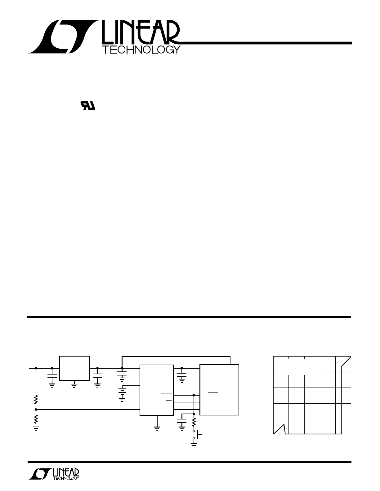
MICROPROCESSOR RESET, BATTERY BACKUP, POWER FAILURE
WARNING AND WATCHDOG TIMING ARE ALL IN A SINGLE CHIP
FOR MICROPROCESSOR SYSTEMS.
LT1086-5
V
IN
ADJ
5V
V
OUT
+
100µF
U
0.1µF
3V
RESET Output Voltage vs
Supply Voltage
5
TA = 25°C
EXTERNAL PULL-UP = 10µA
= 0V
V
4
BATT
3
2
RESET OUTPUT VOLTAGE (V)
1
0
1
0
2
SUPPLY VOLTAGE (V)
3
4
5
LTC692/3 • TA02
µP
SYSTEM
µP
POWER
LTC692/3 • TA01
0.1µF
POWER TO
CMOS RAM
µP RESET
µP NMI
I/O LINE
100Ω
V
CC
V
BATT
PFI
LTC692
LTC693
GND
V
OUT
RESET
PFO
WDI
0.1µF
1
LTC692/LTC693
A
W
O
LUTEXI T
S
A
WUW
ARB
I
Terminal Voltage
VCC.................................................... –0.3V to 6.0V
V
................................................. –0.3V to 6.0V
BATT
All Other Inputs .................. –0.3V to (V
OUT
Input Current
VCC.............................................................. 200mA
V
............................................................. 50mA
BATT
GND............................................................... 20mA
WU
/
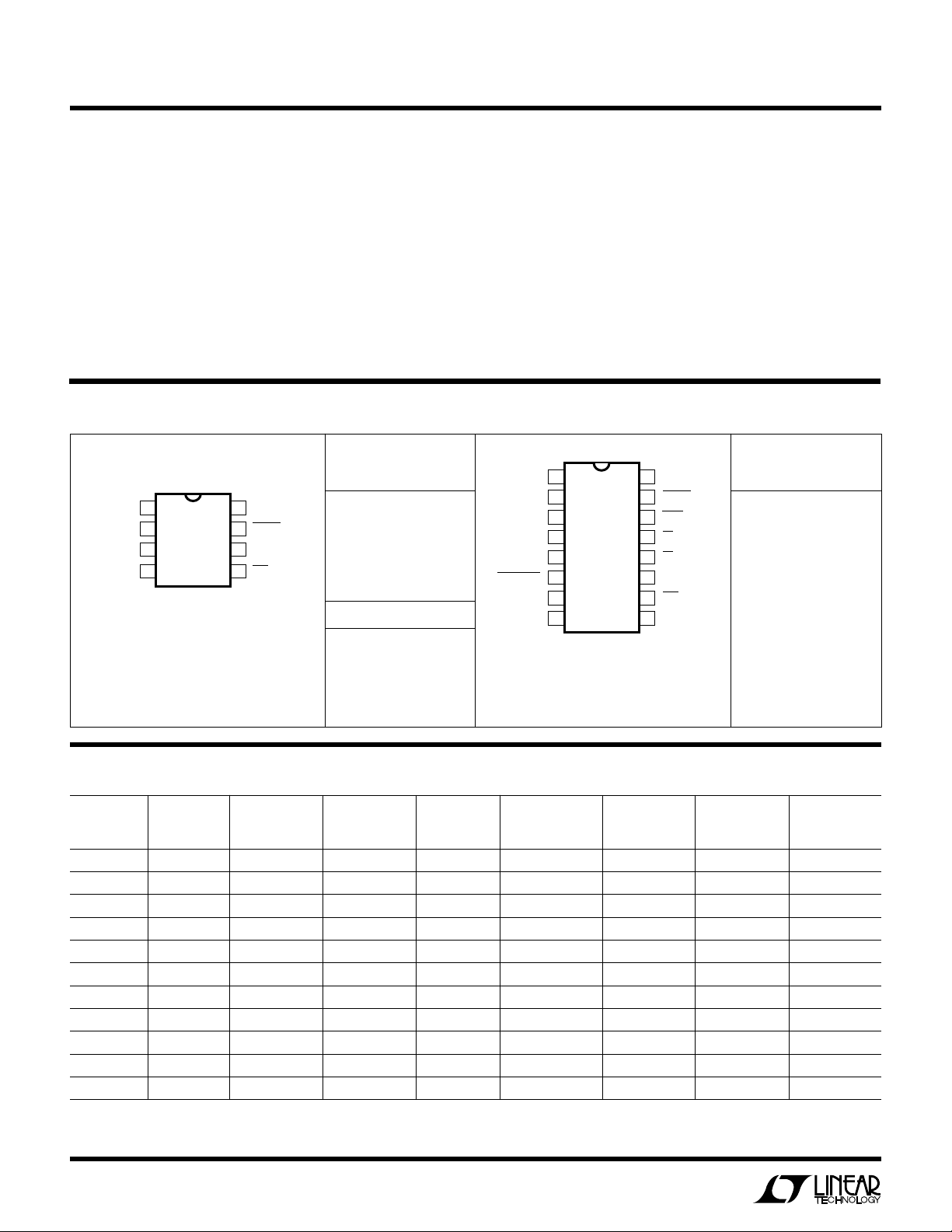
PACKAGE
V
OUT
V
CC
GND
PFI
N8 PACKAGE
8-LEAD PLASTIC DIP
T
JMAX
T
JMAX
S8 Package Conditions: PCB Mount on FR4 Material,
Still Air at 25°C, Copper Trace
O
RDER I FOR ATIO
TOP VIEW
1
2
3
4
= 110°C, θJA = 130°C/W (N)
= 110°C, θJA = 180°C/W (S)
8
7
6
5
S8 PACKAGE
8-LEAD PLASTIC SOIC
V
BATT
RESET
WDI
PFO
ORDER PART
NUMBER
LTC692CN8
LTC692IN8
LTC692CS8
LTC692IS8
S8 PART MARKING
692
692I
U
(Notes 1 and 2)
G
S
+ 0.3V)
V
Output Current .................. Short Circuit Protected
OUT
Power Dissipation............................................. 500mW
Operating Temperature Range
LTC692C/LTC693C ............................... 0°C to 70°C
LTC692I/LTC693I ............................ –40°C to 85°C
Storage Temperature Range ................ –65°C to 150°C
Lead Temperature (Soldering, 10 sec)................. 300°C
U
(Note 3)
TOP VIEW
1
V
BATT
2
V
OUT
3
V
CC
4
GND
BATT ON
LOW LINE
OSC SEL
16-LEAD PLASTIC DIP
S16 Package Conditions: PCB Mount on FR4 Material,
5
6
7
OSC IN
8
N PACKAGE
T
= 110°C, θJA = 130°C/W (N, S)
JMAX
Still Air at 25°C, Copper Trace
16-LEAD PLASTIC SOL
RESET
16
RESET
15
WDO
14
CE IN
13
CE OUT
12
WDI
11
PFO
10
PFI
9
S PACKAGE
ORDER PART
NUMBER
LTC693CN
LTC693IN
LTC693CS
LTC693IS
U
PRODUCT SELECTIO GUIDE
RESET CONDITIONAL
PINS (V) TIMER BACKUP WARNING PROTECT RESET BACKUP
LTC692 8 4.40 X X X
LTC693 16 4.40 X X X X
LTC690 8 4.65 X X X
LTC691 16 4.65 X X X X
LTC694 8 4.65 X X X
LTC695 16 4.65 X X X X
LTC699 8 4.65 X
LTC1232 8 4.37/4.62 X X
LTC1235 16 4.65 X X X X X X
LTC694-3.3 8 2.90 X X X
LTC695-3.3 16 2.90 X X X X
THRESHOLD WATCHDOG BATTERY POWER FAIL RAM WRITE PUSHBUTTON BATTERY
2
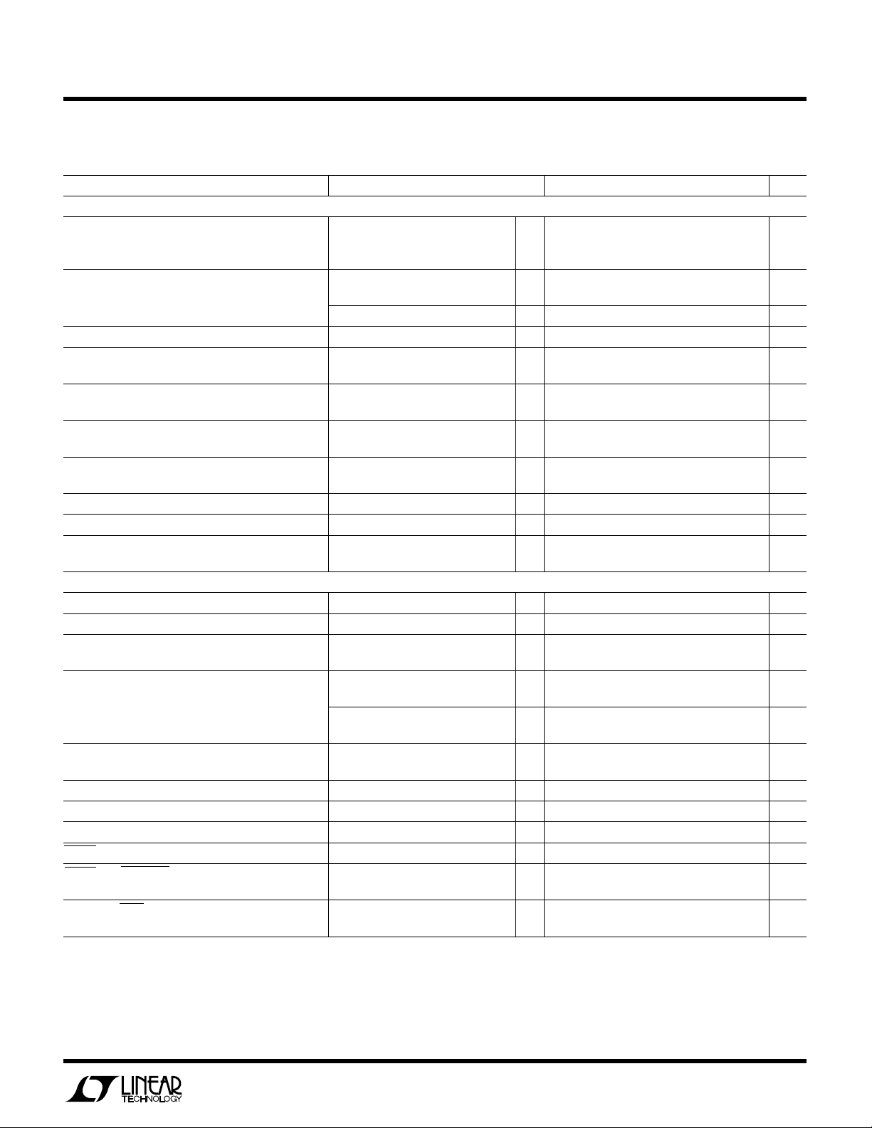
LTC692/LTC693
LECTRICAL C CHARA TERIST
E
VCC = Full Operating Range, V
PARAMETER CONDITONS MIN TYP MAX UNITS
Battery Backup Switching
Operating Voltage Range
V
CC
V
BATT
V
Output Voltage I
OUT
V
in Battery Backup Mode I
OUT
Supply Current (Exclude I
Supply Current in Battery Backup Mode VCC = 0V, V
Battery Standby Current 5.5 > VCC > V
(+ = Discharge, – = Charge) ● –1.0 0.10 µA
Battery Switchover Threshold Power Up 70 mV
VCC – V
BATT
Battery Switchover Hysteresis 20 mV
BATT ON Output Voltage (Note 4) I
BATT ON Output Short-Circuit Current (Note 4) BATT ON = V
Reset and Watchdog Timer
Reset Voltage Threshold ● 4.25 4.40 4.50 V
Reset Threshold Hysteresis 40 mV
Reset Active Time OSC SEL HIGH, VCC = 5V 160 200 240 ms
(Note 5)
Watchdog Time-Out Period, Long Period, VCC = 5V 1.2 1.6 2.00 sec
Internal Oscillator
Watchdog Time-Out Period, External Clock Long Period 4032 4097 Clock
(Note 6) Short Period 960 1025 Cycles
Reset Active Time PSRR 1 ms/V
Watchdog Time-Out Period PSRR, Internal OSC 1 ms/V
Minimum WDI Input Pulse Width VIL = 0.4V, VIH = 3.5V ● 200 ns
RESET Output Voltage At VCC = 1V I
RESET and LOW LINE Output Voltage I
(Note 4) I
RESET and WDO Output Voltage I
(Note 4) I
)I
OUT
= 2.8V, TA = 25°C, unless otherwise noted.
BATT
ICS
4.50 5.50 V
2.00 4.00 V
= 1mA V
OUT
I
= 50mA VCC – 0.50 VCC – 0.250 V
OUT
= 250µA, VCC < V
OUT
≤ 50mA 0.6 1.5 mA
OUT
BATT
Power Down 50 mV
= 3.2mA 0.4 V
SINK
BATT ON = 0V Source Current 0.5 1 25 µA
Short Period, VCC = 5V 80 100 120 ms
SINK
SINK
SOURCE
SINK
SOURCE
OUT
= 10µA, VCC = 1V 4 200 mV
= 1.6mA, VCC = 4.25V 0.4 V
= 1µA, VCC = 5V 3.5 V
= 1.6mA, VCC = 5V 0.4 V
= 1µA, VCC = 4.25V 3.5 V
BATT
= 2.8V 0.04 1 µA
+ 0.2V –0.1 0.02 µA
BATT
Sink Current 35 mA
● V
● 0.6 2.5 mA
● 0.04 5 µA
● 140 200 280 ms
● 1.0 1.6 2.25 sec
● 70 100 140 ms
– 0.05 V
CC
– 0.10 VCC – 0.005 V
CC
V
– 0.1 V
BATT
– 0.005 V
CC
– 0.02 V
BATT
3
LTC692/LTC693
LECTRICAL C CHARA TERIST
E
VCC = Full Operating Range, V
PARAMETER CONDITONS MIN TYP MAX UNITS
RESET, RESET, WDO, LOW LINE Output Source Current 1 3 25 µA
Output Short-Circuit Current (Note 4) Output Sink Current 25 mA
WDI Input Threshold Logic Low 0.8 V
WDI Input Current WDI = V
Power Fail Detector
PFI Input Threshold VCC = 5V ● 1.25 1.3 1.35 V
PFI Input Threshold PSRR 0.3 mV/V
PFI Input Current ±0.01 ±25 nA
PFO Output Voltage (Note 4) I
PFO Short Circuit Source Current PFI = HIGH, PFO = 0V 1 3 25 µA
(Note 4) PFI = LOW, PFO = V
PFI Comparator Response Time (falling) ∆VIN = –20mV, VOD = 15mV 2 µs
PFI Comparator Response Time (rising) ∆VIN = 20mV, VOD = 15mV 40 µs
(Note 4) with 10kΩ Pull-Up 8 µs
Chip Enable Gating
CE IN Threshold V
CE IN Pullup Current (Note 7) 3 µA
CE OUT Output Voltage I
CE Propagation Delay VCC = 5V, CL = 20pF 20 35 ns
CE OUT Output Short Circuit Current Output Source Current 30 mA
Oscillator
OSC IN Input Current (Note 7) ±2 µA
OSC SEL Input Pull-Up Current (Note 7) 5 µA
OSC IN Frequency Range OSC SEL = 0V ● 0 250 kHz
OSC IN Frequency with External Capacitor OSC SEL = 0V, C
= 2.8V, TA = 25°C, unless otherwise noted.
BATT
ICS
Logic High 3.5 V
OUT
WDI = 0V
= 3.2mA 0.4 V
SINK
= 1µA 3.5 V
I
SOURCE
OUT
IL
V
IH
= 3.2mA 0.4 V
SINK
= 3.0mA V
I
SOURCE
= 1µA, VCC = 0V V
I
SOURCE
Output Sink Current 35 mA
= 47pF 4 kHz
OSC
● 450µA
● –50 –8 µA
25 mA
0.8 V
2.0 V
– 1.50 V
OUT
– 0.05 V
OUT
● 20 45 ns
The ● denotes specifications which apply over the full operating
temperature range.
Note 1: Absolute maximum ratings are those values beyond which the life
of the device may be impaired.
Note 2: All voltage values are with respect to GND.
Note 3: For military temperature range, consult the factory.
Note 4: The output pins of BATT ON, LOW LINE, PFO, WDO, RESET and
RESET have weak internal pull-ups of typically 3µA. However, external
pull-up resistors may be used when higher speed is required.
4
Note 5: The LTC692/LTC693 have minimum reset active times of 140ms
(200ms typically). The reset active time of the LTC693 can be adjusted
(see Table 2 in Applications Information Section).
Note 6: The external clock feeding into the circuit passes through the
oscillator before clocking the watchdog timer (See BLOCK DIAGRAM).
Variation in the time-out period is caused by phase errors which occur
when the oscillator divides the external clock by 64. The resulting variation
in the time-out period is 64 clocks plus one clock of jitter.
Note 7: The input pins of CE IN, OSC IN and OSC SEL have weak internal
pull-ups which pull to the supply when the input pins are floating.
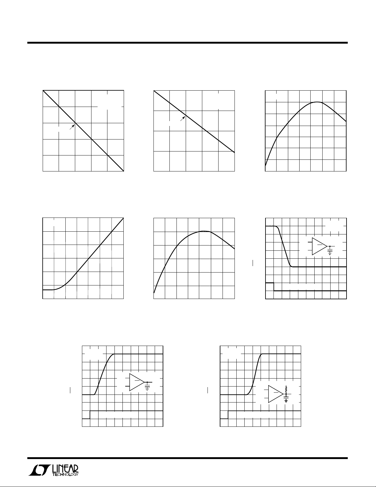
LPER
TIME (µs)
0
4
5
6
4
LTC692/3 • TPC06
3
2
0
123
5
1
1.305V
1.285V
87
6
VCC = 5V
T
A
= 25°C
+
–
V
PFI
1.3V
PFO
30pF
V
PFI
= 20mV STEP
PFO OUTPUT VOLTAGE (V)
V
vs I
OUT
5.00
4.95
4.90
4.85
OUTPUT VOLTAGE (V)
4.80
OUT
SLOPE = 5Ω
F
O
R
VCC = 5V
V
BATT
= 25°C
T
A
ATYPICA
= 2.8V
UW
CCHARA TERIST
E
C
V
vs I
OUT
2.80
2.78
SLOPE = 125Ω
2.76
OUTPUT VOLTAGE (V)
2.74
OUT
ICS
VCC = 0V
V
BATT
= 25°C
T
A
= 2.8V
LTC692/LTC693
Power Failure Input Threshold
vs Temperature
1.308
VCC = 5V
1.306
1.304
1.302
1.300
1.298
PFI INPUT THRESHOLD (V)
1.296
4.75
232
224
216
208
200
RESET ACTIVE TIME
192
184
–50
10
0
20
LOAD CURRENT (mA)
Reset Active Time vs
Temperature
VCC = 5V
50 100 125
–25 0
25 75
TEMPERATURE (°C)
Power Fail Comparator
Response Time
6
VCC = 5V
5
T
A
4
3
2
1
PFO OUTPUT VOLTAGE (V)
0
1.315V
1.295V
0
30
= 25°C
40
LTC692/3 • TPC01
LTC692/3 • TPC04
V
PFI
40
20
50
V
PFI
1.3V
= 20mV STEP
60
10080
TIME (µs)
2.72
100
0
Reset Voltage Threshold
vs Temperature
4.41
4.40
4.39
4.38
4.37
RESET VOLTAGE THRESHOLD (V)
4.36
4.35
–50
–25 0
+
PFO
140
120
LTC692/3 • TPC07
30pF
180160
–
300
200
LOAD CURRENT (µA)
50 100 125
25 75
TEMPERATURE (°C)
1.315V
1.295V
1.294
400
LTC692/3 • TPC02
500
–50
–25 0
Power Fail Comparator
Response Time
LTC692/3 • TPC05
Power Fail Comparator Response
Time with Pull-Up Resistor
6
VCC = 5V
5
= 25°C
T
A
4
3
2
1
PFO OUTPUT VOLTAGE (V)
0
0
2
V
= 20mV STEP
PFI
4
V
PFI
1.3V
6
TIME (µs)
108
+
PFO
–
12
LTC692/3 • TPC08
25 75
TEMPERATURE (°C)
5V
10k
30pF
14
1816
50 100 125
LTC692/3 • TPC03
5
 Loading...