

FEATURES
■
2 Channels with Independent Gain Control
LTC6912-1: (0, 1, 2, 5, 10, 20, 50, and 100V/V)
LTC6912-2: (0, 1, 2, 4, 8, 16, 32, and 64V/V)
■
Offset Voltage = 2mV Max (–40°C to 85°C)
■
Channel-to-Channel Gain Matching of 0.1dB Max
■
3-Wire SPITM Interface
■
Extended Gain-Bandwidth at High Gains
■
Wired-OR Outputs Possible (2:1 Analog MUX
Function)
■
Low Power Hardware Shutdown (GN-16 Only,
2µA Max at 2.7V)
■
Rail-to-Rail Input Range
■
Rail-to-Rail Output Swing
■
Single or Dual Supply: 2.7V to 10.5V Total
■
Input Noise: 12.6nV/√Hz
■
Total System Dynamic Range to 115dB
■
16-Pin GN (SSOP) or 12-Pin DFN Package Options
U
APPLICATIO S
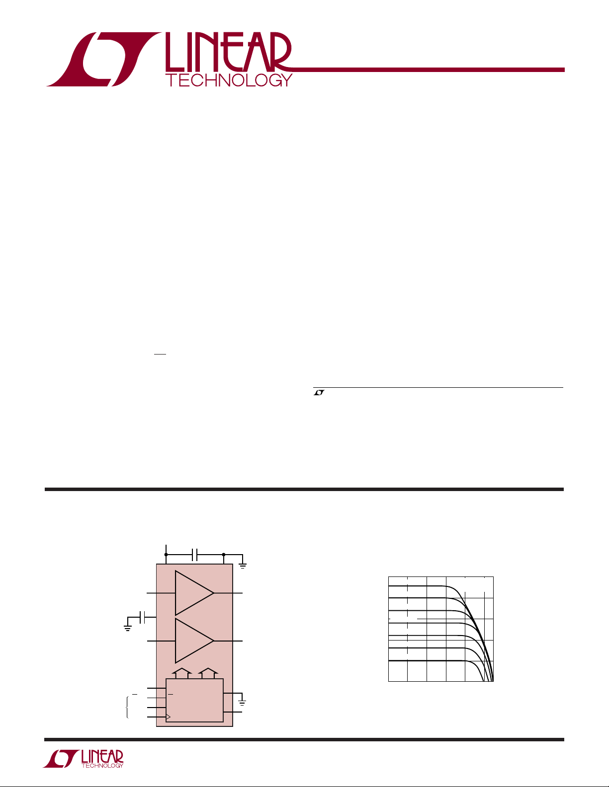
LTC6912
Dual Programmable
Gain Amplifiers with
Serial Digital Interface
U
DESCRIPTIO
The LTC®6912 is a family of dual channel, low noise,
digitally programmable gain amplifiers (PGA) that are
easy to use and occupy very little PC board space. The
gains for both channels are independently programmable
using a 3-wire SPI interface to select voltage gains of 0, 1,
2, 5, 10, 20, 50, and 100V/V (LTC6912-1 ); and 0, 1, 2, 4,
8, 16, 32, and 64V/V (LTC6912-2). All gains are inverting.
The LTC6912 family consists of 2 matched amplifiers with
rail-to-rail outputs. When operated with unity gain, they
will also process rail-to-rail input signals. A half-supply
reference generated internally at the AGND pin supports
single power supply applications. Operating from single
or split supplies from 2.7V to 10.5V total, the LTC6912-X
family is offered in tiny SSOP and DFN-12 Packages.
, LTC and LT are registered trademarks of Linear Technology Corporation.
All other trademarks are the property of their respective owners.
■
Data Acquisition Systems
■
Dynamic Gain Changing
■
Automatic Ranging Circuits
■
Automatic Gain Control
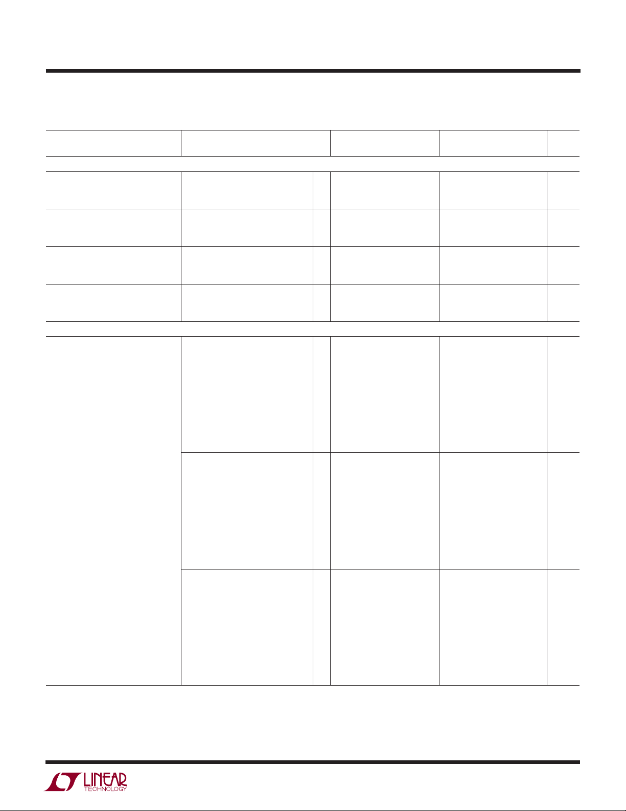
TYPICAL APPLICATIO
A Dual, Matched Low Noise PGA (16-Lead SSOP Package)
3V
12 14
+
V
2
INA
V
INA
1µF
3
AGND
4
INB
V
INB
CHB CHA
5
3-WIRE
INTERFACE
SHDN
CS/LD
DATA
SPI
CLK
SHDN
6
CS/LD
7
D
IN
8
0.1µF
LTC6912-X
U
DGND
D
OUT
V
OUT A
OUT B
LTC6912-2
–
15
V
= GAINA • V
OUTA
13
V
OUTB
10
9
= GAINB • V
INA
INB
6912 TA01a
Frequency Response
40
GAIN OF 64
GAIN OF 32
30
GAIN OF 16
20
GAIN OF 8
GAIN OF 4
GAIN (dB)
10
GAIN OF 2
GAIN OF 1
0
–10
0.1
1
FREQUENCY (kHz)
VS = ±2.5V
V
IN
10 100 1000
= 10mV
RMS
10000
6912 TA01b
6912fa
1
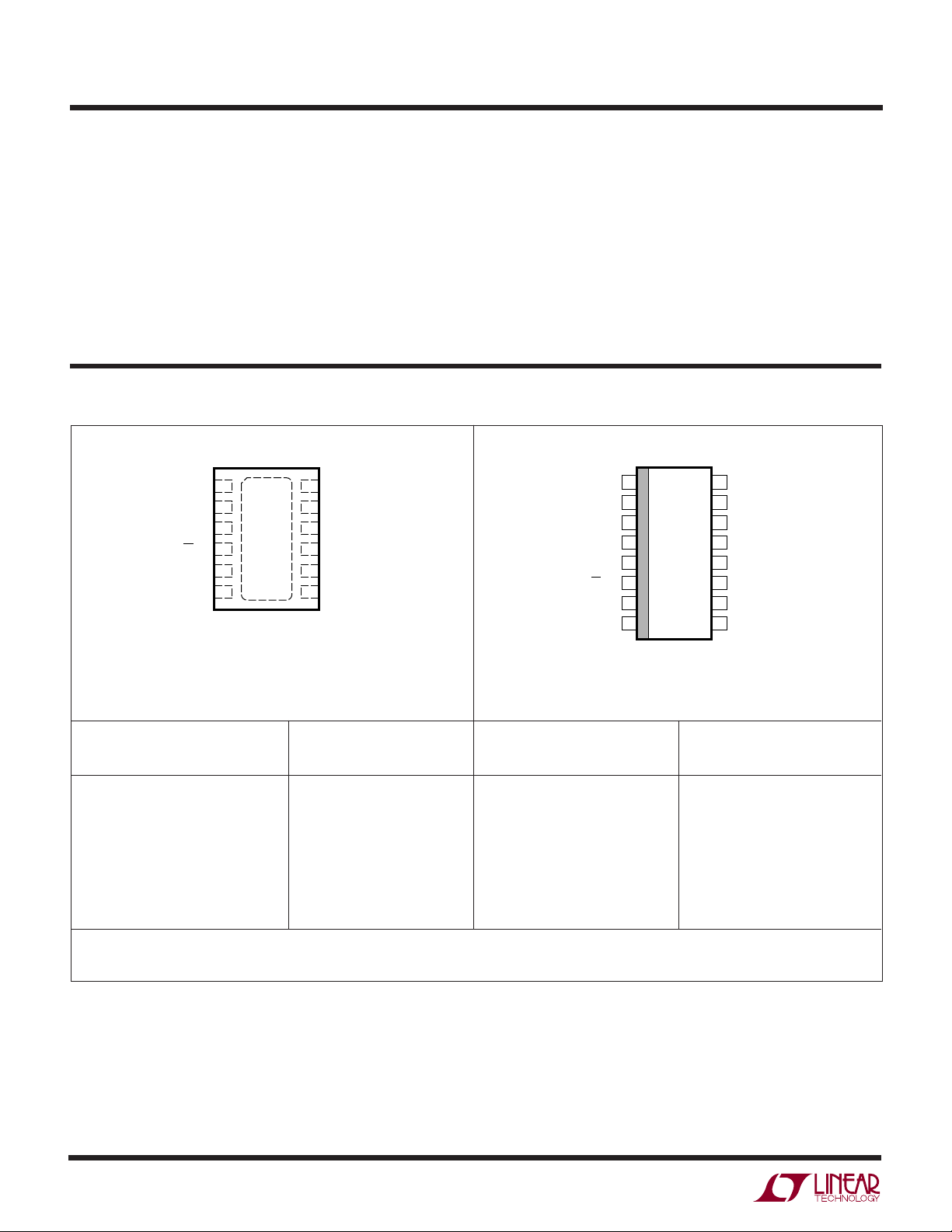
LTC6912
TOP VIEW
GN PACKAGE
16-LEAD NARROW PLASTIC SSOP
1
2
3
4
5
6
7
8
16
15
14
13
12
11
10
9
NC
INA
AGND
INB
SHDN
CS/LD
D
IN
CLK
NC
OUT A
V
–
OUT B
V
+
NC
DGND
D
OUT
WW
W
U
ABSOLUTE AXI U RATI GS
(Note 1)
Total Supply Voltage (V+ to V–) ............................... 11V
Input Current ...................................................... ±10mA
Operating Temperature Range (Note 2)
LTC6912C-1, LTC6912C-2 .................. –40°C to 85°C
LTC6912I-1, LTC6912I-2..................... –40°C to 85°C
LTC6912H-1, LTC6912H-2
(GN-16 Only) .....................................–40°C to 125°C
UUW
PACKAGE/ORDER I FOR ATIO
TOP VIEW
INA
AGND
INB
CS/LD
DIN
CLK
1
2
3
4
5
6
12
OUTA
–
11
V
OUTB
10
13
+
V
9
DGND
8
DOUT
7
Specified Temperature Range (Note 3)
LTC6912C-1, LTC6912C-2 .................. –40°C to 85°C
LTC6912I-1, LTC6912I-2..................... –40°C to 85°C
LTC6912H-1, LTC6912H-2
(GN-16 Only) .....................................–40°C to 125°C
Storage Temperature Range ..................–65°C to 150°C
UE Package ....................................... –65°C to 125°C
Lead Temperature (Soldering, 10sec)................... 300°C
Order Options Tape and Reel: Add #TR Lead Free: Add #PBF Lead Free Tape and Reel: Add #TRPBF
Lead Free Part Marking: http://www.linear.com/leadfree/
Consult LTC Marketing for parts specified with wider operating temperature ranges. *The temperature grade is identified by a label on the shipping container.
2
12-LEAD (4mm × 3mm) PLASTIC DFN
EXPOSED PAD IS CONNECTED TO V
UE12 PACKAGE
MUST BE SOLDERED TO PCB
T
= 125°C, θJA = 160°C/W
JMAX
ORDER PART
NUMBER
LTC6912CDE-1
LTC6912IDE-1
LTC6912CDE-2
LTC6912IDE-2
–
(PIN 13),
DFN PART*
MARKING
69121
69121
69122
69122
T
JMAX
ORDER PART
NUMBER
LTC6912CGN-1
LTC6912IGN-1
LTC6912HGN-1
LTC6912CGN-2
LTC6912IGN-2
LTC6912HGN-2
= 150°C, θJA = 120°C/W
GN PART
MARKING
69121
6912I1
6912H1
69122
6912I2
6912H2
6912fa
LTC6912
UUU
GAI SETTI GS A D PROPERTIES
Table 1. LTC6912-1 GAIN SETTINGS AND PROPERTIES
UPPER/LOWER NOMINAL
NIBBLE VOLTAGE GAIN MAXIMUM LINEAR INPUT RANGE (V
Q7 Q6 Q5 Q4 Dual 5V Single 5V Single 3V NOMINAL INPUT NOMINAL OUTPUT
Q3 Q2 Q1 Q0 Volts/Volt dB Supply Supply Supply IMPEDANCE (kΩ) IMPEDANCE (Ω)
0000 0 –120 10 5 3 (Open) 0.4
0001 –1 0 10 5 3 10 0.7
0010 –2 6 5 2.5 1.5 5 3.4
0011 –5 14 2 1 0.6 2 3.4
0100 –10 20 1 0.5 0.3 1 3.4
0101 –20 26 0.5 0.25 0.15 1 6.4
0110 –50 34 0.2 0.1 0.06 1 15
0111 –100 40 0.1 0.05 0.03 1 30
1 0 X X 0 –120 10 5 3 (Open) (Open)
1 1 X X Not Used (Note 11) Not Used
Table 2. LTC6912-2 GAIN SETTINGS AND PROPERTIES
UPPER/LOWER NOMINAL
NIBBLE VOLTAGE GAIN MAXIMUM LINEAR INPUT RANGE (V
Q7 Q6 Q5 Q4 Dual 5V Single 5V Single 3V NOMINAL INPUT NOMINAL OUTPUT
Q3 Q2 Q1 Q0 Volts/Volt dB Supply Supply Supply IMPEDANCE (kΩ) IMPEDANCE (Ω)
0000 0 –120 10 5 3 (Open) 0.4
0001 –1 0 10 5 3 10 0.7
0010 –2 6 5 2.5 1.5 5 3.4
0011 –4 12 2.5 1.25 0.75 2.5 3.4
0100 –8 18.1 1.25 0.625 0.375 1.25 3.4
0101 –16 24.1 0.625 0.3125 0.188 1.25 6.4
0110 –32 30.1 0.3125 0.156 0.094 1.25 15
0111 –64 36.1 0.156 0.078 0.047 1.25 30
1 0 X X 0 –120 10 5 3 (Open) (Open)
1 1 X X Not Used (Note 11) Not Used
P-P
P-P
)
)
6912fa
3
LTC6912
ELECTRICAL CHARACTERISTICS
temperature range, otherwise specifications are at T
The ● denotes the specifications that apply over the full operating
= 25°C. VS = 5V, AGND = 2.5V, Gain = 1, RL = 10k to midsupply point, unless
A
otherwise noted.
C, I GRADES H GRADE
PARAMETER CONDITIONS MIN TYP MAX MIN TYP MAX UNITS
Specifications for Both the LTC6912-1 and the LTC6912-2
Total Supply Voltage (VS)
Supply Current per Channel Both Amplifiers Active (Gain = 1)
= 2.7V, V
V
S
= 5V, V
V
S
V
= ±5V, V
S
INA
INA
INA
= V
= V
= V
INB
INB
INB
= V
= V
= 0V
AGND
AGND
Supply Current per Channel Both Amplifiers Inactive (State 1000)
(Software Shutdown) V
= 2.7V, V
S
= 5V, V
V
S
V
= ±5V, V
S
Total-Supply Current VS = 2.7V, V
(Hardware Shutdown, V
GN-16 Package Only) V
= 5V, V
S
= ±5V, V
S
INA
INA
INA
SHDN
SHDN
SHDN
= V
= V
= V
= 4.5V
= 4.5V
= V
INB
= V
INB
= 0V
INB
= 2.43V
AGND
AGND
Output Voltage Swing LOW VS = 2.7V, RL = 10k Tied to Midsupply Point
(Note 4) V
= 2.7V, RL = 500Ω Tied to Midsupply Point
S
VS = 5V, RL = 10k Tied to Midsupply Point
V
= 5V, RL = 500Ω Tied to Midsupply Point
S
VS = ±5V, RL = 10k Tied to 0V
= ±5V, RL = 500Ω Tied to 0V
V
S
Output Voltage Swing HIGH VS = 2.7V, RL = 10k Tied to Midsupply Point
(Note 4) V
= 2.7V, RL = 500Ω Tied to Midsupply Point
S
VS = 5V, RL = 10k Tied to Midsupply Point
V
= 5V, RL = 500Ω Tied to Midsupply Point
S
VS = ±5V, RL = 10k Tied to 0V
V
= ±5V, RL = 500Ω Tied to 0V
S
Output Short-Circuit Current VS = 2.7V
(Note 5) V
AGND Open-Circuit Voltage VS = Single 5V Supply, V
(GN-16 Package Only) V
= ±5V
S
= Single 5V Supply, V
S
= 0.5V
SHDN
= 4.5V 2.65 2.65 V
SHDN
AGND (Common Mode) VS = Single 2.7V Supply
Input Voltage Range V
AGND Rejection (i.e., Common VS = 2.7V, V
Mode Rejection or CMRR) V
= Single 5V Supply
S
= ±5V
V
S
= ±5V, V
S
AGND
AGND
= 1.1V to 1.6V
= –2.5V to 2.5V
Power Supply Rejection Ratio (PSRR) VS =2.7V to ±5V
Slew Rate Gain = 1
= 5V, V
V
S
V
= ±5V, V
S
OUTA
OUTA
= V
= 1.1V to 3.9V 12 12 V/µs
OUTB
= V
= ±1.4V 16 16 V/µs
OUTB
Gain = 10 (–1), Gain = 8 (–2)
= 5V, V
V
S
= ±5V, V
V
S
OUTA
OUTA
= V
= 1.1V to 3.9V 20 20 V/µs
OUTB
= V
= ±1.4V 26 26 V/µs
OUTB
Signal Attenuation at Gain = 0 Setting Gain = 0 (Digital Inputs 0000),
f = 200kHz
Signal Attenuation in Software (State = 1000)
Shutdown
●
2.7 10.5 2.7 10.5 V
●
●
●
●
●
●
●
●
●
●
●
●
●
●
●
●
●
●
●
●
●
●
●
●
●
●
●
●
●
●
●
●
1.75 2.75 1.75 3.0 mA
2.0 3.0 2.0 3.25 mA
2.25 3.5 2.25 3.75 mA
150 255 150 280 µA
200 325 200 350 µA
265 750 265 750 µA
0.3 2 0.3 5 µA
3.6 10 3.6 10 µA
20 50 20 50 µA
12 30 12 35 mV
60 110 50 125 mV
20 40 20 45 mV
100 170 90 190 mV
30 50 30 60 mV
190 260 80 290 mV
10 20 10 25 mV
50 80 50 90 mV
15 30 15 35 mV
90 160 80 175 mV
20 40 20 45 mV
180 250 180 270 mV
±27 ±27 mA
±35 ±35 mA
2.45 2.5 2.55 2.45 2.5 2.55 V
0.55 1.6 0.55 1.6 V
0.75 3.65 0.75 3.65 V
–4.3 3.2 –4.3 3.2 V
55 80 50 80 dB
55 75 50 75 dB
60 80 57 80 dB
–120 –120 dB
–120 –120 dB
4
6912fa
LTC6912
ELECTRICAL CHARACTERISTICS
temperature range, otherwise specifications are at T
The ● denotes the specifications that apply over the full operating
= 25°C. VS = 5V, AGND = 2.5V, Gain = 1, RL = 10k to midsupply point, unless
A
otherwise noted.
C, I GRADES H GRADE
PARAMETER CONDITIONS MIN TYP MAX MIN TYP MAX UNITS
Specifications for Both the LTC6912-1 and the LTC6912-2
SHDN Input High Voltage VS = Single 2.7V
(GN-16 Package Only) V
= Single 5V
S
V
= ±5V
S
SHDN Input Low Voltage VS = Single 2.7V
(GN-16 Package Only) V
= Single 5V
S
= ±5V
V
S
SHDN Pin 5, Input High Current VS = Single 2.7V 0.2 0.2 µA
(GN-16 Package Only) V
= Single 5V 1 1 µA
S
= ±5V 1 1 µA
V
S
SHDN Pin 5, Input Low Current VS = Single 2.7V 0.2 0.2 µA
(GN-16 Package Only) V
= Single 5V 1 1 µA
S
V
= ±5V 1 1 µA
S
Specifications for the LTC6912-1 ONLY
Voltage Gain (Note 6) VS = 2.7V, Gain = 1, RL = 10k
V
= 2.7V, Gain = 1, RL = 500Ω
S
= 2.7V, Gain = 2, RL = 10k
V
S
= 2.7V, Gain = 5, RL = 10k
V
S
V
= 2.7V, Gain = 10, RL =10k
S
= 2.7V, Gain = 10, RL = 500Ω
V
S
= 2.7V, Gain = 20, RL = 10k
V
S
V
= 2.7V, Gain = 50, RL = 10k
S
= 2.7V, Gain = 100, RL = 10k
V
S
= 2.7V, Gain = 100, RL = 500Ω
V
S
VS = 5V, Gain = 1, RL = 10k
V
= 5V, Gain = 1, RL = 500Ω
S
= 5V, Gain = 2, RL = 10k
V
S
= 5V, Gain = 5, RL = 10k
V
S
V
= 5V, Gain = 10, RL = 10k
S
= 5V, Gain = 10, RL = 500Ω
V
S
= 5V, Gain = 20, RL = 10k
V
S
V
= 5V, Gain = 50, RL = 10k
S
= 5V, Gain = 100, RL = 10k
V
S
= 5V, Gain = 100, RL = 500Ω
V
S
VS = ±5V, Gain = 1, RL = 10k
V
= ±5V, Gain = 1, RL = 500Ω
S
= ±5V, Gain = 2, RL = 10k
V
S
= ±5V, Gain = 5, RL = 10k
V
S
V
= ±5V, Gain = 10, RL = 10k
S
= ±5V, Gain = 10, RL = 500Ω
V
S
= ±5V, Gain = 20, RL = 10k
V
S
V
= ±5V, Gain = 50, RL = 10k
S
= ±5V, Gain = 100, RL = 10k
V
S
= ±5V, Gain = 100, RL = 500Ω
V
S
●
2.43 2.43 V
●
4.5 4.5 V
●
4.5 4.5 V
●
●
●
●
–0.07 0 0.07 –0.08 0 0.07 dB
●
–0.11 –0.02 0.07 – 0.13 – 0.02 0.07 dB
●
5.94 6.01 6.08 5.93 6.01 6.08 dB
●
13.85 13.95 14.05 13.8 13.95 14.05 dB
●
19.7 19.93 20.1 19.65 19.93 20.1 dB
●
19.55 19.85 20.05 19.35 19.85 20.05 dB
●
25.75 25.94 26.1 25.65 25.94 26.1 dB
●
33.5 33.8 34.05 33.40 33.8 34.05 dB
●
39.2 39.6 40.0 39.0 39.6 40.0 dB
●
37.3 38.9 39.7 36.20 38.9 39.7 dB
●
–0.08 0.01 0.08 –0.09 0.01 0.08 dB
●
–0.11 –0.01 0.07 – 0.13 – 0.01 0.07 dB
●
5.95 6.02 6.09 5.94 6.02 6.09 dB
●
13.8 13.96 14.1 13.78 13.96 14.1 dB
●
19.8 19.94 20.1 19.75 19.94 20.1 dB
●
19.6 19.87 20.1 19.45 19.87 20.1 dB
●
25.78 25.94 26.08 25.75 25.94 26.08 dB
●
33.5 33.84 34.1 33.4 33.84 34.1 dB
●
39.3 39.7 40.1 39.1 39.7 40.1 dB
●
37.75 39.2 39.85 36.6 39.2 39.85 dB
●
–0.06 0.01 0.08 –0.07 0.01 0.08 dB
●
–0.10 0 0.08 –0.11 0 0.08 dB
●
5.95 6.02 6.09 5.94 6.02 6.09 dB
●
13.8 13.96 14.1 13.79 13.96 14.1 dB
●
19.78 19.94 20.08 19.75 19.94 20.08 dB
●
19.68 19.91 20.05 19.58 19.91 20.05 dB
●
25.78 25.95 26.08 25.73 25.95 26.08 dB
●
33.65 33.87 34.05 33.60 33.87 34.05 dB
●
39.4 39.8 40.2 39.25 39.8 40.2 dB
●
38.6 39.5 39.9 37.6 39.5 39.9 dB
0.27 0.27 V
0.5 0.5 V
0.5 0.5 V
6912fa
5
LTC6912
ELECTRICAL CHARACTERISTICS
temperature range, otherwise specifications are at T
The ● denotes the specifications that apply over the full operating
= 25°C. VS = 5V, AGND = 2.5V, Gain = 1, RL = 10k to midsupply point, unless
A
otherwise noted.
C, I GRADES H GRADE
PARAMETER CONDITIONS MIN TYP MAX MIN TYP MAX UNITS
Specifications for the LTC6912-1 ONLY
Channel-to-Channel VS = 2.7V, Gain = 1, RL = 10k
Voltage Gain Match V
(Note 6) V
= 2.7V, Gain = 1, RL = 500Ω
S
= 2.7V, Gain = 2, RL = 10k
S
V
= 2.7V, Gain = 5, RL = 10k
S
= 2.7V, Gain = 10, RL = 10k
V
S
= 2.7V, Gain = 10, RL = 500Ω
V
S
V
= 2.7V, Gain = 20, RL = 10k
S
= 2.7V, Gain = 50, RL = 10k
V
S
= 2.7V, Gain = 100, RL = 10k
V
S
V
= 2.7V, Gain = 100, RL = 500Ω
S
VS = 5V, Gain = 1, RL = 10k
V
= 5V, Gain = 1, RL = 500Ω
S
= 5V, Gain = 2, RL = 10k
V
S
= 5V, Gain = 5, RL = 10k
V
S
V
= 5V, Gain = 10, RL = 10k
S
= 5V, Gain = 10, RL = 500Ω
V
S
= 5V, Gain = 20, RL = 10k
V
S
V
= 5V, Gain = 50, RL = 10k
S
= 5V, Gain = 100, RL = 10k
V
S
= 5V, Gain = 100, RL = 500Ω
V
S
VS = ±5V, Gain = 1, RL = 10k
V
= ±5V, Gain = 1, RL = 500Ω
S
= ±5V, Gain = 2, RL = 10k
V
S
= ±5V, Gain = 5, RL = 10k
V
S
V
= ±5V, Gain = 10, RL = 10k
S
= ±5V, Gain = 10, RL = 500Ω
V
S
= ±5V, Gain = 20, RL = 10k
V
S
V
= ±5V, Gain = 50, RL = 10k
S
= ±5V, Gain = 100, RL = 10k
V
S
= ±5V, Gain = 100, RL = 500Ω
V
S
Gain Temperature Coefficient VS = 5V, Gain = 1, RL = OPEN 2 2 ppm/°C
(Note 6) V
= 5V, Gain = 2, RL = OPEN –1.5 –1.5 ppm/°C
S
= 5V, Gain = 5, RL = OPEN –11 –11 ppm/°C
V
S
= 5V, Gain = 10, RL = OPEN –30 –30 ppm/°C
V
S
V
= 5V, Gain = 20, RL = OPEN –40 –40 ppm/°C
S
= 5V, Gain = 50, RL = OPEN –70 –70 ppm/°C
V
S
= 5V, Gain = 100, RL = OPEN –140 –140 ppm/°C
V
S
Channel-to-Channel Gain VS = 5V, Gain = 1, RL = OPEN 1 1 ppm/°C
Temperature Coefficient Match V
(Gain Specified in dB’s) V
(Note 6) V
= 5V, Gain = 2, RL = OPEN 1 1 ppm/°C
S
= 5V, Gain = 5, RL = OPEN 0.2 0.2 ppm/°C
S
= 5V, Gain = 10, RL = OPEN –1 –1 ppm/°C
S
V
= 5V, Gain = 20, RL = OPEN –1 –1 ppm/°C
S
= 5V, Gain = 50, RL = OPEN –3 –3 ppm/°C
V
S
= 5V, Gain = 100, RL = OPEN –3 –3 ppm/°C
V
S
Channel-to-Channel Isolation f = 200kHz,
(Note 7) V
= 5V, Gain = 1, RL = 10k 113 113 dB
S
= 5V, Gain = 10, RL = 10k 108 108 dB
V
S
= 5V, Gain = 100, RL = 10k 89 89 dB
V
S
●
–0.1 ±0.02 0.1 –0.1 ±0.02 0.1 dB
●
–0.1 ±0.02 0.1 –0.1 ±0.02 0.1 dB
●
–0.1 ±0.02 0.1 –0.1 ±0.02 0.1 dB
●
–0.15 ±0.02 0.15 –0.15 ±0.02 0.15 dB
●
–0.15 ±0.02 0.15 –0.15 ±0.02 0.15 dB
●
–0.15 ±0.02 0.15 –0.2 ±0.02 0.2 dB
●
–0.15 ±0.02 0.15 –0.15 ±0.02 0.15 dB
●
–0.15 ±0.02 0.15 –0.15 ±0.02 0.15 dB
●
–0.2 ±0.02 0.2 –0.2 ±0.02 0.2 dB
●
–1.0 ±0.02 1.0 –1.5 ±0.02 1.5 dB
●
–0.1 ±0.02 0.1 –0.1 ±0.02 0.1 dB
●
–0.1 ±0.02 0.1 –0.1 ±0.02 0.1 dB
●
–0.1 ±0.02 0.1 –0.1 ±0.02 0.1 dB
●
–0.15 ±0.02 0.15 –0.15 ±0.02 0.15 dB
●
–0.15 ±0.02 0.15 –0.15 ±0.02 0.15 dB
●
–0.15 ±0.02 0.15 –0.15 ±0.02 0.15 dB
●
–0.15 ±0.02 0.15 –0.15 ±0.02 0.15 dB
●
–0.15 ±0.02 0.15 –0.15 ±0.02 0.15 dB
●
–0.2 ±0.02 0.2 –0.2 ±0.02 0.2 dB
●
–0.8 ±0.02 0.8 –1.2 ±0.02 1.2 dB
●
–0.1 ±0.02 0.1 –0.1 ±0.02 0.1 dB
●
–0.1 ±0.02 0.1 –0.1 ±0.02 0.1 dB
●
–0.1 ±0.02 0.1 –0.1 ±0.02 0.1 dB
●
–0.15 ±0.02 0.15 –0.15 ±0.02 0.15 dB
●
–0.15 ±0.02 0.15 –0.15 ±0.02 0.15 dB
●
–0.15 ±0.02 0.15 –0.15 ±0.02 0.15 dB
●
–0.15 ±0.02 0.15 –0.15 ±0.02 0.15 dB
●
–0.15 ±0.02 0.15 –0.15 ±0.02 0.15 dB
●
–0.2 ±0.02 0.2 –0.2 ±0.02 0.2 dB
●
–0.6 ±0.02 0.6 –0.9 ±0.02 0.9 dB
6
6912fa
LTC6912
ELECTRICAL CHARACTERISTICS
temperature range, otherwise specifications are at T
The ● denotes the specifications that apply over the full operating
= 25°C. VS = 5V, AGND = 2.5V, Gain = 1, RL = 10k to midsupply point, unless
A
otherwise noted.
C, I SUFFIXES H SUFFIX
PARAMETER CONDITIONS MIN TYP MAX MIN TYP MAX UNITS
Specifications for the LTC6912-1 ONLY
Offset Voltage Magnitude Gain = 1
(Internal Op-Amp, Note 8)
Offset Voltage Magnitude Gain = 1
Referred to INA or INB Pins Gain = 10
(Note 8)
Input Offset Voltage Drift, 6 10 µV/°C
Internal Op Amp
DC Input Resistance at DC V
INA or INB Pins (Note 9) Gain = 0
DC Input Resistance Drift at Gain = 1 85 95 ppm/°C
INA or INB Pins (Note 9) Gain = 2 90 100 ppm/°C
DC Input Resistance Match Gain = 1
R
INA-RINB
DC Small Signal Output Resistance DC V
at OUT A or OUT B Pins Gain = 0 0.4 0.4 Ω
Gain Bandwidth Product Gain = 100
Wideband Noise f = 1kHz to 200kHz
(Referred to Input) Gain = 0 (Output Noise only) 8.9 8.9 µV
or V
or V
INB
INB
= 0V
= 0V
INA
State = 8, Software Shutdown
Gain = 1
Gain = 2
Gain = 5
Gain > 5
Gain = 5 100 110 ppm/°C
Gain = 10 120 130 ppm/°C
Gain = 20 130 140 ppm/°C
Gain = 50 150 160 ppm/°C
Gain = 100 190 200 ppm/°C
Gain = 2
Gain = 5
Gain > 5
INA
Gain = 1 0.7 0.7 Ω
Gain = 2 1.0 1.0 Ω
Gain = 5 1.9 1.9 Ω
Gain = 10 3.4 3.4 Ω
Gain = 20 6.4 6.4 Ω
Gain = 50 15 15 Ω
Gain = 100 30 30 Ω
State = 8, Software Shutdown
Gain = 1 15.6 15.6 µV
Gain = 2 11.1 11.1 µV
Gain = 5 8.3 8.3 µV
Gain = 10 7.4 7.4 µV
Gain = 20 7.0 7.0 µV
Gain = 50 6.7 6.7 µV
Gain = 100 6.3 6.3 µV
●
●
●
●
●
●
●
●
●
●
●
●
●
●
●
18 33 50 16 33 50 MHz
0.125 2 0.125 3.5 mV
0.25 3.5 0.25 6.5 mV
0.14 2 0.14 4 mV
>10 >10 MΩ
>10 >10 MΩ
10 10 kΩ
55kΩ
22kΩ
11kΩ
10 10 Ω
55Ω
55Ω
55Ω
>1 >1 MΩ
RMS
RMS
RMS
RMS
RMS
RMS
RMS
RMS
6912fa
7
LTC6912
ELECTRICAL CHARACTERISTICS
temperature range, otherwise specifications are at T
The ● denotes the specifications that apply over the full operating
= 25°C. VS = 5V, AGND = 2.5V, Gain = 1, RL = 10k to midsupply point, unless
A
otherwise noted.
C, I GRADES H GRADE
PARAMETER CONDITIONS MIN TYP MAX MIN TYP MAX UNITS
Specifications for the LTC6912-1 ONLY
Voltage Noise Density f = 50kHz
(Referred to Input) Gain = 1 35.6 35.6 nV/√Hz
Gain = 2 24.8 24.8 nV/√Hz
Gain = 5 19.1 19.1 nV/√Hz
Gain = 10 16.7 16.7 nV/√Hz
Gain = 20 16 16 nV/√Hz
Gain = 50 15.4 15.4 nV/√Hz
Gain = 100 15.1 15.1 nV/√Hz
Total Harmonic Distortion Gain = 10, fIN = 10kHz, V
Gain = 10, fIN = 100kHz, –82 – 82 dB
V
= 1V
OUT
RMS
Specifications for the LTC6912-2 ONLY
Voltage Gain (Note 6) VS = 2.7V, Gain = 1, RL = 10k
V
= 2.7V, Gain = 1, RL = 500Ω
S
= 2.7V, Gain = 2, RL = 10k
V
S
= 2.7V, Gain = 4, RL = 10k
V
S
V
= 2.7V, Gain = 8, RL = 10k
S
= 2.7V, Gain = 8, RL = 500Ω
V
S
V
= 2.7V, Gain = 16, RL =10k
S
= 2.7V, Gain = 32, RL = 10k
V
S
= 2.7V, Gain = 64, RL = 10k
V
S
V
= 2.7V, Gain = 64, RL = 500Ω
S
VS = 5V, Gain = 1, RL = 10k
V
= 5V, Gain = 1, RL = 500Ω
S
= 5V, Gain = 2, RL = 10k
V
S
= 5V, Gain = 4, RL = 10k
V
S
V
= 5V, Gain = 8, RL = 10k
S
= 5V, Gain = 8, RL = 500Ω
V
S
= 5V, Gain = 16, RL = 10k
V
S
V
= 5V, Gain = 32, RL = 10k
S
= 5V, Gain = 64, RL = 10k
V
S
= 5V, Gain = 64, RL = 500Ω
V
S
VS = ±5V, Gain = 1, RL = 10k
V
= ±5V, Gain = 1, RL = 500Ω
S
= ±5V, Gain = 2, RL = 10k
V
S
= ±5V, Gain = 4, RL = 10k
V
S
V
= ±5V, Gain = 8, RL = 10k
S
= ±5V, Gain = 8, RL = 500Ω
V
S
= ±5V, Gain = 16, RL = 10k
V
S
V
= ±5V, Gain = 32, RL = 10k
S
= ±5V, Gain = 64, RL = 10k
V
S
= ±5V, Gain = 64, RL = 500Ω
V
S
OUT
= 1V
RMS
–90 –90 dB
0.003 0.003 %
0.008 0.008 %
●
–0.07 0 0.07 –0.08 0 0.07 dB
●
–0.11 –0.02 0.07 – 0.13 – 0.02 0.07 dB
●
5.94 6.01 6.08 5.93 6.01 6.08 dB
●
11.9 12.02 12.12 11.88 12.02 12.12 dB
●
17.8 18.0 18.15 17.75 18.0 18.15 dB
●
17.65 17.94 18.15 17.50 17.94 18.15 dB
●
23.8 24.01 24.25 23.75 24.01 24.25 dB
●
29.7 30.0 30.2 29.65 30.0 30.2 dB
●
35.4 35.8 36.2 35.15 35.8 36.2 dB
●
34.15 35.3 36.0 33.40 35.3 36.0 dB
●
–0.08 0 0.08 –0.09 0 0.08 dB
●
–0.1 –0.01 0.08 – 0.12 –0.01 0.08 dB
●
5.95 6.02 6.09 5.94 6.02 6.09 dB
●
11.85 12.02 12.15 11.83 12.02 12.15 dB
●
17.85 18.01 18.15 17.83 18.01 18.15 dB
●
17.65 17.96 18.15 17.50 17.96 18.15 dB
●
23.85 24.02 24.15 23.80 24.02 24.15 dB
●
29.70 30.02 30.2 29.65 30.02 30.2 dB
●
35.5 35.9 36.25 35.40 35.9 36.25 dB
●
34.6 35.6 36.0 33.8 35.6 36.0 dB
●
–0.06 0.01 0.08 –0.07 0.01 0.08 dB
●
–0.1 0 0.08 –0.11 0 0.08 dB
●
5.95 6.02 6.09 5.94 6.02 6.09 dB
●
11.9 12.03 12.15 11.88 12.03 12.15 dB
●
17.85 18.02 18.15 17.83 18.02 18.15 dB
●
17.80 17.99 18.15 17.73 17.99 18.15 dB
●
23.85 24.03 24.15 23.82 24.03 24.15 dB
●
29.85 30.0 30.2 29.8 30.0 30.20 dB
●
35.65 36.0 36.20 35.55 36.0 36.20 dB
●
35.15 35.8 36.10 34.45 35.8 36.10 dB
8
6912fa

LTC6912
ELECTRICAL CHARACTERISTICS
temperature range, otherwise specifications are at T
The ● denotes the specifications that apply over the full operating
= 25°C. VS = 5V, AGND = 2.5V, Gain = 1, RL = 10k to midsupply point, unless
A
otherwise noted.
C, I GRADES H GRADE
PARAMETER CONDITIONS MIN TYP MAX MIN TYP MAX UNITS
Specifications for the LTC6912-2 ONLY
Channel-to-Channel VS = 2.7V, Gain = 1, RL = 10k
Voltage Gain Match V
(Note 6) V
= 2.7V, Gain = 1, RL = 500Ω
S
= 2.7V, Gain = 2, RL = 10k
S
V
= 2.7V, Gain = 4, RL = 10k
S
V
= 2.7V, Gain = 8, RL = 10k
S
= 2.7V, Gain = 8, RL = 500Ω
V
S
= 2.7V, Gain = 16, RL = 10k
V
S
V
= 2.7V, Gain = 32, RL = 10k
S
V
= 2.7V, Gain = 64, RL = 10k
S
V
= 2.7V, Gain = 64, RL = 500Ω
S
VS = 5V, Gain = 1, RL = 10k
V
= 5V, Gain = 1, RL = 500Ω
S
= 5V, Gain = 2, RL = 10k
V
S
V
= 5V, Gain = 4, RL = 10k
S
= 5V, Gain = 8, RL = 10k
V
S
= 5V, Gain = 8, RL = 500Ω
V
S
V
= 5V, Gain = 16, RL = 10k
S
= 5V, Gain = 32, RL = 10k
V
S
V
= 5V, Gain = 64, RL = 10k
S
= 5V, Gain = 64, RL = 500Ω
V
S
VS = ±5V, Gain = 1, RL = 10k
= ±5V, Gain = 1, RL = 500Ω
V
S
= ±5V, Gain = 2, RL = 10k
V
S
V
= ±5V, Gain = 4, RL = 10k
S
= ±5V, Gain = 8, RL = 10k
V
S
V
= ±5V, Gain = 8, RL = 500Ω
S
= ±5V, Gain = 16, RL = 10k
V
S
= ±5V, Gain = 32, RL = 10k
V
S
V
= ±5V, Gain = 64, RL = 10k
S
= ±5V, Gain = 64, RL = 500Ω
V
S
Gain Temperature Coefficient VS = 5V, Gain = 1, RL = OPEN 2 2 ppm/°C
(Note 6) V
= 5V, Gain = 2, RL = OPEN –4 –4 ppm/°C
S
= 5V, Gain = 4, RL = OPEN –10 –10 ppm/°C
V
S
V
= 5V, Gain = 8, RL = OPEN –24 –24 ppm/°C
S
VS = 5V, Gain = 16, RL = OPEN –30 –30 ppm/°C
= 5V, Gain = 32, RL = OPEN –40 –40 ppm/°C
V
S
VS = 5V, Gain = 64, RL = OPEN –120 –120 ppm/°C
Channel-to-Channel Gain VS = 5V, Gain = 1, RL = OPEN 0 0 ppm/°C
Temperature Coefficient Match V
= 5V, Gain = 2, RL = OPEN –0.5 –0.5 ppm/°C
S
(Note 6) VS = 5V, Gain = 4, RL = OPEN 0 0 ppm/°C
V
= 5V, Gain = 8, RL = OPEN 0 0 ppm/°C
S
VS = 5V, Gain = 16, RL = OPEN –1 –1 ppm/°C
= 5V, Gain = 32, RL = OPEN –4 –4 ppm/°C
V
S
VS = 5V, Gain = 64, RL = OPEN –4 –4 ppm/°C
Channel-to-Channel Isolation f = 200kHz,
(Note 7) VS = 5V, Gain = 1, RL = 10k 117 117 dB
= 5V, Gain = 8, RL = 10k 110 110 dB
V
S
VS = 5V, Gain = 64, RL = 10k 92 92 dB
Offset Voltage Magnitude Gain = 1
(Internal Op-Amp, Note 8)
●
–0.1 ±0.02 0.1 –0.1 ±0.02 0.1 dB
●
–0.1 ±0.02 0.1 –0.1 ±0.02 0.1 dB
●
–0.1 ±0.02 0.1 –0.1 ±0.02 0.1 dB
●
–0.15 ±0.02 0.15 –0.15 ±0.02 0.15 dB
●
–0.15 ±0.02 0.15 –0.15 ±0.02 0.15 dB
●
–0.15 ±0.02 0.15 –0.2 ±0.02 0.2 dB
●
–0.15 ±0.02 0.15 –0.15 ±0.02 0.15 dB
●
–0.15 ±0.02 0.15 –0.15 ±0.02 0.15 dB
●
–0.2 ±0.02 0.2 –0.2 ±0.02 0.2 dB
●
–0.7 ±0.02 0.7 –1.0 ±0.02 1.0 dB
●
–0.1 ±0.02 0.1 –0.1 ±0.02 0.1 dB
●
–0.1 ±0.02 0.1 –0.1 ±0.02 0.1 dB
●
–0.1 ±0.02 0.1 –0.1 ±0.02 0.1 dB
●
–0.15 ±0.02 0.15 –0.15 ±0.02 0.15 dB
●
–0.15 ±0.02 0.15 –0.15 ±0.02 0.15 dB
●
–0.15 ±0.02 0.15 –0.15 ±0.02 0.15 dB
●
–0.15 ±0.02 0.15 –0.15 ±0.02 0.15 dB
●
–0.15 ±0.02 0.15 –0.15 ±0.02 0.15 dB
●
–0.15 ±0.02 0.15 –0.15 ±0.02 0.15 dB
●
–0.6 ±0.02 0.6 –0.8 ±0.02 0.8 dB
●
–0.1 ±0.02 0.1 –0.1 ±0.02 0.1 dB
●
–0.1 ±0.02 0.1 –0.1 ±0.02 0.1 dB
●
–0.1 ±0.02 0.1 –0.1 ±0.02 0.1 dB
●
–0.15 ±0.02 0.15 –0.15 ±0.02 0.15 dB
●
–0.15 ±0.02 0.15 –0.15 ±0.02 0.15 dB
●
–0.15 ±0.02 0.15 –0.15 ±0.02 0.15 dB
●
–0.15 ±0.02 0.15 –0.15 ±0.02 0.15 dB
●
–0.15 ±0.02 0.15 –0.15 ±0.02 0.15 dB
●
–0.15 ±0.02 0.15 –0.15 ±0.02 0.15 dB
●
–0.4 ±0.02 0.4 –0.6 ±0.02 0.6 dB
●
0.125 2 0.125 3.5 mV
6912fa
9
LTC6912
ELECTRICAL CHARACTERISTICS
temperature range, otherwise specifications are at T
The ● denotes the specifications that apply over the full operating
= 25°C. VS = 5V, AGND = 2.5V, Gain = 1, RL = 10k to midsupply point, unless
A
otherwise noted.
C, I GRADES H GRADE
PARAMETER CONDITIONS MIN TYP MAX MIN TYP MAX UNITS
Specifications for the LTC6912-2 ONLY
Offset Voltage Magnitude Gain = 1
Referred to INA or INB Pins Gain = 8
(Note 8)
Input Offset Voltage Drift, 6 10 µV/°C
Internal Op Amp
DC Input Resistance at DC V
INA or INB Pins (Note 9) Gain = 0
DC Input Resistance Drift at Gain = 1 85 95 ppm/°C
INA or INB Pins (Note 9) Gain = 2 90 100 ppm/°C
DC Input Resistance Match Gain = 1
R
INA-RINB
DC Small Signal Output Resistance DC V
at OUT A or OUT B Pins Gain = 0 0.4 0.4 Ω
Gain Bandwidth Product Gain = 64
Wideband Noise f = 1kHz to 200kHz
(Referred to Input) Gain = 0 (Output Noise Only) 8.1 8.1 µV
or V
or V
INB
INB
= 0V
= 0V
INA
State = 8, Software Shutdown
Gain = 1
Gain = 2
Gain = 4
Gain > 4
Gain = 4 95 105 ppm/°C
Gain = 8 120 130 ppm/°C
Gain = 16 130 140 ppm/°C
Gain = 32 140 150 ppm/°C
Gain = 64 170 180 ppm/°C
Gain = 2
Gain = 4
Gain > 4
INA
Gain = 1 0.7 0.7 Ω
Gain = 2 1.0 1.0 Ω
Gain = 4 1.9 1.9 Ω
Gain = 8 3.4 3.4 Ω
Gain = 16 6.4 6.4 Ω
Gain = 32 15 15 Ω
Gain = 64 30 30 Ω
State = 8, Software Shutdown
Gain = 1 13.8 13.8 µV
Gain = 2 9.6 9.6 µV
Gain = 4 7.5 7.5 µV
Gain = 8 6.4 6.4 µV
Gain = 16 6.0 6.0 µV
Gain = 32 5.8 5.8 µV
Gain = 64 5.6 5.6 µV
●
●
●
●
●
●
●
●
●
●
●
●
●
●
17 30 50 15 30 50 MHz
0.25 3.5 0.25 6.5 mV
0.14 2 0.14 4 mV
>10 >10 MΩ
>10 >10 MΩ
10 10 kΩ
55kΩ
2.5 2.5 kΩ
1.25 1.25 kΩ
10 10 Ω
55Ω
55Ω
55Ω
>1 >1 MΩ
RMS
RMS
RMS
RMS
RMS
RMS
RMS
RMS
10
6912fa

LTC6912
ELECTRICAL CHARACTERISTICS
temperature range, otherwise specifications are at T
The ● denotes the specifications that apply over the full operating
= 25°C. VS = 5V, AGND = 2.5V, Gain = 1, RL = 10k to midsupply point, unless
A
otherwise noted.
C, I GRADES H GRADE
PARAMETER CONDITIONS MIN TYP MAX MIN TYP MAX UNITS
Specifications for the LTC6912-2 ONLY
Voltage Noise Density f = 50kHz
(Referred to Input) Gain = 1 31.1 31.1 nV/√Hz
Gain = 2 22.8 22.8 nV/√Hz
Gain = 4 17 17 nV/√Hz
Gain = 8 14.6 14.6 nV/√Hz
Gain = 16 13.2 13.2 nV/√Hz
Gain = 32 12.9 12.9 nV/√Hz
Gain = 64 12.6 12.6 nV/√Hz
Total Harmonic Distortion Gain = 8, fIN = 10kHz, V
OUT
= 1V
RMS
–84 –84 dB
0.006 0.006 %
Gain = 8, fIN = 100kHz, V
OUT
= 1V
RMS
–82 –82 dB
0.008 0.008 %
U
U
SERIAL I TERFACE SPECIFICATIO S
SYMBOL PARAMETER CONDITIONS MIN TYP MAX UNITS
Digital I/O Logic Levels, All Digital I/O Voltage Referenced to DGND
V
IH
V
IL
V
OH
V
OL
Serial Interface Timing, V+ = 2.7V ~ 4.5V, V– = 0V (Note 10)
t
1
t
2
t
3
t
4
t
5
t
6
t
7
t
8
t
9
Serial Interface Timing, V+ = 4.5V ~ 5.5V, V– = 0V (Note 10)
t
1
t
2
t
3
t
4
t
5
t
6
t
7
t
8
t
9
Digital Input High Voltage
Digital Input Low Voltage
Digital Output High Voltage Sourcing 500µA
Digital Output Low Voltage Sinking 500µA
DIN Valid to CLK Setup
DIN Valid to CLK Hold
CLK Low
CLK High
CS/LD Pulse Width
LSB CLK to CS/LD
CS/LD Low to CLK
D
Output Delay CL = 15pF
OUT
CLK Low to CS/LD Low
DIN Valid to CLK Setup
DIN Valid to CLK Hold
CLK Low
CLK High
CS/LD Pulse Width
LSB CLK to CS/LD
CS/LD Low to CLK
D
Output Delay CL = 15pF
OUT
CLK Low to CS/LD Low
●
2V
●
●
V+ – 0.3 V
●
●
60 ns
●
0ns
●
100 ns
●
100 ns
●
60 ns
●
60 ns
●
30 ns
●
●
0ns
●
30 ns
●
0ns
●
50 ns
●
50 ns
●
40 ns
●
40 ns
●
20 ns
●
●
0ns
0.8 V
0.3 V
125 ns
85 ns
6912fa
11
LTC6912
U
U
SERIAL I TERFACE SPECIFICATIO S
SYMBOL PARAMETER CONDITIONS MIN TYP MAX UNITS
Serial Interface Timing, Dual ±4.5V ~ ±5.5V Supplies (Note 10)
t
1
t
2
t
3
t
4
t
5
t
6
t
7
t
8
t
9
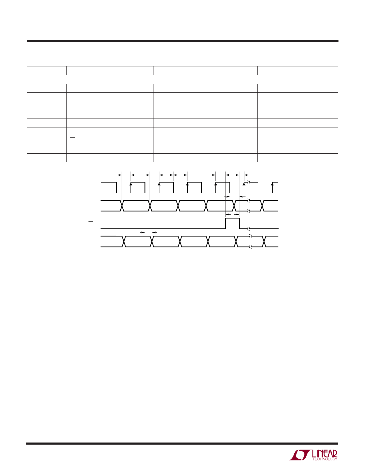
DIN Valid to CLK Setup
DIN Valid to CLK Hold
CLK High
CLK Low
CS/LD Pulse Width
LSB CLK to CS/LD
CS/LD Low to CLK
D
Output Delay CL = 15pF
OUT
CLK Low to CS/LD Low
t
t
1
2
CLK
D
CS/LD
D
OUT
IN
PREVIOUS BYTE CURRENT BYTE
D3 D2 D31 D0 D3
t
8
D3D4 D2 D31 D0 D3
●
30 ns
●
0ns
●
50 ns
●
50 ns
●
40 ns
●
40 ns
●
20 ns
●
●
0ns
t
9
t
5
t
7
D7 • • • D4
D7 • • • D4
6912 TD
t
t
4
3
t
6
85 ns
Note 1: Absolute Maximum Ratings are those values beyond which the life
of the device may be impaired.
Note 2: The LTC6912-1C and LTC6912-1I are guaranteed functional over
the operating temperature range of –40°C to 85°C. The LTC6912-1H is
guaranteed functional over the operating temperature range of –40°C to
125°C.
Note 3: The LTC6912-1C is guaranteed to meet specified performance
from 0°C to 70°C. The LTC6912-1C is designed, characterized and
expected to meet specified performance from – 40°C to 85°C but is not
tested or QA sampled at these temperatures. The LTC6912-1I is
guaranteed to meet specified performance from –40°C to 85°C. The
LTC6912-1H is guaranteed to meet specified performance from –40°C to
125°C.
Note 4: Output voltage swings are measured as differences between the
output and the respective supply rail.
Note 5: Extended operation with output shorted may cause junction
temperature to exceed the 150°C limit for GN package and 125°C for a
DFN package is not recommended.
Note 6: Gain is measured with a large signal DC test using an output
excursion between approximately 30% and 70% of supply voltage.
Note 7: Channel-to-channel isolation is measured by applying a 200kHz
input signal to one channel so that its output varies 1V
, and measuring
RMS
the output voltage RMS of the other channel relative to AGND with its
input tied to AGND. Isolation is calculated:
Isolation
Isolation
= 20 • log10(V
B
= 20 • log10(V
A
OUTA/VOUTB
OUTB/VOUTA
) or
)
High channel-to-channel isolation is strongly dependent on proper circuit
layout. See Applications Information.
Note 8: Offset voltage referred to the INA or INB input is (1 + 1/|GAIN|)
times the offset voltage of the internal op amp, where GAIN is the nominal
gain magnitude. The typical offset voltage values are for 25°C only. See
Applications Information.
Note 9: Input resistance can vary by approximately ±30% part-to-part at a
given gain setting.
Note 10: Guaranteed by design, not subject to test.
Note 11: States 13, 14 and 15 (binary 11xx) are not used. Programming a
channel to states 8 or higher will configure that particular channel into a
low power shutdown state. In addition, programming a channel into
state 15 (binary 1111) will cause that particular channel to draw up to
20mA of supply current and is not recommended.
6912fa
12
UW
TYPICAL PERFOR A CE CHARACTERISTICS
LTC6912
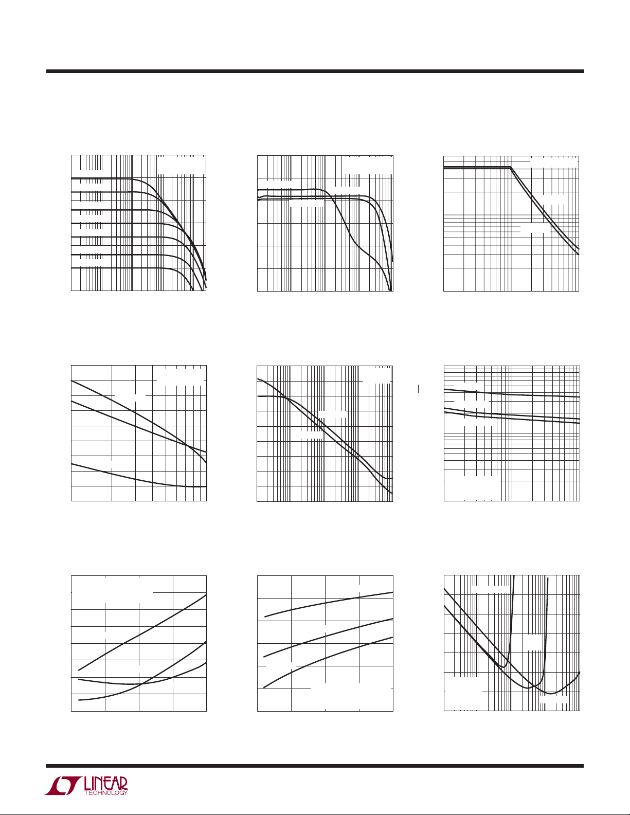
LTC6912-1 Frequency Response
50
GAIN OF 100
40
GAIN OF 50
30
GAIN OF 20
GAIN OF 10
20
GAIN OF 5
GAIN (dB)
10
GAIN OF 2
GAIN OF 1
0
–10
10
1 100 1000 10000
FREQUENCY (kHz)
LTC6912-1 Channel Isolation vs
Frequency
125
120
115
110
105
100
95
90
85
CHANNEL-TO-CHANNEL ISOLATION (dB)
80
100
GAIN OF 10
GAIN OF 1
GAIN OF 100
FREQUENCY (kHz)
VS = ±5V
= 10mV
V
IN
VS = ±5V
= 1V
V
OUT
RMS
6912 G01
RMS
6912 G04
1000
LTC6912-1 Channel Gain
Matching vs Frequency
0.10
0.05
GAIN OF 100
0
–0.05
–0.10
–0.15
CHANNEL-TO-CHANNEL GAIN MATCH (dB)
–0.20
1 100 1000 10000
GAIN OF 10
10
FREQUENCY (Hz)
VS = ±5V
V
IN
GAIN OF 1
LTC6912-1 Power Supply
Rejection vs Frequency
90
80
70
60
50
40
REJECTION (dB)
30
20
10
0
1 100 1000 10000
10
+SUPPLY
–SUPPLY
FREQUENCY (kHz)
LTC6912-1 –3dB Bandwidth vs
Gain Setting
6
= 10mV
RMS
1
VS = 2.7V
–3dB FREQUENCY (MHz)
0.1
1
6912 G02
10 100
GAIN (V/V)
LTC6912-1 Noise Density vs
Frequency
VS = 5V
GAIN = 1
6912 G05 6912 G06
100
GAIN OF 1
GAIN OF 10
GAIN OF 100
10
VS = ±2.5V
VOLTAGE NOISE DENSITY (nV/√HZ)
= 25°C
T
A
INPUT REFERRED
1
1
FREQUENCY (kHz)
10 100
VIN = 10mV
VS = ±5V
RMS
6912 G03
LTC6912-1 Distortion vs
Frequency with Light Loading
–50
RL = 10k
= ±2.5V
V
S
–55
–60
–65
–70
–75
–80
–85
THD-AMPLITUDE BELOW FUNDAMENTAL (dB)
–90
V
0
OUT
= 1V
(2.83)V
RMS
GAIN OF 100
FREQUENCY (kHz)
P-P
GAIN OF 10
GAIN OF 1
15050 100 200
LTC6912-1 Distortion vs
Frequency with Heavy Loading
–30
–40
–50
–60
–70
–80
THD-AMPLITUDE BELOW FUNDAMENTAL (dB)
–90
GAIN OF 1
0
GAIN OF 10
RL = 500Ω
= ±2.5V
V
S
= 1V
V
OUT
50 100 150 200
FREQUENCY (kHz)
GAIN OF 100
(2.83)V
RMS
P-P
LTC6912-1 THD Plus Noise vs
Input Voltage
–30
VS = ±5V
= 10k
R
L
= 1kHz
f
IN
BW = 22kHz
GAIN OF 100
INPUT VOLTAGE (V
GAIN
OF 10
GAIN OF 1
)
P-P
6912fa
–40
–50
–60
–70
–80
THD PLUS NOISE (dB)
–90
–100
0.001 0.1 1 100.01
6912 G08 6912 G096912 G07
13

LTC6912
UW
TYPICAL PERFOR A CE CHARACTERISTICS
LTC6912-1 Hardware Shutdown
Total Supply Current vs
Temperature
HARDWARE SHUTDOWN (GN-16 ONLY)
10
1
TOTAL SUPPLY CURRENT (µA)
0.1
–50 25 75
VS = 2.7V
–25 0
VS = 3V
50 100 125
TEMPERATURE (°C)
LTC6912-1 Gain Shift vs
Temperature (Light Load)
0.10
0.05
0
–0.05
–0.10
GAIN CHANGE (dB)
–0.15
–0.20
GAIN OF 100
VS = 5V
GAIN OF 1
GAIN OF 10
VS = ±5V
6912 G10
VS = 5V
= 10k
R
L
LTC6912-1 Software Shutdown
Total Supply Current vs
Temperature
700
BOTH AMPLIFIERS IN
SOFTWARE SHUTDOWN
= 10k
R
600
L
500
400
300
TOTAL SUPPLY CURRENT (µA)
200
100
–50
–25 0
VS = 2.7V
50 100 125
25 75
TEMPERATURE (°C)
LTC6912-1 Gain Shift vs
Temperature (Heavy Load)
0.5
0
–0.5
GAIN CHANGE (dB)
–1.0
GAIN OF 100
VS = 5V
GAIN OF 1
GAIN OF 10
VS = ±5V
V
= 5V
S
= 500Ω
R
L
6912 G11
LTC6912-1 Total Supply Current
vs Temperature (Both Amplifiers
Active)
5.00
BOTH AMPLIFIERS
PROGRAMMED TO GAIN = 1
4.75
= 10k
R
L
4.50
4.25
4.00
3.75
3.50
TOTAL SUPPLY CURRENT (mA)
3.25
3.00
–50
050
–25 25 75 125
VS = 2.7V
TEMPERATURE (°C)
VS = 5V
LTC6912-2
Frequency Response
40
GAIN OF 64
GAIN OF 32
30
GAIN OF 16
20
GAIN OF 8
GAIN OF 4
GAIN (dB)
10
GAIN OF 2
GAIN OF 1
0
VS = ±5V
VS = ±5V
= 10mV
V
IN
100
6912 G12
RMS
–0.25
–50 25 75
–25 0
TEMPERATURE (°C)
LTC6912-2 Channel Gain
Matching vs Frequency
0.100
0.075
0.050
0.025
GAIN OF 1
GAIN OF 8
0
–0.025
–0.050
–0.075
CHANNEL-TO-CHANNEL GAIN MATCH (dB)
–0.100
GAIN OF 64
1
10 1000
FREQUENCY (kHz)
14
50 100 125
6912 G13
VS = ±5V
= 10mV
V
IN
RL = 10kΩ
100
RMS
6912 G15
10000
–1.5
–50 25 75
–25 0
TEMPERATURE (°C)
50 100 125
LTC6912-2 –3dB Bandwidth vs
Gain Setting
8.0
VS = ±5V
6.0
VS = 2.7V
4.0
2.0
1.0
–3dB FREQUENCY (MHz)
0.8
0.6
0.4
1
10 100
GAIN (V/V)
VIN = 10mV
6912 G14
RMS
6912 G16
–10
1 100 1000 10000
10
FREQUENCY (kHz)
LTC6912-2 Channel Isolation vs
Frequency
125
GAIN = 1
120
115
110
GAIN = 8
105
100
GAIN = 64
95
90
85
CHANNEL-TO-CHANNEL ISOLATION (dB)
80
100
FREQUENCY (kHz)
VS = 5V
V
OUT
= 1V
6912 G14a
RMS
1000
6912 G17
6912fa

UW
TYPICAL PERFOR A CE CHARACTERISTICS
LTC6912-2 Power Supply
Rejection vs Frequency
90
80
70
60
50
40
REJECTION (dB)
30
20
10
0
1
–SUPPLY
10 1000
FREQUENCY (kHz)
+SUPPLY
100
VS = 5V
GAIN = 1
6912 G18
10000
LTC6912-2 Noise Density vs
Frequency
100
VS = ±2.5V
= 25°C
T
A
INPUT REFERRED
10
VOLTAGE NOISE DENSITY (nV/Hz)
1
1
10 100
FREQUENCY (kHz)
GAIN = 1
GAIN = 8
GAIN = 64
6912 G19
LTC6912
LTC6912-2 Distortion vs
Frequency with Light Loading
= 10k)
(R
L
–50
VS = ±2.5V
= 1V
(2.83V
V
OUT
–55
–60
–65
–70
–75
–80
–85
THD (AMPLITUDE BELOW FUNDAMENTAL) (dB)
–90
0
RMS
GAIN = 64
50 100 200
FREQUENCY (kHz)
)
P-P
GAIN = 8
GAIN = 1
150
6912 G20
LTC6912-2 Distortion vs
Frequency with Heavy Loading
(R
= 500Ω)
L
–30
VS = ±2.5V
= 1V
(2.83V
V
OUT
–40
–50
–60
–70
–80
THD (AMPLITUDE BELOW FUNDAMENTAL) (dB)
–90
0
RMS
GAIN = 64
50 100 150 200
FREQUENCY (kHz)
P-P
GAIN = 8
)
GAIN = 1
LTC6912-2 Software Shutdown
Total Supply Current vs
Temperature
800
BOTH AMPLIFIERS
PROGRAMMED TO STATE = 8
700
= 10k
R
L
600
500
400
300
TOTAL SUPPLY CURRENT (A)
200
100
–50
–25 0
50 100 125
25 75
TEMPERATURE (°C)
VS = 5V
VS = 2.7V
6912 G21
VS = 5V
6912 G23
LTC6912-2 THD + Noise vs
Input Voltage
–30
–40
–50
–60
–70
THD + NOISE (dB)
–80
VS = 5V
–90
= 10k
R
L
= 1kHz
f
IN
–100
0.001 0.1 1 10
GAIN = 64
0.01
INPUT VOLTAGE (V
GAIN = 8
P-P
)
LTC6912-2 Total Supply Current
vs Temperature (Both Amplifiers
Active)
6.0
BOTH AMPLIFIERS
ACTIVE : GAIN = 1
5.5
= 10k
R
L
5.0
4.5
4.0
TOTAL SUPPLY CURRENT (mA)
3.5
3.0
–50
–25 0
TEMPERATURE (°C)
50 100 125
25 75
GAIN = 1
6912 G22
VS = ±5V
VS = 5V
VS = 2.7V
6912 G24
LTC6912-2 Hardware Shutdown
Total Supply Current vs
Temperature
HARDWARE SHUTDOWN (GN-16 ONLY)
10
1
TOTAL SUPPLY CURRENT (µA)
0.1
–50 25 75
VS = 2.7V
–25 0
VS = 3V
TEMPERATURE (°C)
LTC6912-2 Gain Shift vs
Temperature (Light Load)
0.100
0.075
0.050
0.025
0
–0.025
–0.050
–0.075
–0.100
GAIN CHANGE (dB)
–0.125
–0.150
–0.175
–0.200
–50 25 75
–25 0
TEMPERATURE (°C)
VS = ±5V
VS = 5V
50 100 125
6912 G22A
VS = 5V
= 10k
R
L
GAIN = 1
GAIN = 8
GAIN = 64
50 100 125
6912 G25
6912fa
15

LTC6912
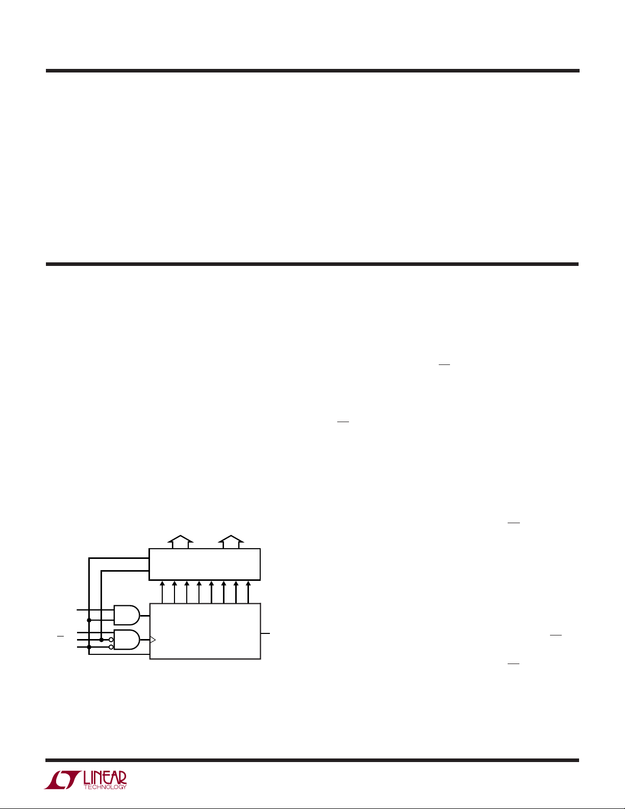
+
–
+
–
MOS INPUT
OP AMP
MOS INPUT
OP AMP
V
+
V
+
V
–
SHDN
CS/LD
DATA
CLK
6912 BD
LOWER
NIBBLE
UPPER
NIBBLE
8-BIT
LATCH
8-BIT
SHIFT-REGISTER
INPUT R ARRAY
FEEDBACK R ARRAY
INPUT R ARRAY
FEEDBACK R ARRAY
CHANNEL A CHANNEL B
Q0 Q1 Q2 Q3 Q4 Q5 Q6 Q7
5
3
1 16
15
13
14
12
10
11
6
7
8
9
2
4
NC
INA
AGND
V
–
OUT A
OUT B
NC
V
+
NC
DGND
D
OUT
INB
100k
100k
UW
TYPICAL PERFOR A CE CHARACTERISTICS
LTC6912-2 Gain Shift vs
Temperature (Heavy Load)
0.25
–0.25
0
GAIN = 1
VS = 5V
R
GAIN = 8
= 500
L
U
UU
PI FU CTIO S
INA, INB: Analog Inputs. The input signal to the A channel
amplifier of the LTC6912-X is the voltage difference between the INA pin and AGND pin. Likewise, the input signal
to the B channel amplifier of the LTC6912-X is the voltage
difference between the INB pin and AGND pin. The INA (or
INB) pin connects internally to a digitally controlled resistance whose other end is a current summing point at the
same potential as the AGND pin (Figure 1). At unity gain,
the value of this input resistance is approximately 10kΩ
and the INA (or INB) pin voltage range is rail-to-rail (V+ to
V–). At gain settings above unity, the input resistance falls.
The linear input range at INA and INB also falls inversely
proportional to the programmed gain. Tables 1 and 2
summarize this behavior. The higher gains are designed to
boost lower level signals with good noise performance. In
the “zero” gain state (state = 0), or in software shutdown
(state = 8) analog switches disconnect the INA or INB pin
internally and this pin presents a very high input resistance. In the “zero” gain state (state = 0), the input may
vary from rail to rail but the output is insensitive to it and
is forced to the AGND potential. Circuitry driving the INA
and INB pins must consider the LTC6912-X’s input resistance, its process variance, and the variation of this
resistance from gain setting to gain setting. Signal sources
with significant output resistance may introduce a gain
error as the source’s output resistance and the LTC6912X’s input resistance forms a voltage divider. This is especially true at higher gain settings where the input resistance is the lowest.
16
–0.50
GAIN CHANGE (dB)
–0.75
–1.00
–50 25 75
–25 0
GAIN = 64
50 100 125
TEMPERATURE (°C)
6912 G26
In single supply voltage applications, the LTC6912-X’s DC
ground reference for both input and output is AGND, not
V–. With increasing gains, the LTC6912-X’s input voltage
range for an unclipped output is no longer rail-to-rail but
diminishes inversely to gain, centered about the AGND
potential.
Figure 1. GN-16 Block Diagram
6912fa

LTC6912
U
UU
PI FU CTIO S
AGND: Analog Ground. The AGND pin is at the midpoint of
an internal resistive voltage divider, developing a potential
halfway between the V
the AGND pin has an equivalent input resistance of nominally 50k (Figure 1). In order to reduce the quiescent
supply current in hardware shutdown (SHDN pin pulled to
+
V
, GN-16 only), the equivalent series resistance of this
pin significantly increases (to a value on the order of
800kΩ with 5V supplies, but is highly supply voltage,
temperature, and process dependent). AGND is the
noninverting input to both the internal channel A and
channel B amplifiers. This makes AGND the ground reference voltage for the INA, INB, OUTA, and OUTB pins.
Recommended analog ground plane connection depends
on how power is applied to the LTC6912-X (See Figures 2,
3, and 4). Single power supply applications typically use
V– for the system signal ground. The analog ground plane
in single-supply applications should therefore tie to V
and the AGND pin should be bypassed to this ground plane
by a high quality capacitor of at least 0.1µF (Figure 2). The
AGND pin provides an internal analog reference voltage at
half the V
+
supply voltage. Dual supply applications with
symmetrical supplies (such as ±5V) have a natural system
ground plane potential of zero volts, in which the AGND pin
can be directly tied to, making the zero volt ground plane
the input and output reference voltage for the LTC6912-X
(Figure 3). Finally, if dual asymmetrical power supplies are
used, the supply ground is still the natural ground plane
voltage. To maximize signal swing capability with an
+
and V– pins. In normal operation,
–
,
asymmetrical supply, however, it is often desirable to refer
the LTC6912-X’s analog input and output to a voltage
+
equidistant from the two supply rails V
and V–. The AGND
pin will provide such a potential when open-circuited and
bypassed with a capacitor (Figure 4). In noise sensitive
applications where AGND does not tie directly to a ground
plane, as in Figures 2 and 4, it is important to AC-bypass
the AGND pin. Otherwise channel to channel isolation is
degraded, and wideband noise will enter the signal path
from the thermal noise of the internal voltage divider
resistors which present a Thévenin equivalent resistance
of approximately 50kΩ. This noise can reduce SNR by at
least 15dB at high gain settings. An external capacitor
from AGND to the ground plane, whose impedance is well
below 50kΩ at frequencies of interest, will filter and
suppress this noise. A 0.1µF high quality capacitor is
effective for frequencies down to 1kHz. Larger capacitors
will extend this suppression to lower frequencies. This
issue does not arise in dual supply applications because
the AGND pin ties directly to ground. In applications
requiring an analog ground reference other than half the
total supply voltage, the user can override the built-in
analog ground reference by tying the AGND pin to a
reference voltage with the AGND voltage range specified in
the Electrical Characteristics Table. The AGND pin will load
the external reference with approximately 50kΩ returned
to the half-supply potential. AGND should still be capacitively bypassed to a ground plane as noted above. Do not
connect the AGND pin to the V
–
pin.
+
V
REFERENCE
2
≥0.1µF
SERIAL
INTERFACE
1
2
3
4
5
6
7
8
LTC6912-X
ANALOG GROUND PLANE
16
15
14
13
12
11
10
9
DIGITAL GROUND PLANE
0.1µF
V
+
6912 F02
SINGLE-POINT
SYSTEM GND
Figure 2. Single Supply Ground Plane Connection
ANALOG GROUND PLANE
SERIAL
INTERFACE
1
2
3
4
5
6
7
8
LTC6912-X
16
15
0.1µF
–
V
14
13
0.1µF
+
V
12
11
10
9
DIGITAL GROUND PLANE
6912 F03
SINGLE-POINT
SYSTEM GND
Figure 3. Symmetrical Dual Supply Ground Plane Connection
6912fa
17

LTC6912
U
UU
PI FU CTIO S
+ + V–
V
REFERENCE
2
≥0.1µF
SERIAL
INTERFACE
Figure 4. Asymmetrical Dual Supply Ground Plane Connection
1
2
3
4
5
6
7
8
LTC6912-X
SHDN (GN-16 ONLY): CMOS Compatible Logic Hardware
Shutdown Input. The LTC6912-X has two shutdown modes.
One is a software shutdown state which can be software
programmed into either Channel A, Channel B, or both.
The software shutdown, when programmed to a particular
channel (state = 8), will disable that channel’s amplifier
and tri-state open its analog input and analog output. The
serial interface, however is still active. A hardware shutdown occurs when the SHDN pin is pulled to the positive
rail. In this condition, both amplifiers and serial interface
are disabled. The SHDN pin is allowed to swing from V
10.5V above V
–
, regardless of V+ so long as the logic levels
meet the minimum requirements specified in the Electrical
Characteristics table. The SHDN pin is a high impedance
CMOS logic input, but has a small pull-down current
source (<10µA) which will force SHDN low if the logic
input is externally floated. On initial power up (with SHDN
open), or coming out of the hardware shutdown mode
(pulling SHDN to V
–
power-on reset state (software shutdown mode, state = 8)
for both channels.
CS/LD: TTL/CMOS Compatible Logic Input. When this pin
is asserted low, the CLK pin is enabled, and the 8-bit shift
register serially shifts the shift register contents and
whatever data is present on the DIN pin into the shift
register on the rising edge of CLK. On the rising edge of
CS/LD, the contents of the shift register data are loaded
into the eight bit latch which configures the gain state of
both channel A and channel B amplifiers. A logic high on
CS/LD inhibits the CLK signal internally to the IC.
ANALOG GROUND PLANE
16
15
0.1µF
–
V
14
13
0.1µF
+
V
12
11
10
9
DIGITAL GROUND PLANE
6912 F04
SINGLE-POINT
SYSTEM GND
–
to
), both amplifiers are reset into the
: TTL/CMOS Compatible Logic Serial Data Input. The
D
IN
serial interface is synchronously loaded MSB first via D
IN
on the rising edge of CLK with CS/LD asserted low.
CLK: TTL/CMOS Compatible Logic Input. With CS/LD
asserted low, the clock synchronizes the loading of the
serial shift register on its rising and falling edges. Data is
shifted in at D
on D
D
on the falling edge of CLK.
OUT
: TTL/CMOS Compatible Logic Output. The MSB of
OUT
the shift register contents is shifted out at D
falling edge of CLK. The output at D
on the rising edge of CLK and is shifted out
IN
on the
OUT
swings between V
OUT
+
and DGND, and is rated to drive approximately 15pF.
DGND: Digital Ground: The DGND pin defines the potential
from which LOGIC levels V
and VIL for the 3-wire serial
IH
digital interface are referenced. The recommended connection of DGND depends on how power is applied to the
LTC6912 (See Figures 2, 3, and 4). (CAVEAT: Under no
conditions is DGND to exceed either supply pins V
–
, which could result in damage to the IC if not current
V
+
and
limited.)
Single power supply applications typically use V
–
for the
system signal ground. The preferred connection for DGND
–
is therefore V
(See Figure 2).
Dual supply applications with symmetrical supplies (such
as ±5V) have a natural system ground potential of zero
volts, in which the DGND pin can be tied to, making the
zero volt ground plane the logic reference (Figure 3).
Finally, if dual asymmetrical power supplies are used, the
system ground is still the natural ground plane voltage.
–
, V+: Power Supply Pins. The V+ and V– pins should be
V
bypassed with 0.1µF capacitors to an adequate analog
ground plane using the shortest possible wiring. Electrically clean supplies and a low impedance ground are
important for the high dynamic range available from the
LTC6912 (see further details under the AGND pin description). Low noise linear power supplies are recommended.
Switching power supplies require special care to prevent
switching noise coupling into the signal path, reducing
dynamic range.
18
6912fa
LTC6912
U
UU
PI FU CTIO S
OUT A, OUT B: Analog Output. These pins are the output
of the A and B channel amplifiers respectively. Each
+
operational amplifier can swing rail-to-rail (V
to V–) as
specified in the Electrical Characteristics table. For best
performance, loading the output as lightly as possible will
minimize signal distortion and gain error. The Electrical
Characteristics table shows performance at output currents up to 10mA, and the current limits which occur when
the output is shorted midsupply at 2.7V and ±5V supplies.
U
WUU
APPLICATIO S I FOR ATIO
Functional Description
The LTC6912-X is a small outline, wideband, inverting
two-channel amplifier with voltage gains that are independently programmable. Each delivers a choice of eight
voltage gains, configurable through a 3-wire serial digital
interface, which accepts TTL or CMOS logic levels (See
Figure 5). Tables 1 and 2 list the nominal gains for the
LTC6912-1 and LTC6912-2 respectively. Gain control
within the amplifier occurs by switching resistors from a
matched array in or out of a closed-loop op amp circuit
using MOS analog switches (Figure 1). The bandwidths of
the individual amplifiers depend on gain setting. The
Typical Performance Characteristics section shows measured frequency responses.
CHANNEL A CHANNEL B
RESET
LE
D
IN
CLK
CS/LD
SHDN
Figure 5. Serial Digital Interface Block Diagram
LSB MSB
RESET
8-BIT LATCH
LOWER NIBBLE
Q0 Q1 Q2 Q3 Q4 Q5 Q6 Q7
UPPER NIBBLE
8-BIT
SHIFT-REGISTER
D
OUT
6912 F05
Output current above 10mA is possible but current-limiting circuitry will begin to affect amplifier performance at
approximately 20mA. Long-term operation above 20mA
output is not recommended. Do not exceed maximum
junction temperature of 150°C for a GN and 125°C for a
DFN package. The output will drive capacitive loads up to
50pF. Capacitances higher than 50pF should be isolated
by a series resistor (10Ω or higher).
Description of the 3-Wire SPI Interface
Gain control of each amplifier is independently programmable using the 3-wire SPI interface (see Figure 5). Logic
levels for the LTC6912 3-wire serial interface are TTL/
CMOS compatible. When CS/LD is low, the serial data on
D
is shifted into an 8-bit shift-register on the rising edge
IN
of the clock, with the MSB transferred first. Serial data on
is shifted out on the clock’s falling edge. A rising edge
D
OUT
on CS/LD will latch the shift-register’s contents into an 8bit D-latch and disable the clock internally on the IC. The
upper nibble of the D-latch (4 most significant bits),
configure the gain for the B-channel amplifier. The lower
nibble of the D-latch (4 least significant bits), configures
the gain for the A-channel amplifier. Tables 1 and 2 detail
the nominal gains and respective gain codes. Care must be
taken to ensure CLK is taken low before CS/LD is pulled
low to avoid an extra internal clock pulse to the input of the
8-bit shift-register (See Figure 5).
D
is active in all states, therefore D
OUT
cannot be
OUT
“wire-OR’d” to other SPI outputs.
An LTC6912 may be daisy-chained with other LTC6912s
or other devices having serial interfaces by connecting the
to the DIN of the next chip while CLK and CS/LD
D
OUT
remain common to all chips in the daisy chain. The serial
data is clocked to all the chips then the CS/LD signal is
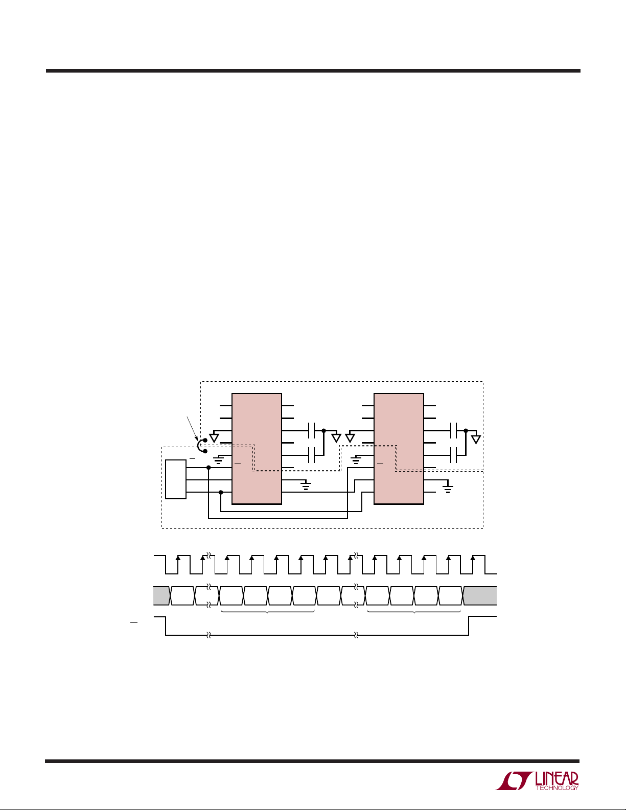
pulled high to update all of them simultaneously. Figure 6
shows an example of two LTC6912s in a daisy chained SPI
6912fa
19
LTC6912
WUUU
APPLICATIO S I FOR ATIO
configuration. It is recommended the serial interface signals should remain idle in between data transfers in order
to minimize digital noise coupling into the analog path.
Power On Reset
On the initial application of power, the power on reset
state of both amplifiers is low power software shutdown
(state = 8) (see Tables 1 and 2). In this state, both analog
amplifiers are disabled and have their inputs and outputs
opened. This will facilitate the application of using the
device as a 2:1 analog MUX, in that the amplifier’s outputs
may be wired-OR together and the LTC6912 can alternately select between A and B channels. Care must be
taken if the outputs are wired-OR’d to ensure the software
shutdown state (state = 8) is always programmed in one
of the two channels.
SINGLE-POINT
SYSTEM GND
µP
CS/LD
DATA
CLK
1
2
3
4
5
6
7
8
LTC6912-X
SHDN
CS/LD
D
IN
DGND
D
OUT
16
15
0.1µF
–
V
14
13
0.1µF
+
V
12
11
10
9
Timing Constraints
Settling time in the CMOS gain-control logic is typically
several nanoseconds and is faster than the analog signal
path. When the amplifier gain changes, the limiting timing
is analog. As with any programmable-gain amplifier, each
gain change causes an output transient as the amplifier’s
output moves, with finite speed, toward a differently
scaled version of the input signal. The LTC6912-X analog
path settles with a characteristic time constant or time
scale, τ, that is roughly the standard value for a first order
band limited response:
τ = 0.35/f
–3dB
See the –3dB BW vs Gain Setting graph in the Typical
Performance Characteristics section.
ANALOG GROUND PLANE
1
2
3
4
5
6
7
8
LTC6912-X
SHDN
CS/LD
D
IN
DGND
D
OUT
16
15
0.1µF
–
V
14
13
0.1µF
+
V
12
11
10
9
20
CLK
D
CS/LD
DIGITAL GROUND PLANE
IN
D15 D11 D10 D9 D8 D7 D3 D2 D1 D0
6912 F06
Figure 6. Two LTC6912s (Four PGAs) in Daisy Chain Configuration
6912fa

WUUU
APPLICATIO S I FOR ATIO
LTC6912
Offset Voltage vs Gain Setting
The electrical tables list DC offset (error), V
inputs of the internal op amp (See Figure 1). The electrical
tables also show the resulting, gain dependent offset
voltage referred to the INA, or INB pins, V
measures are related through the feedback/input resistor
ratio, which equals the nominal gain-magnitude setting,
|GAIN|:
V
Offset voltages at any gain setting can be inferred from this
relationship. For example, an internal amplifier offset
V
OS(OA)
2mV at a gain setting of 1, or 1.5mV at a gain setting of 2.
At high gains, V
is random and can have either polarity centered on 0V).
The MOS input circuitry of the internal op amp in Figure 1
draws negligible input currents (less than 10µA), so only
V
OS(OA)
AC-Coupled Operation
Adding capacitors in series with the INA and INB pins
converts the LTC6912-X into a dual AC-coupled inverting
amplifier, suppressing the input signal’s DC level (and also
adding the additional benefit of reducing the offset voltage
from the LTC6912-X’s amplifier itself). No further components are required because the input of the LTC6912-X
biases itself correctly when a series capacitor is added.
The INA and INB analog input pins connect internally to a
resistor whose nominal value varies between 10kΩ and
1kΩ depending on the version of LTC6912 used (see the
rightmost column of Tables 1 and 2). Therefore, the low
frequency cutoff will vary with capacitor and gain setting.
If, for example, a low frequency corner of 1kHz (or lower)
on the LTC6912-1 is desired, use a series capacitor of
0.16µF or larger. 0.16µF has a reactance of 1kΩ at 1kHz,
giving a 1kHz lower –3dB frequency for gain settings of
10V/V through 100V/V. If the LTC6912-1 is operated at
lower gain settings with a 0.16µF capacitor, the higher
input resistance will reduce the lower corner frequency
down to 100Hz at a gain setting of 1V/V. These frequencies
scale inversely with the value of input capacitor used.
= (1 + 1/|GAIN|) V
OS(IN)
of 1mV will appear referred to the INA, INB pins as
approaches V
OS(IN)
and the GAIN affect the overall amplifier’s offset.
OS(OA)
OS(OA)
OS(IN)
. (Offset voltage
OS(OA)
. The two
, at the
Note that operating the LTC6912 family in “zero” gain
mode (digital state 0000) open circuits both the INA and
INB pins and this demands some care if employed with a
series AC coupling input capacitor. When the chip enters
the zero gain mode, the opened INA or INB pin tends to
sample and freeze the voltage across the capacitor to the
value it held just before the zero gain state. This can place
the INA or INB pin at or near the DC potential of a supply
rail. (The INA or INB pin may also drift to a supply potential
in this state due to small leakage currents.) To prevent
driving the INA or INB pin outside the supply limit and
potentially damaging the chip, avoid AC input signals in
the zero gain state with an AC coupling capacitor. Also,
switching later to a non-zero gain value will cause a
transient pulse at the output of the LTC6912-1 (with a time
constant set by the capacitor value and the new LTC6912-1
input resistance value). This occurs because the INA and
INB pins return to the AGND potential forcing transient
current sourced by the amplifier output to charge the AC
coupling capacitor to its proper DC blocking value.
SNR and Dynamic Range
The term “dynamic range” is much used (and abused)
with signal paths. Signal-to-noise (SNR) is an unambiguous comparison of signal and noise levels, measured in
the same way and under the same operating conditions. In
a variable gain amplifier, however, further characterization
is useful because both noise and maximum signal level in
the amplifier will vary with the gain setting, in general. In
the LTC6912-X, maximum output signal is independent of
gain (and is near the full power supply voltage, as detailed
in the swing sections of the Electrical Characteristics
table). The maximum input level falls with increasing gain,
and the input-referred noise falls as well (listed also in the
table). To summarize the useful signal range in such an
amplifier, we define dynamic range (DR) as the ratio of
maximum input (at unity gain) to minimum input-referred
noise (at maximum gain). This DR has a physical interpretation as the range of signal levels that will experience an
SNR above unity V/V or 0dB. At a 10V total power supply,
DR in the LTC6912-X (gains 0V/V to 100V/V), the DR is
typically 115dB (the ratio of 9.9 V
mum input to the 6.3µV
RMS
P-P
high gain input noise). The
, or 3.5V
RMS
, maxi-
6912fa
21

LTC6912
WUUU
APPLICATIO S I FOR ATIO
SNR from an amplifier is the ratio of input level to inputreferred noise, and can be 108dB with the LTC6912 family
at unity gain.
Construction and Instrumentation Cautions
Electrically clean construction is important in applications
seeking the full dynamic range of the LTC6912 family of
dual amplifiers. It is absolutely critical to have AGND either
AC bypassed or wired directly using the shortest possible
wiring, to a low impedance ground return for best channelto-channel isolation. Short, direct wiring minimizes parasitic capacitance and inductance. High quality supply
bypass capacitors of 0.1µF near the chip provide good
U
TYPICAL APPLICATIO
Low Noise AC Amplifier with Programmable Gain and
Bandwidth
Analog data acquisition can exploit band limiting as well as
gain to suppress unwanted signals or noise. Tailoring an
analog front end to both the level and bandwidth of each
source maximizes the resulting SNR. Figure 7 shows a
block diagram for a low noise amplifier with gain and
bandwidth independently programmable over a 100:1
range. Channels A and B of the LTC6912-1 are used to
independently control the gain and bandwidth respectively over a 100:1 range. The LT1884 dual op amp forms
decoupling from a clean, low inductance power source.
But several centimeters of wire (i.e., a few µH of induc-
tance) from the power supplies, unless decoupled by
substantial capacitance (>10µF) near the chip, can create
a parasitic high-Q LC resonant circuit in the hundreds of
kHz range in the chip’s supplies or ground reference. This
may impair circuit performance at those frequencies. A
compact, carefully laid out printed circuit board with a
good ground plane makes a significant difference in minimizing distortion. Finally, equipment to measure performance can itself introduce distortion or noise floors.
Checking for these limits with wired shorts from INA to
OUTA and INB to OUTB in place of the chip is a prudent
routine procedure.
an integrating lowpass loop with capacitor C2 to set the
programmable upper corner frequency. The LT1884 also
supports rail-to-rail output swings over the total supply
voltage range of 2.7V to 10.5V. AC coupling through
capacitor C1 establishes a fixed low frequency corner of
1Hz, which can be adjusted by changing C1. Alternatively,
shorting C1 makes the amplifier DC coupled. If DC gain is
not needed, the AC coupling cap C1 serves to suppress
several error sources: any shift in DC levels, low frequency
noise, and DC offset voltages (not including the LT1884’s
low internal offset).
22
CONTROL
V
IN
GAINA
INA OUTA
LTC6912-1
CHANNEL A
= GAINA V
V
OUT
Figure 7. Block Diagram of an AC Amplifier with Programmable Gain and Bandwidth
GAIN
PGA
R2
15.8k
C2
1µF
C1
R1
10µF
15.8k
R2
IN
R1
–3dB BANDWIDTH RANGE IS FROM TO ≤
1M
–
1/2 LT1884
+
BANDWIDTH
CONTROL
PGA
GAINB
INB OUTB
LTC6912-1
CHANNEL B
1
2πR1C1
2π
(
GAINB
R
1
R2
)
C2
R
–
1/2 LT1884
+
1/2 LT1884
V
OUT
6912 F07
6912fa

PACKAGE DESCRIPTIO
LTC6912
U
DE/UE Package
12-Lead Plastic DFN (4mm × 3mm)
(Reference LTC DWG # 05-08-1695)
3.50 ±0.05
0.65 ±0.05
1.70 ±0.05
(2 SIDES)2.20 ±0.05
0.25 ± 0.05
RECOMMENDED SOLDER PAD PITCH AND DIMENSIONS
NOTE:
1. DRAWING PROPOSED TO BE A VARIATION OF VERSION
(WGED) IN JEDEC PACKAGE OUTLINE M0-229
2. DRAWING NOT TO SCALE
3. ALL DIMENSIONS ARE IN MILLIMETERS
3.30 ±0.05
(2 SIDES)
0.50
BSC
4.00 ±0.10
(2 SIDES)
PIN 1
TOP MARK
PACKAGE OUTLINE
(NOTE 6)
0.200 REF
4. DIMENSIONS OF EXPOSED PAD ON BOTTOM OF PACKAGE DO NOT INCLUDE
MOLD FLASH. MOLD FLASH, IF PRESENT, SHALL NOT EXCEED 0.15mm ON ANY SIDE
5. EXPOSED PAD SHALL BE SOLDER PLATED
6. SHADED AREA IS ONLY A REFERENCE FOR PIN 1 LOCATION
ON THE TOP AND BOTTOM OF PACKAGE
GN Package
16-Lead Plastic SSOP (Narrow .150 Inch)
(Reference LTC DWG # 05-08-1641)
.045 ±.005
16
3.00 ±0.10
0.75 ±0.05
.189 – .196*
(4.801 – 4.978)
15
14
13
(2 SIDES)
12 11 10
R = 0.20
TYP
1.70 ± 0.10
(2 SIDES)
0.00 – 0.05
9
R = 0.115
TYP
0.25 ± 0.05
3.30 ±0.10
(2 SIDES)
BOTTOM VIEW—EXPOSED PAD
.009
(0.229)
REF
0.50
BSC
127
16
0.38 ± 0.10
PIN 1
NOTCH
(UE12/DE12) DFN 0603
.254 MIN
RECOMMENDED SOLDER PAD LAYOUT
.007 – .0098
(0.178 – 0.249)
.016 – .050
NOTE:
1. CONTROLLING DIMENSION: INCHES
2. DIMENSIONS ARE IN
3. DRAWING NOT TO SCALE
*DIMENSION DOES NOT INCLUDE MOLD FLASH. MOLD FLASH
SHALL NOT EXCEED 0.006" (0.152mm) PER SIDE
**DIMENSION DOES NOT INCLUDE INTERLEAD FLASH. INTERLEAD
FLASH SHALL NOT EXCEED 0.010" (0.254mm) PER SIDE
(0.406 – 1.270)
(MILLIMETERS)
INCHES
.150 – .165
.0250 BSC.0165 ± .0015
.015
(0.38 ± 0.10)
0° – 8° TYP
± .004
Information furnished by Linear Technology Corporation is believed to be accurate and reliable.
However, no responsibility is assumed for its use. Linear Technology Corporation makes no representation that the interconnection of its circuits as described herein will not infringe on existing patent rights.
× 45°
.229 – .244
(5.817 – 6.198)
.0532 – .0688
(1.35 – 1.75)
.008 – .012
(0.203 – 0.305)
TYP
12
.150 – .157**
(3.810 – 3.988)
5
4
678
3
.004 – .0098
(0.102 – 0.249)
.0250
(0.635)
GN16 (SSOP) 0204
BSC
6912fa
23

LTC6912
TYPICAL APPLICATIO
U
A 2:1 PGA MUX
+
V
V
0.1µF
12 14
+
–
V
2
1µF
CLK
INA
3
AGND
4
INB
5
SHDN
6
CS/LD
7
D
8
LTC6912-X
CHB CHA
IN
DGND
D
CHANNEL A
INPUT
CHANNEL B
INPUT
SHDN
3-WIRE
INTERFACE
MUX OPERATION: IF THE LOWER NIBBLE (Q3, Q2, Q1, Q0) IS (1, 0, 0, 0) THEN OUTA IS IN
TRI-STATE AND THE UPPER NIBBLE (Q7, Q6, Q5, Q4) CONTROLS THE ACTIVE CHANNEL B.
CS/LD
DATA
SPI
IF THE UPPER NIBBLE IS (1, 0, 0, 0) THEN OUTB IS IN TRI-STATE
AND THE LOWER NIBBLE CONTROLS ACTIVE CHANNEL A.
OUT A
OUT B
OUT
15
13
10
9
V
OUT
(TO ADC)
6912 TA02
RELATED PARTS
PART NUMBER DESCRIPTION COMMENTS
LT1228 100MHZ Gain Controlled Transconductance Amplifier Differential Input, Continuous Analog Gain Control
LT1251/LT1256 40Mhz Video Fader and Gain Controlled Amplifier Two Input, One Output, Continuous Analog Gain Control
LTC1564 10kHz to 150kHz Digitally Controlled Filter and PGA Continuous Time, Low Noise 8th Order Filter and 4-Bit PGA
LTC6910-1/-2/-3 Digitally Controlled Programmable Gain Amplifier Single Programmable Gain Amplifier, 3-Bit Parallel Digital Interface
in SOT-23
LTC6911-1/-2 Dual Digitally Controlled Programmable Gain Amplifier Dual Programmable Gain Amplifiers, 3-Bit Parallel Digital Interface
in MSOP-10
LTC6915 Zero Drift Instrumentation Amp Gains 0 - 4096V/V, 116dB CMRR
with Digitally Programmable Gain
24
Linear Technology Corporation
1630 McCarthy Blvd., Milpitas, CA 95035-7417
(408) 432-1900 ● FAX: (408) 434-0507 ● www.linear.com
6912fa
LT/LT 1005 REV A • PRINTED IN USA
© LINEAR TECHNOLOGY CORPORATION 2004
 Loading...