

Linear Technology LTC6908CS6-2, LTC6908 Datasheet
LTC6908-1/LTC6908-2
1
690812fa
690812 TA01b
FREQUENCY
(FUNDAMENTAL AND HARMONICS SHOWN)
150kHz
0
–10
–20
–30
–40
0
–10
–20
–30
–40
OUTPUT (dBc) OUTPUT (dBc)
30MHz
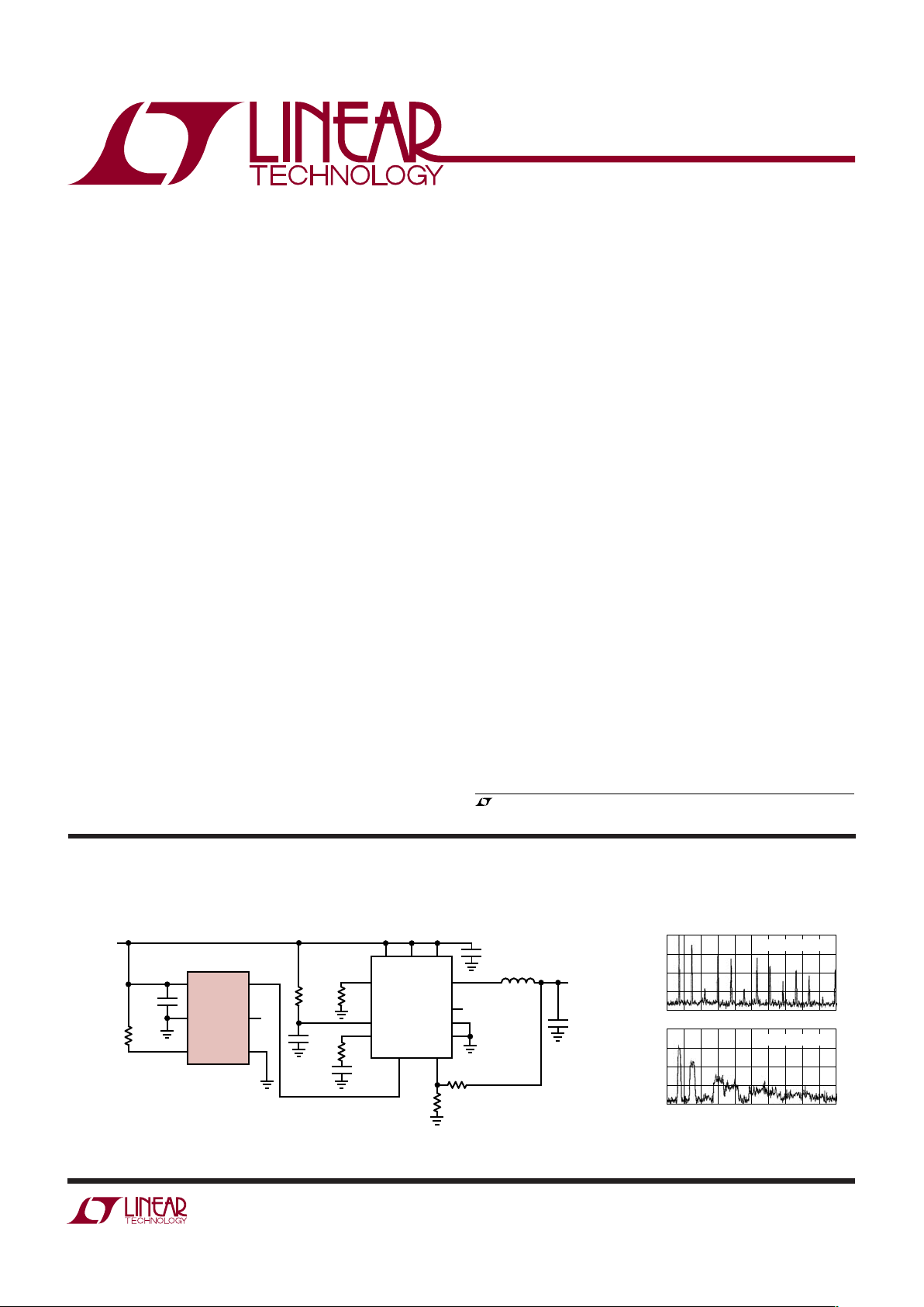
SSFM DISABLED
SSFM ENABLED
Resistor Set SOT-23
Oscillator with Spread
Spectrum Modulation
The LTC®6908 is an easy-to-use precision oscillator that
provides 2-outputs, shifted by either 180° or 90°. The
oscillator frequency is programmed by a single external
resistor (R
SET
) and spread spectrum frequency modulation
(SSFM) can be activated for improved electromagnetic
compatibility (EMC) performance.
The LTC6908 operates with a single 2.7V to 5.5V supply
and provides rail-to-rail, 50% duty cycle square wave
outputs. A single resistor from 10k to 2M is used to select
an oscillator frequency from 50kHz to 10MHz (5V supply).
The oscillator can be easily programmed using the simple
formula outlined below:
f
OUT
=10MHz • 10k/R
SET
The LTC6908’s SSFM capability modulates the output
frequency by a pseudorandom noise (PRN) signal to
decrease the peak electromagnetic radiation level and
improve EMC performance. The amount of frequency
spreading is fi xed at ±10% of the center frequency. When
SSFM is enabled, the rate of modulation is selected by the
user. The three possible modulation rates are f
OUT
/16,
f
OUT
/32 and f
OUT
/64.
■
Switching Power Supply Clock Reference
■
Portable and Battery-Powered Equipment
■
Precision Programmable Oscillator
■
Charge Pump Driver
■
LTC6908-1: Complementary Outputs (0°/180°)
■
LTC6908-2: Quadrature Outputs (0°/90°)
■
50kHz to 10MHz Frequency Range
■
One External Resistor Sets the Frequency
■
Optional Spread Spectrum Frequency Modulation
for Improved EMC Performance
■
±10% Frequency Spreading
■
400µA Supply Current Typical (V+ = 5V, 50kHz)
■
Frequency Error ≤1.5% Max (TA = 25°C, V+ = 3V)
■
±40ppm/°C Temperature Stability
■
Fast Start-Up Time: 260µs Typical (1MHz)
■
Outputs Muted Until Stable
■
Operates from a Single 2.7V to 5.5V Supply
■
Available in Low Profi le (1mm) ThinSOT and DFN
(2mm × 3mm) Packages
APPLICATIO S
U
FEATURES
DESCRIPTIO
U
, LT, LTC and LTM are registered trademarks of Linear Technology Corporation.
All other trademarks are the property of their respective owners.
2.25MHz, 2.5V/8A Step-Down Regulator
TYPICAL APPLICATIO
U
C
BYP
44.2k
OUT1
OUT2
f
OUT
= 10MHz • 10k/R
SET
MOD
V
+
GND
SET
690812 TA01a
SVINTRACK
LTC3418
R
T
C
IN
100µF
0.2µH
LTC6908-1
RUN/SS
I
TH
PGOOD
SW
PGND
SGND
SYNC/MODE V
FB
PV
IN
820pF
1000pF
0.1µF
C
OUT
100µF
×2
V
OUT
2.5V
8A
4.32k
2k
41.2k
2.2M
V
IN
2.8V TO 5.5V
4.99k
150kHz to 30MHz Output
Frequency Spectrum
(9kHz Res BW)
LTC6908-1/LTC6908-2
2
690812fa
Total Supply Voltage (V+ to GND) ...............................6V
Maximum Voltage on any Pin
(GND – 0.3V) ≤ V
PIN
≤ (V+ + 0.3V)
Output Short Circuit Duration .......................... Indefi nite
Operating Temperature Range (Note 2)
LTC6908CS6-1/LTC6908CS6-2 ............ –40°C to 85°C
LTC6908IS6-1/LTC6908IS6-2 .............. –40°C to 85°C
LTC6908HS6-1/LTC6908HS6-2 .........–40°C to 125°C
LTC6908CDCB-1/LTC6908CDCB-2 ......–40°C to 85°C
LTC6908IDCB-1/LTC6908IDCB-2 ......... –40°C to 85°C
(Note 1)
ABSOLUTE AXI U RATI GS
W
WW
U
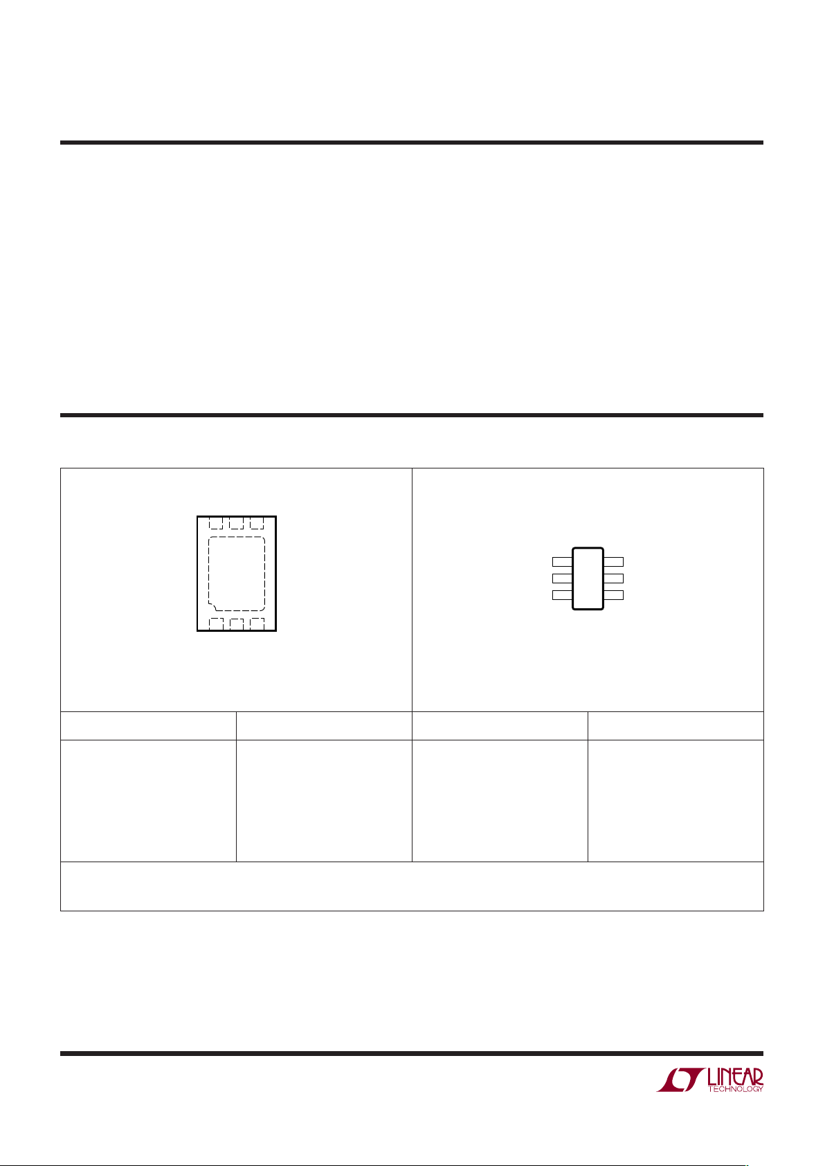
PACKAGE/ORDER I FOR ATIO
UUW
TOP VIEW
MOD
OUT2
OUT1
SET
V
+
GND
DCB PACKAGE
6-LEAD (2mm × 3mm) PLASTIC DFN
4
5
7
6
3
2
1
T
JMAX
= 125°C, θJA = 64°C/W
EXPOSED PAD (PIN 7) IS GND, MUST BE SOLDERED TO PCB
V+ 1
GND 2
SET 3
6 OUT1
5 OUT2
4 MOD
TOP VIEW
S6 PACKAGE
6-LEAD PLASTIC TSOT-23
T
JMAX
= 150°C, θJA = 230°C/W
ORDER PART NUMBER DCB PART MARKING* ORDER PART NUMBER S6 PART MARKING*
LTC6908CDCB-1
LTC6908IDCB-1
LTC6908CDCB-2
LTC6908IDCB-2
LBXZ
LBXZ
LBYB
LBYB
LTC6908CS6-1
LTC6908IS6-1
LTC6908HS6-1
LTC6908CS6-2
LTC6908IS6-2
LTC6908HS6-2
LTBYC
LTBYC
LTBYC
LTBYD
LTBYD
LTBYD
Order Options Tape and Reel: Add #TR
Lead Free: Add #PBF Lead Free Tape and Reel: Add #TRPBF
Lead Free Part Marking: http://www.linear.com/leadfree/
Consult LTC Marketing for parts specifi ed with wider operating temperature ranges. *The temperature grade is identifi ed by a label on the shipping container.
Specifi ed Temperature Range (Note 3)
LTC6908CS6-1/LTC6908CS6-2 ................ 0°C to 70°C
LTC6908IS6-1/LTC6908IS6-2 .............. –40°C to 85°C
LTC6908HS6-1/LTC6908HS6-2 .........–40°C to 125°C
LTC6908CDCB-1/LTC6908CDCB-2 ..........0°C to 70°C
LTC6908IDCB-1/LTC6908IDCB-2 ......... –40°C to 85°C
Storage Temperature Range (S6) ........... –65°C to 150°C
Storage Temperature Range (DCB) ........ –65°C to 125°C
Lead Temperature (Soldering, 10sec) ...................300°C
LTC6908-1/LTC6908-2
3
690812fa
The
●
denotes the specifi cations which apply over the full operating
temperature range, otherwise specifi cations are at T
A
= 25°C. Test conditions are V+ = 2.7V to 5.5V, RL = 5k, CL = 5pF unless otherwise
noted. The modulation is turned off (MOD is connected to OUT2) unless otherwise specifi ed. R
SET
is defi ned as the resistor connected
from the SET pin to the V
+
pin.
ELECTRICAL CHARACTERISTICS
SYMBOL PARAMETER CONDITIONS MIN TYP MAX UNITS
Δf
OUT
Frequency Accuracy (Note 4) V+ = 2.7V 250kHz ≤ f
OUT
≤ 5MHz
250kHz ≤ f
OUT
≤ 5MHz
50kHz ≤ f
OUT
< 250kHz
●
●
±0.5
±2
±2.5
±1.5
±2.5
±3.5
%
%
%
V
+
= 5V 250kHz ≤ f
OUT
≤ 5MHz
250kHz ≤ f
OUT
≤ 5MHz
50kHz ≤ f
OUT
< 250kHz
5MHz < f
OUT
≤ 10MHz
●
●
●
±1
±2.5
±3
±3.5
±2
±3
±4
±4.5
%
%
%
%
R
SET
Frequency Setting Resistor Range V+ = 2.7V | Δf
OUT
| ≤ 1.5%
| Δf
OUT
| ≤ 2.5%
| Δf
OUT
| ≤ 3.5%
●
●
20
20
400
400
400
2000
k
k
k
V
+
= 5V | Δf
OUT
| ≤ 2%
| Δf
OUT
| ≤ 3%
| Δf
OUT
| ≤ 4%
| Δf
OUT
| ≤ 4.5%
●
●
●
20
20
400
10
400
400
2000
20
k
k
k
k
Δf
OUT
/ΔT Frequency Drift Over Temperature R
SET
= 100k
●
±0.004 %/°C
Δf
OUT
/ΔV+Frequency Drift Over Supply (Note 4) V+ = 2.7V to 3.6V, R
SET
= 100k
V
+
= 4.5V to 5.5V, R
SET
= 100k
●
●
0.04
0.4
0.25
0.9
%/V
%/V
Period Variation
(Frequency Spreading)
R
SET
= 100k, MOD Pin = V+, GND or OPEN
●
±7.5 ±10 ±12.5 %
Long-Term Stability of Output
Frequency (Note 8)
300 ppm/√kHr
Duty Cycle (Note 5) No Modulation, 250kHz ≤ f
OUT
≤ 1MHz
●
45 50 55 %
V
+
Operating Supply Range
●
2.7 5.5 V
I
S
Power Supply Current R
SET
= 2000k, RL = ∞, f
OUT
= 50kHz, MOD Pin = V
+
V+ = 5V
V
+
= 2.7V
●
●
0.4
0.4
0.65
0.6
mA
mA
R
SET
= 20k, RL = ∞, f
OUT
= 5MHz, MOD Pin = GND
V
+
= 5V
V
+
= 2.7V
●
●
1.25
0.9
1.7
1.3
mA
mA
V
IH_MOD
High Level MOD Input Voltage
●
V+ – 0.4 V
V
IL_MOD
Low Level MOD Input Voltage
●
0.4 V
I
MOD
MOD Pin Input Current (Note 6) MOD Pin = V+, V+ = 5V
MOD Pin = GND, V
+
= 5V
●
●
–4
2
–2
4µA
µA
V
OH
High Level Output Voltage (Note 6)
(OUT1, OUT2)
V+ = 5V IOH = –0.3mA
I
OH
= –1.2mA
●
●
4.75
4.4
4.9
4.7
V
V
V
+
= 2.7V IOH = –0.3mA
I
OH
= –0.8mA
●
●
2.35
1.85
2.6
2.2
V
V
V
OL
Low Level Output Voltage (Note 6) V+ = 5V IOL = 0.3mA
I
OL
= 1.2mA
●
●
0.05
0.2
0.15
0.5
V
V
V+ = 2.7V IOL = 0.3mA
I
OL
= 0.8mA
●
●
0.1
0.4
0.3
0.7
V
V
t
r
Output Rise Time (Note 7) V+ = 5V
V
+
= 2.7V
6
11
ns
ns
t
f
Output Fall Time (Note 7) V+ = 5V
V
+
= 2.7V
5
9
ns
ns
LTC6908-1/LTC6908-2
4
690812fa
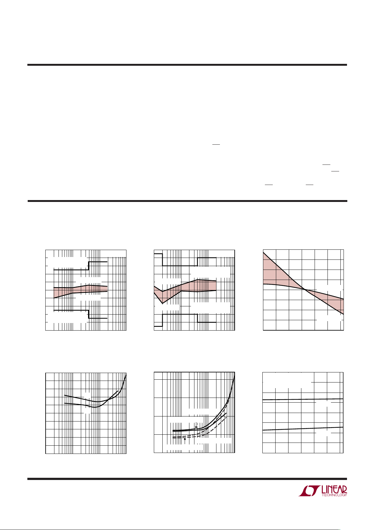
TEMPERATURE (°C)
–
40
SUPPLY CURRENT (µA)
20
60
690812 G06
–
20 0 40
800
4
00
45
0
5
00
55
0
6
00
65
0
7
00
75
0
80
V+ = 5V
V+ = 3V
CL 5pF ON BOTH OUTPUTS
FREQUENCY = 1MHz
SSFM DISABLED
R
SET
(Ω)
10k
FREQUENCY ERROR (%)
5
4
3
2
1
0
–1
–2
–3
–4
–5
100k 1M 10M
690812 G01
TA = 25°C
TYPICAL MAX
GUARANTEED MAX
OVER TEMPERATURE
GUARANTEED MIN
OVER TEMPERATURE
TYPICAL MIN
R
SET
(Ω)
10k
FREQUENCY ERROR (%)
5
4
3
2
1
0
–1
–2
–3
–4
–5
100k 1M 10M
690812 G02
TA = 25°C
TYPICAL MAX
GUARANTEED MAX
OVER TEMPERATURE
GUARANTEED MIN
OVER TEMPERATURE
TYPICAL MIN
TEMPERATURE (°C)
–
40
FREQUENCY ERROR (%)
20
60
690812 G03
–
20 0 40
1.00
0.75
0.50
0.25
0
–
0.25
–
0.50
–
0.75
–
1.00
80
TYPICAL MAX
TYPICAL MIN
FREQUENCY (Hz)
10k
JITTER (%
P-P
)
1.0
0.9
0.8
0.7
0.6
0.5
0.4
0.3
0.2
0.1
0
100k 1M 10M
690812 G04
5V
3V
FREQUENCY (Hz)
10k
SUPPLY CURRENT (mA)
2.0
1.5
1.0
0.5
0
100k 1M 10M
690812 G05
5V SSFM DISABLED
3V SSFM DISABLED
5V SSFM ENABLED
3V SSFM ENABLED
Frequency Error vs R
SET
,
V
+
= 3V
Frequency Error vs R
SET
,
V
+
= 5V Frequency Error vs Temperature
Peak to Peak Jitter vs Output
Frequency
Supply Current vs Output
Frequency Supply Current vs Temperature
TYPICAL PERFOR A CE CHARACTERISTICS
UW
Note 1: Stresses beyond those listed under Absolute Maximum Ratings
may cause permanent damage to the device. Exposure to any Absolute
Maximum Rating condition for extended periods may affect device
reliability and lifetime.
Note 2: LTC6908C and LTC6908I are guaranteed functional over the
operating temperature range of –40°C to 85°C.
Note 3: LTC6908C is guaranteed to meet specifi ed performance from
0°C to 70°C. The LTC6908C is designed, characterized and expected to
meet specifi ed performance from –40°C to 85°C but is not tested or QA
sampled at these temperatures. The LTC6908I is guaranteed to meet
the specifi ed performance limits from –40°C to 85°C. The LTC6908H is
guaranteed to meet the specifi ed performance limits from –40°C to 125°C.
Note 4: Frequency accuracy is defi ned as the deviation from the f
OUT
equation.
Note 5: Guaranteed by 5V test
Note 6: To conform to the Logic IC Standard, current out of a pin is
arbitrarily given a negative value.
Note 7: Output rise and fall times are measured between the 10% and the
90% power supply levels with no output loading. These specifi cations are
based on characterization.
Note 8: Long term drift on silicon oscillators is primarily due to the
movement of ions and impurities within the silicon and is tested at 30°C
under otherwise nominal operating conditions. Long term drift is specifi ed
as ppm/√kHr due to the typically non-linear nature of the drift. To calculate
drift for a set time period, translate that time into thousands of hours, take
the square root and multiply by the typical drift number. For instance, a
year is 8.77kHr and would yield a drift of 888ppm at 300ppm/√kHr. Ten
years is 87.7kHr and would yield a drift of 2,809 ppm at 300 ppm/√kHr.
Drift without power applied to the device may be approximated as 1/10th
of the drift with power, or 30ppm/√kHr for a 300ppm/√kHr device.
ELECTRICAL CHARACTERISTICS
LTC6908-1/LTC6908-2
5
690812fa
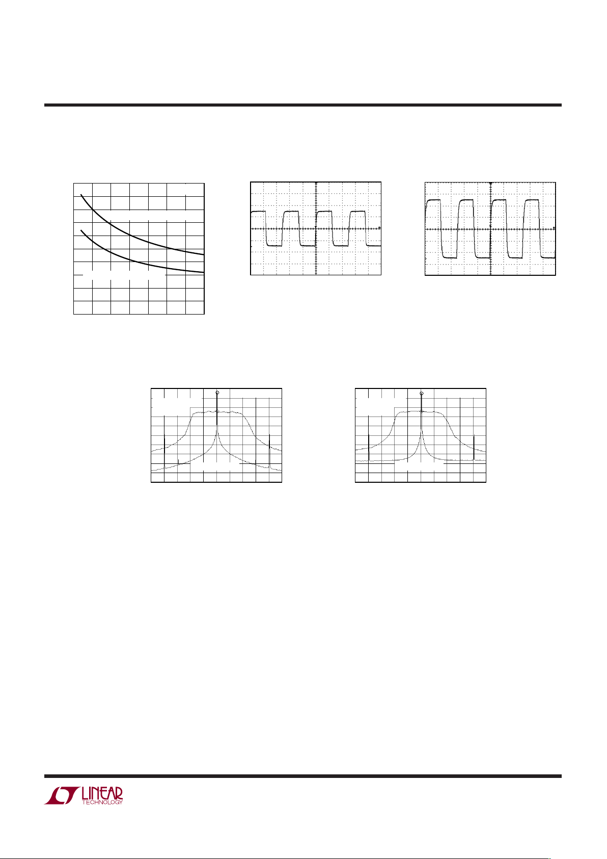
690812 G10
150kHz
FREQUENCY (7.5kHz/DIV)
SSFM DISABLED
RES BW = 220Hz
SSFM ENABLED
(N = 16)
20dBm
–
80dBm
10dB/DIV
690812 G11
5MHz
20dBm
–80dBm
10dB/DIV
FREQUENCY (250kHz/DIV)
SSFM DISABLED
RES BW = 9kHz
SSFM ENABLED
(N = 16)
690812 G09
40ns/DIV
V
OUT
(1V/DIV)
SUPPLY VOLTAGE (V)
2.5
OUTPUT RESISTANCE (Ω)
4.5
5.5
690812 G07
3.0 3.5
4.0 5.0
0
5
0
1
00
15
0
2
00
4
00
45
0
5
00
25
0
3
00
35
0
6.0
OUTPUT SINKING CURRENT
OUTPUT SOURCING CURRENT
TA = 25°C
Output Resistance vs Supply
Voltage
TYPICAL PERFOR A CE CHARACTERISTICS
UW
Output Operating at 5MHz,
V
+
= 3V
Output Operating at 10MHz,
V+ = 5V
Output Frequency Spectrum with
SSFM Enabled and Disabled
Output Frequency Spectrum with
SSFM Enabled and Disabled
690812 G08
80ns/DIV
V
OUT
(1V/DIV)
 Loading...