

FEATURES
■
1kHz to 68MHz Square Wave Output
■
0.5% (Typ) Initial Frequency Accuracy
■
Frequency Error <1.1% Over All Settings
■
10ppm/°C Typical Frequency Drift Over
Temperature
■
0.1% Resolution
■
1.7mA Typical Supply Current (f < 1MHz, VS = 2.7V)
■
2.7V to 5.5V Single Supply Operation
■
Jitter <0.4% Typical 1kHz to 8MHz
■
Easy to Use SPI (LTC6903) or I2C (LTC6904) Serial
Interface
■
Output Enable Pin
■
–40°C to 125°C Operation
■
MS8 Package
U
APPLICATIO S
■
Precision Digitally Controlled Oscillator
■
Power Management
■
Direct Digital Frequency Synthesis (DDS)
Replacement
■
Replacement for DAC and VCO
■
Switched Capacitor Filter Clock
LTC6903/LTC6904
1kHz - 68MHz Serial
Port Programmable Oscillator
U
DESCRIPTIO
The LTC®6903/LTC6904 are low power self contained
digital frequency sources providing a precision frequency
from 1kHz to 68MHz, set through a serial port. The
LTC6903/LTC6904 require
than a power supply bypass capacitor, and they operate
over a single wide supply range of 2.7V to 5.5V.
The LTC6903/LTC6904 feature a proprietary feedback
loop that linearizes the relationship between digital control
setting and frequency, resulting in a very simple frequency
setting equation:
OCT
f
=
2078
⎛
2
⎜
⎝
–
DAC
1024
Where OCT is a 4-bit digital code and DAC is a 10-bit digital
code.
The LTC6903 is controlled by a convenient SPI compatible
serial interface. The LTC6904 uses an industry standard
I2C compatible interface.
, LT, LTC and LTM are registered trademarks of Linear Technology Corporation.
All other trademarks are the property of their respective owners. Protected by U.S. Patents
including 6342817 and 6614313.
no external components
Hz
()
kHz f MHz
<<2
168•
;
⎞
⎟
⎠
other
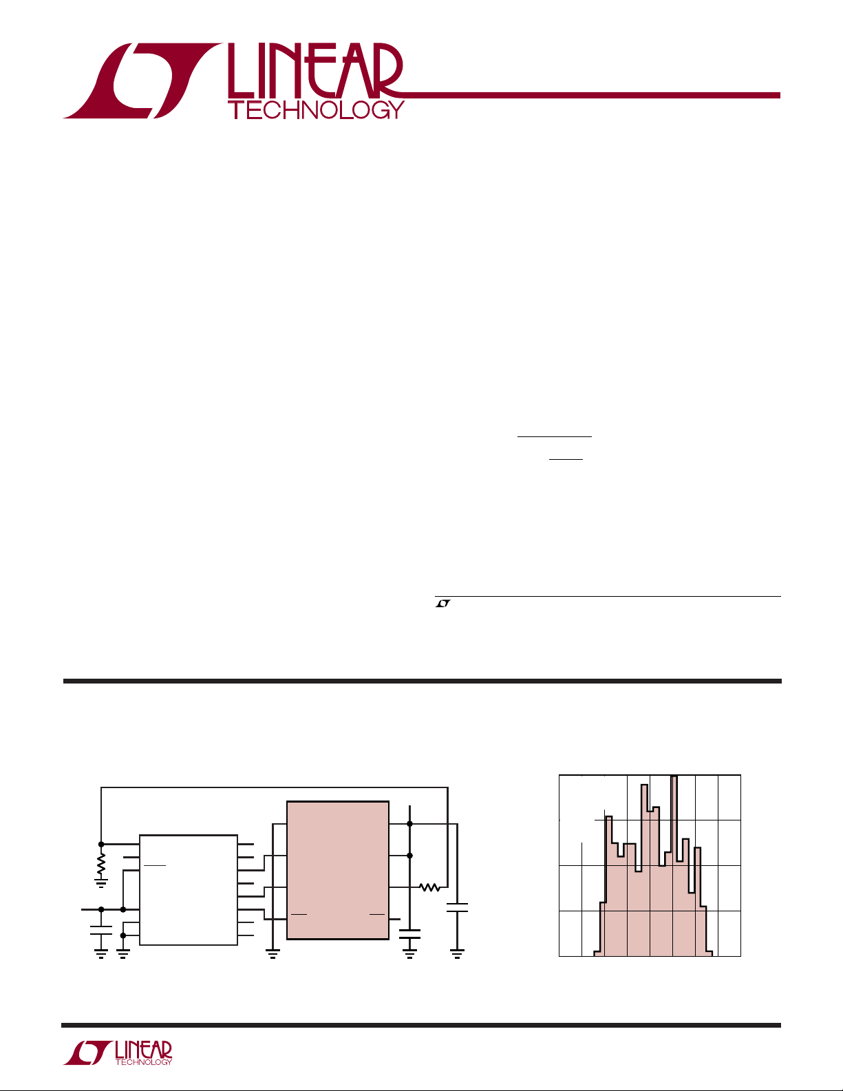
TYPICAL APPLICATIO
A Microcontroller Controlling Its Clock
MICROCONTROLLER
OSC1/CLKIN
10k
5V
0.1μF
OSC2/CLKOUT
MCLR/V
P–P
RC3/SCK/SCL
V
DD
V
SS
V
SS
PIC16F73
RC5/SDO
RC2/CCP1
U
GND
SDI
LTC6903
SCK
SEN
POWER-UP CLOCK
FREQUENCY IS 1039Hz
CLK
CLK
LTC6903 Frequency Error
Distribution
40
VS = 3V
= 25°C
T
30
20
UNITS
10
f = 1039Hz
443
UNITS
TESTED
0
–1.0
A
–0.5
FREQUENCY ERROR (%)
0 0.5 1.0
6903 TA01b
69034fb
5V
+
V
OE
10Ω
1μF
0.01μF
6903 TA01
1
LTC6903/LTC6904
WW
W
ABSOLUTE AXI U RATI GS
U
UUW
PACKAGE/ORDER I FOR ATIO
(Note 1)
Total Supply Voltage (V+ to GND) .............................. 6V
Maximum Voltage on any Pin
........................... (GND – 0.3V) ≤ VPIN ≤ (V+ + 0.3V)
Output Short Circuit Duration (Note 2) ............ Indefinite
Operating Temperature Range (Note 3)
LTC6903CMS8/LTC6904CMS8 ........... –40°C to 85°C
LTC6903IMS8/LTC6904IMS8 ............. –40°C to 85°C
LTC6903HMS8/LTC6904HMS8 ......... –40°C to 125°C
Specified Temperature Range (Note 4)
LTC6903CMS8/LTC6904CMS8 ........... –40°C to 85°C
LTC6903IMS8/LTC6904IMS8 ............. –40°C to 85°C
LTC6903HMS8/LTC6904HMS8 ......... –40°C to 125°C
Storage Temperature Range ..................–65°C to 150°C
Lead Temperature (Soldering, 10sec)................... 300°C
ELECTRICAL CHARACTERISTICS
The ● denotes the specifications which apply over the full operating
TOP VIEW
GND
1
SDI
2
SCK
SEN/ADR*
*SEN (LTC6903)
ADR (LTC6904)
*The temperature grade
Consult LTC Marketing for parts specified with wider operating temperature ranges.
3
4
MS8 PACKAGE
8-LEAD PLASTIC MSOP
T
= 150°C, θJA = 200°C/W
JMAX
+
8
V
7
OE
6
CLK
5
CLK
is identified by a label on the shipping container.
ORDER PART
NUMBER
LTC6903CMS8
LTC6903IMS8
LTC6903HMS8
LTC6904CMS8
LTC6904IMS8
LTC6904HMS8
MS8 PART MARKING*
LTABN
LTAES
temperature range, otherwise specifications are at TA = 25°C. V+ = 2.7V to 5.5V, GND = 0V, unless otherwise noted.
SYMBOL PARAMETER CONDITIONS MIN TYP MAX UNITS
Δfi Initial Frequency Accuracy f = 1.039kHz, V+ = 3V, C
Δf Total Frequency Accuracy (Note 7) Single Output Active:
Over All Settings, V+ = 2.7V, C
Over All Settings, V
LTC6903CMS8, LTC6904CMS8:
Over All Settings, V
Over All Settings, V
LTC6903HMS8, LTC6903IMS8,
LTC6904HMS8, LTC6904IMS8:
Over All Settings, V
Over All Settings, V
f
MAX
f
MIN
Δf/ΔT Frequency Drift Over Temperature 10 ppm/°C
Δf/ΔV Frequency Drift Over Supply 0.05 %/V
R
OUT
V
OH
V
OL
Maximum Operating Frequency 68 MHz
Minimum Operating Frequency 1.039 kHz
Long Term Frequency Stability 300 ppm/√kHr
Timing Jitter 1.039kHz to 8.5MHz 0.4 %
(See Graph) 1.039kHz to 68MHz 1 %
Duty Cycle 1.039kHz to 1MHz ● 49 50 51 %
1.039kHz to 68MHz 50 %
Output Resistance CLK, CLK Pins, V+ = 2.7V 45 Ω
High Level Output Voltage V+ = 5.5V, 4mA Load ● 4.8 5.3 V
Low Level Output Voltage V+ = 5.5V, 4mA Load ● 0.15 0.3 V
+
= 2.7V, 4mA Load ● 2 2.3 V
V
V+ = 5.5V, 1mA Load ● 5.2 5.45 V
+
= 2.7V, 1mA Load ● 2.3 2.55 V
V
+
= 2.7V, 4mA Load ● 0.25 0.45 V
V
V+ = 5.5V, 1mA Load ● 0.05 0.15 V
+
= 2.7V, 1mA Load ● 0.05 0.2 V
V
+
+
+
+
+
= 5pF ±0.75 %
LOAD
= 5pF 0.5 1.1 %
= 5.5V, C
= 2.7V, C
= 5.5V, C
= 2.7V, C
= 5.5V, C
LOAD
= 5pF 0.5 1.6 %
LOAD
= 5pF ● 0.5 1.65 %
LOAD
= 5pF ● 0.5 2 %
LOAD
= 5pF ● 0.5 1.9 %
LOAD
= 5pF ● 0.5 2.2 %
LOAD
69034fb
2
LTC6903/LTC6904
ELECTRICAL CHARACTERISTICS
temperature range, otherwise specifications are at T
SYMBOL PARAMETER CONDITIONS MIN TYP MAX UNITS
t
r
t
f
Output Rise Time (10% - 90%) V+ = 5.5V, R
Output Fall Time (10% - 90%) V+ = 5.5V, R
The ● denotes the specifications which apply over the full operating
= 25°C. V+ = 2.7V to 5.5V, GND = 0V, unless otherwise noted.
A
+
V
= 2.7V, R
+
= 2.7V, R
V
LOAD
LOAD
LOAD
LOAD
= ∞, C
= ∞, C
= ∞, C
= ∞, C
= 5pF 1 ns
LOAD
= 5pF 1 ns
LOAD
= 5pF 1 ns
LOAD
= 5pF 1 ns
LOAD
WU
POWER REQUIRE E TS
range, otherwise specifications are at T
SYMBOL PARAMETER CONDITIONS MIN TYP MAX UNITS
V
S
IS, SHDN V+ Supply Current, Shutdown VS = 2.7V ● 0.25 0.6 mA
IS, DC V+ Supply Current, Single Output f = 68MHz, 5pF Load, V+ = 2.7V ● 3.6 7 mA
Supply Voltage Applied Between V+ and GND ● 2.7 5.5 V
Enabled f < 1MHz, V
= 25°C. V+ = 2.7V to 5.5V, GND = 0V, unless otherwise noted.
A
SERIAL PORT ELECTRICAL CHARACTERISTICS
the full operating temperature range, otherwise specifications are at TA = 25°C. V+ = 2.7V to 5.5V, GND = 0V, unless otherwise noted.
SYMBOL PARAMETER CONDITIONS MIN TYP MAX UNITS
V
IH
V
IL
I
IN
Min High Level Input Voltage ● 0.67 V
SEN, SCK, SDI Pins
Max Low Level Input Voltage ● 0.33 V
SEN, SCK, SDI Pins
Digital Input Leakage ● 10 μA
SEN, SCK, SDI Pins
The ● denotes the specifications which apply over the full operating temperature
= 5.5V ● 0.6 2.2 mA
V
S
+
= 2.7V ● 1.7 3.1 mA
f = 68MHz, 5pF Load, V
f < 1MHz, V
+
= 5.5V ● 1.9 4.5 mA
+
= 5.5V ● 715 mA
The ● denotes the specifications which apply over
+
+
V
V
UW
TI I G CHARACTERISTICS
range, otherwise specifications are at TA = 25°C. V+ = 2.7V to 5.5V, GND = 0V, unless otherwise noted.
SYMBOL PARAMETER MIN TYP MAX UNITS
LTC6903 (Notes 5, 6)
f
SCK
t
CKHI
t
CKLO
t
su
t
hLD
t
LCH
t
FCK
LTC6904 (Notes 5, 6)
f
SMB
t
BUF
t
HD, STA
t
SU, STA
t
SU, STO
Serial Port Clock Frequency ● 20 MHz
Min Clock High Time ● 25 ns
Min Clock Low Time ● 25 ns
Min Setup Time - SDI to SCK ● 10 ns
Min Hold Time - SCK to SDI ● 10 ns
Min Latch Time - SEN to SEN ● 400 ns
Min First Clock - SEN to SCK ● 20 ns
SMBus Operating Frequency ● 10 100 kHz
Bus Free Time Between Stop and Start Condition ● 4.7 μs
Hold Time After (Repeated) Start Condition ● 4.0 μs
Repeated Start Condition Setup Time ● 4.7 μs
Stop Condition Setup Time ● 4.0 μs
The ● denotes specifications which apply over the full operating temperature
69034fb
3
LTC6903/LTC6904
TEMPERATURE (°C)
–40 –20 0 20 40 60 80 120100
FREQUENCY (%)
6903 G03
0.10
0.06
0.02
0.08
0.04
0
–0.02
–0.04
–0.06
–0.08
–0.10
UW
TI I G CHARACTERISTICS
range, otherwise specifications are at T
SYMBOL PARAMETER MIN TYP MAX UNITS
LTC6904 (Notes 5, 6)
t
HD, DAT
t
SU, DAT
t
LOW
t
HIGH
t
f
t
r
Note 1: Stresses beyond those listed under Absolute Maximum Ratings
may cause permanent damage to the device. Exposure to any Absolute
Maximum Rating condition for extended periods may affect device
reliability and lifetime.
Note 2: A heatsink may be required to keep the junction temperature
below the absolute maximum when the output is shorted indefinitely.
Note 3: The LTC6903CMS8, LTC6904CMS8, LTC6903IMS8, and
LTC6904IMS8 are guaranteed functional over the operating temperature
range of –40°C to 85°C. The LTC6903HMS8 and LTC6904HMS8 are
guaranteed functional over the extended operating temperature range of
–40°C to 125°C.
Note 4: The LTC6903CMS8 and LTC6904CMS8 are guaranteed to meet
Data Hold Time ● 300 ns
Data Setup Time ● 250 ns
Clock Low Period ● 4.7 μs
Clock High Period ● 4.0 50 μs
Clock, Data Fall Time ● 300 ns
Clock, Data Rise Time ● 1000 ns
= 25°C. V+ = 2.7V to 5.5V, GND = 0V, unless otherwise noted.
A
The ● denotes specifications which apply over the full operating temperature
the specified performance limits over the 0°C to 70°C temperature range
and are designed, characterized and expected to meet the specified
performance from –40°C to 85°C but are not tested or QA sampled at
these temperatures. The LTC6903IMS8 and LTC6904IMS8 are guaranteed
to meet the specified performance limits over the –40°C to 85°C
temperature range. The LTC6903HMS8 and LTC6904HMS8 are
guaranteed to meet the specified performance limits over the –40°C to
125°C temperature range.
Note 5: All values are referenced to V
Note 6: Guaranteed by design and not subject to test.
Note 7: Parts with tighter frequency accuracy are available. Consult LTC
Marketing for details.
and VIL levels.
IH
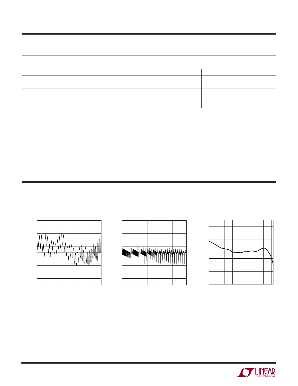
TYPICAL PERFOR A CE CHARACTERISTICS
Integral Nonlinearity
1.0
0.8
0.6
0.4
0.2
0
–0.2
–0.4
–0.6
INTEGRAL NONLINEARITY (LSB)
–0.8
–1.0
0 200 400 600 800 1000
4
DAC SETTING
UW
6903 G01
Differential Nonlinearity
1.0
0.8
0.6
0.4
0.2
0
–0.2
–0.4
–0.6
DIFFERENTIAL NONLINEARITY (LSB)
–0.8
–1.0
0 200 400 600 800 1000
DAC SETTING
Frequency vs Temperature
6903 G01
69034fb

UW
SUPPLY VOLTAGE (V)
3.5 4.52.5 3.0 4.0 5.0 5.5
OUTPUT RESISTANCE (Ω)
6903 G06
60
50
40
30
20
10
0
TYPICAL PERFOR A CE CHARACTERISTICS
LTC6903/LTC6904
Peak-to-Peak Jitter vs Frequency
10
V+ = 3V
1
0.1
PEAK-TO-PEAK JITTER (%)
0.01
0.1 1 10 100
FREQUENCY (MHz)
Output Spectrum at 20MHz
20
0
10dB/DIV
–80
15MHz 25MHz
20MHz
6903 G04
Supply Current vs Output
Frequency
10
9
8
7
6
5
4
3
SUPPLY CURRENT (mA)
2
1
0
0.001 0.01 0.1 1 10 100
FREQUENCY (MHz)
V+ = 5V
V+ = 3V
Output Waveform at 68MHz
0.5V/DIV
CL = 10pF
+
V
= 3V
5ns/DIV
6903 G05
3468 G08
Output Resistance vs Supply
Voltage
Output Waveform at 20MHz
0.5V/DIV
= 10pF
C
L
+
V
= 3V
10ns/DIV
3468 G09
6903 G07
U
UU
PI FU CTIO S
GND (Pin 1): Negative Power Supply (Ground). Should be
tied directly to a ground plane for best performance.
SDI ( Pin 2 ): Serial Data Input. Data for serial transfer is
presented on this pin.
SCK (Pin 3): Serial Port Clock. Input, positive edge triggered. Clocks serial data in on rising edge.
SEN (Pin 4): Serial Port Enable (6903 Only). Input, active
LOW. Initiates serial transaction when brought LOW,
finalizes transaction when brought HIGH after 16 clocks.
ADR (Pin 4): Serial Port Address (6904 Only). Sets the I2C
serial port address.
CLK (Pin 5): Auxiliary Clock Output. Frequency set by
serial port.
CLK (Pin 6): Main Clock Output. Frequency set by serial
port.
OE (Pin 7): Asynchronous Output Enable. CLK and CLK are
set LOW when this pin is LOW.
V+ (Pin 8): Positive Power Supply. This supply must be
kept free from noise and ripple. It should be bypassed
directly to a ground plane with a quality 0.1μF capacitor.
Additional bypass may be necessary for operation at high
frequency or under larger loads.
69034fb
5

LTC6903/LTC6904
OCTf=
⎛
⎝
⎜
⎞
⎠
⎟
3 322
1039
. log
W
BLOCK DIAGRA
+
V
8
OE
CLK CLK
67
5
+
–
+
A1
–
I
SET
DAC OCT
V
SET
fMO = 68MHz • kΩ
GND
21 3 4
SDI SCK SEN (LTC6903)
U
THEORY OF OPERATIO
The LTC6903/LTC6904 contain an internal feedback loop
which controls a high frequency square wave VCO operating between 34MHz and 68MHz. The internal feedback
loop frequency is set over an octave by a 10-bit resistor
DAC. The VCO tracks the internal feedback loop frequency
and the output frequency of the VCO is divided by one of
sixteen possible powers of two.
Higher VCO frequencies and lower output divider settings
can result in higher output jitter. Random jitter at the lower
MASTER
OSCILLATOR
SERIAL PORT
I
SET
V+ – V
ADR (LTC6904)
SET
PROGRAMMABLE
DIVIDER
6903 BD
frequency ranges is very low because of the high output
divisor.
The higher frequency settings will display some deterministic jitter from coupling between the control loop and the
output. This shows up in the frequency spectrum as spurs
separated from the fundamental frequency by 1MHz to
2MHz.
U
WUU
APPLICATIO S I FOR ATIO
Frequency Setting Information
The frequency output of the LTC6903/LTC6904 is determined by the following equation:
Hz
2078
OCT
f
=
2
•
where DAC is the integer value from 0-1023 represented
by the serial port register bits DAC[9:0] and OCT is the
integer value from 0-15 represented by the serial port
register bits OCT [3:0].
6
()
DAC
⎛
2
–
⎜
⎝
1024
⎞
⎟
⎠
Use the following two steps to choose binary numbers
“OCT” and “DAC” in order to set frequency “f”:
1) Use Table 1 to Choose “OCT” or use the following
formula, rounding down to the integer value less than or
equal to the result.
2) Choose “DAC” by the following formula, rounding DAC
to the nearest integer:
DAC
=+2048
–
()•
OCT
10
()
Hz
2078 2
f
69034fb

LTC6903/LTC6904
U
WUU
APPLICATIO S I FOR ATIO
Table 1. Output Frequency Range vs OCT Setting
(Frequency Resolution 0.001 • f)
f ≥ f < OCT
34.05MHz 68.03MHz 15
17.02MHz 34.01MHz 14
8.511MHz 17.01MHz 13
4.256MHz 8.503MHz 12
2.128MHz 4.252MHz 11
1.064MHz 2.126MHz 10
532kHz 1063kHz 9
266kHz 531.4kHz 8
133kHz 265.7kHz 7
66.5kHz 132.9kHz 6
33.25kHz 66.43kHz 5
16.62kHz 33.22kHz 4
8.312kHz 16.61kHz 3
4.156kHz 8.304kHz 2
2.078kHz 4.152kHz 1
1.039kHz 2.076kHz 0
For example, to set a frequency of 6.5MHz, first look at
Table 1 to find an OCT value. 6.5MHz falls between
4.25MHz and 8.5MHz yielding an OCT value of 12 or 1100.
Substituting the OCT value of 12 and the desired frequency
of 6.5MHz into the previous equation results in:
+
10 12
()
Hz
2078 2
DAC
==
2048
–
Rounding 707.113 to the nearest integer yields a DAC
value of 707 (or a 10-bit digital word of 1011000011.)
()•
eHz
65 6
.()
707 113
.
clock frequency. This helps to minimize jitter and subharmonics at the output of the device. In the highest
frequency ranges, the division ratio is reduced, which will
result in greater cycle-to-cycle jitter as well as spurs at the
internal sampling frequency. Because the internal control
loop runs at 1MHz to 2MHz without regard to the output
frequency, output spurs separated from the set frequency
by 1MHz to 2MHz may be observed. These spurs are
characteristically more than 30dB below the level of the set
frequency.
Frequency Settling
When frequency settings change, the settling time and
shape differ depending on which bits are changed. Changing only the OCT bits will result in an instantaneous change
in frequency for OCT values below 10. Values of 10 and
above may take up to 100μs to settle due to the action of
internal power conservation circuitry.
Changing the DAC bits will result in a smooth transition
between the frequencies, occupying at most 100μs, with
little overshoot.
Changing both the OCT and DAC bits simultaneously may
result in considerable excursion beyond the frequencies
requested before settling.
It should be noted that changing the DAC bits at the lower
frequency ranges will result in a seemingly instantaneous
frequency change because the settling time depends on
the internal loop frequency rather than the set frequency.
Power Supply Bypass
Power Up State
When power is first applied to the LTC6903/LTC6904, all
register values are automatically reset to 0. This results in
an output frequency of 1.039kHz with both outputs active.
Output Spectrum
In most frequency ranges, the output of the LTC6903/
LTC6904 is generated as a division of the higher internal
In order to obtain the accuracies represented in this
datasheet, it is necessary to provide excellent bypass on
the power supply. Adequate bypass is a 1μF capacitor in
parallel with a 0.01μF capacitor connected within a few
millimeters of the power supply leads.
Monotonicity and Linearity
The DAC in the LTC6903/LTC6904 is guaranteed to be
10-bit monotonic. Nonlinearity of the DAC is less than 1%.
69034fb
7

LTC6903/LTC6904
U
WUU
APPLICATIO S I FOR ATIO
Additionally, the LTC6903/LTC6904 is guaranteed to be
monotonic when switching between octaves with the OCT
setting bits. For example, the frequency output with a DAC
setting of “1111111111” and an OCT setting of “1100” will
always be lower than the frequency output with a DAC
setting of “0000000000” and an OCT setting of “1101”.
Linearity at these transition points is typically around
3 LSBs.
Output Loading and Accuracy
Improper loading of the outputs of the LTC6903/LTC6904,
especially with poor power supply bypassing, will result in
accuracy problems. At low frequencies, capacitive loading
of the output is not a concern. At frequencies above 1MHz,
attention should be paid to minimize the capacitive load on
the CLK and CLK pins.
The LTC6903/LTC6904 is designed to drive up to 5pF on
each output with no degradation in accuracy. 5pF is
equivalent to one to two HC series logic inputs. A standard
10x oscilloscope probe usually presents between 10pF
and 15pF of capacitive load.
It is strongly suggested that a high speed buffer is used
when driving more than one or two logic inputs, when
driving a line more than 5 centimeters in length, or a
capacitive load greater than 5pF.
Output Control
The CLK and CLK outputs of the LTC6903/LTC6904 are
individually controllable through the serial port as
described in Table 2 below. The low power mode may also
be accessed through these control bits. It is preferred that
unused outputs be disabled in order to reduce power
dissipation and improve accuracy.
Disabling an unused output will improve accuracy of
operation at frequencies above 1MHz. An unused output
running with no load typically degrades frequency accuracy up to 0.2% at 68MHz. An unused output running into
a 5pF load typically degrades frequency accuracy up to
0.5% at 68MHz.
Table 2. Output Configuration
CNF1 CNF0 CLK CLK
0 0 ON CLK + 180°
0 1 OFF ON
1 0 ON OFF
1 1 Powered-Down*
*Powered-Down: When in this mode, the chip is in a low power state and will require approximately 100μs
to recover. This is not the same effect as the OE pin, which is fast, but uses more power supply current.
Serial Port Bitmap (LTC6903/LTC6904)
(All serial port register bits default LOW at power up)
Table 3
D15 D14 D13 D12 D11 D10 D9 D8
OCT3 OCT2 OCT1 OCT0 DAC9 DAC8 DAC7 DAC6
D7 D6 D5 D4 D3 D2 D1 D0
DAC5 DAC4 DAC3 DAC2 DAC1 DAC0 CNF1 CNF0
SEN
SCK
8
SDI
Timing Diagram (LTC6903)
D15 D14 D13 D12 D11 D10 D8D9 D7 D6 D5 D4 D3 D2 D1 D0
6903 TD01
69034fb

LTC6903/LTC6904
U
WUU
APPLICATIO S I FOR ATIO
Serial Port Register Description
OCT[3:0] - Frequency Divider Setting. (See Frequency
Setting Section)
DAC[9:0] - Master Oscillator Frequency Setting. (See
Frequency Setting Section)
CNF[1:0] - Output Configuration - This controls outputs
CLK and CLK according to Table 2.
LTC6903 SPI Compatible Interface
A serial data transfer is composed of sixteen (16) bits of
data labeled D15 through D0. D15 is the first bit of data
presented in each transaction. All serial port register bits
are set LOW on power-up.
WUW
TI I G DIAGRA S
Writing Data (LTC6903 Only)
When the SEN line is brought LOW, serial data presented
on the SDI input is clocked in on the rising edges of SCK
until SEN is brought HIGH. On every eighth rising edge of
SCK, the preceding 8-bits of data are clocked into the
internal register. It is therefore possible to clock in only the
8 {D15 - D8} most significant bits of data rather than
completing an entire transfer.
The serial data transfer starts with the most significant bit
and ends with the least significant bit of the data, as shown
in the timing diagram.
SDA
SCL
SDA
t
SU, DAT
t
HIGH
t
t
r
f
SCL
t
HD, STA
START
CONDITION
t
LOW
Typical LTC6904 Input Waveform—Programming Frequency to 68MHz (ADR Pin Set LOW)
ADDRESS
001011ADRWR
00101110
123
456789123456789123456789
Timing Diagram (LTC6904)
t
HD, DAT
REPEATED START
CONDITION
OCT3 OCT2 OCT1 OCT0 DAC9 DAC8 DAC7 DAC6
11111111
ACK
t
SU, STA
t
HD, STA
t
BUF
t
SU, STO
STOP
CONDITION
DAC5 DAC4 DAC3 DAC2 DAC1 DAC0 CNF1 CNF0
11111100
ACK
START
CONDITION
6903 TD02
STOPSTART
ACK
6903 TD03
69034fb
9

LTC6903/LTC6904
TYPICAL APPLICATIO S
U
LTC6904 I2C Interface
The LTC6904 communicates with a host (master) using
2
the standard I
C 2-wire interface. The Timing Diagram
shows the timing relationship of the signals on the bus.
The two bus lines, SDA and SCL, must be high when the
bus is not in use. External pull-up resistors or current
sources, such as the LTC1694 SMBus Accelerator, are
required on these lines. If the I
2
with a standard I
C compatible device, care must be taken
2
C interface is not driven
to ensure that the SDA line is released during the ACK
cycle to prevent bus contention.
The LTC6904 is a receive-only (slave) device. The master
can communicate with the LTC6904 using the Write Word
protocols as explained later.
The START and STOP Conditions
When the bus is not in use, both SCL and SDA must be
high. A bus master signals the beginning of a communication to a slave device by transmitting a START condition. A START condition is generated by transitioning SDA
from high to low while SCL is high.
When the master has finished communicating with the
slave, it issues a STOP condition. A STOP condition is
generated by transitioning SDA from low to high while
SCL is high. The bus is then free for communication with
another SMBus device.
Acknowledge
The Acknowledge signal is used for handshaking between
the master and the slave. An Acknowledge (active LOW)
generated by the slave lets the master know that the latest
byte of information was received. The Acknowledge related clock pulse is generated by the master. The master
releases the SDA line (HIGH) during the Acknowledge
clock pulse. The slave-receiver must pull down the SDA
line during the Acknowledge clock pulse so that it remains
a stable LOW during the HIGH period of this clock pulse.
Write Word Protocol
The master initiates communication with the LTC6904
with a START condition and a 7-bit address followed by the
Write Bit (Wr) = 0. The LTC6904 acknowledges and the
master delivers the most significant data byte. Again the
LTC6904 acknowledges and the data is latched into the
most significant data byte input register. The master then
delivers the least significant data byte. The LTC6904
acknowledges once more and latches the data into the
least significant data byte input register. Lastly, the master
terminates the communication with a STOP condition.
Slave Address
The LTC6904 can respond to one of two 7-bit addresses.
The first 6 bits (MSBs) have been factory programmed to
001011. The address pin, ADR (Pin 4) is programmed by
the user and determines the LSB of the slave address, as
shown in the table below:
ADR (Pin 4) LTC6904 Address
0 0010111
1 0010110
10
Write Word Protocol Used by the LTC6904
711818
Slave Address AWr MS Data Byte A LS Data Byte A PS
S = Start Condition, Wr = Write Bit = 0, A = Acknowledge, P = Stop Condition
111
6903 AI01
69034fb

PACKAGE DESCRIPTIO
U
MS8 Package
8-Lead Plastic MSOP
(Reference LTC DWG # 05-08-1660)
0.889 ± 0.127
(.035 ± .005)
LTC6903/LTC6904
5.23
(.206)
MIN
0.42 ± 0.038
(.0165 ± .0015)
TYP
RECOMMENDED SOLDER PAD LAYOUT
0.254
(.010)
GAUGE PLANE
0.18
(.007)
NOTE:
1. DIMENSIONS IN MILLIMETER/(INCH)
2. DRAWING NOT TO SCALE
3. DIMENSION DOES NOT INCLUDE MOLD FLASH, PROTRUSIONS OR GATE BURRS.
MOLD FLASH, PROTRUSIONS OR GATE BURRS SHALL NOT EXCEED 0.152mm (.006") PER SIDE
4. DIMENSION DOES NOT INCLUDE INTERLEAD FLASH OR PROTRUSIONS.
INTERLEAD FLASH OR PROTRUSIONS SHALL NOT EXCEED 0.152mm (.006") PER SIDE
5. LEAD COPLANARITY (BOTTOM OF LEADS AFTER FORMING) SHALL BE 0.102mm (.004") MAX
DETAIL “A”
(.126 – .136)
(.0256)
° – 6° TYP
0
DETAIL “A”
3.20 – 3.45
0.65
BSC
0.53 ± 0.152
(.021 ± .006)
SEATING
PLANE
3.00 ± 0.102
(.118 ± .004)
(NOTE 3)
4.90
± 0.152
(.193 ± .006)
(.043)
0.22 – 0.38
(.009 – .015)
TYP
1.10
MAX
8
12
0.65
(.0256)
BSC
7
0.52
5
4
(.0205)
REF
3.00 ± 0.102
(.118 ± .004)
(NOTE 4)
0.86
(.034)
REF
0.1016 ± 0.0508
(.004 ± .002)
MSOP (MS8) 0307 REV F
6
3
Information furnished by Linear Technology Corporation is believed to be accurate and reliable.
However, no responsibility is assumed for its use. Linear Technology Corporation makes no representation that the interconnection of its circuits as described herein will not infringe on existing patent rights.
69034fb
11

LTC6903/LTC6904
TYPICAL APPLICATIO
Wide Range Time Interval Generator (1.97 Seconds to 4 Microseconds)
1
< TRIGGER PULSE WIDTH < OUTPUT PULSE WIDTH
f
CLK
TRIG
1
GND
SDI
SCK
SEN
S0
S1
S2
2
SDI
3
SCK
4
SEN
MUX SELECT ADDRESS LINES
U6
LTC6903
CLK
CLK
+
V
8
+
V
7
OE
6
5
C2
0.1μF
f
CLK
U
+
V
4
D
+
V
16
CLK
11
MR
52
U4
63
QQRPSCLK
1
74HC74-A
PHILIPS SEMICONDUCTOR
C1
0.1μF
910
Q1
7
Q2
6
Q3
5
Q4
3
Q5
2
Q6
4
Q7
13
Q8
12
Q9
14
Q10
15
Q11
1
Q12
8
74HC4040
PHILIPS
SEMICONDUCTOR
+
V
C3
0.1μF
16
4
D0
3
D1
2
D2
1
D3
15
D4
14
D5
13
D6
12
D7
11
S0
10
S1
9
S2
7
OE
Y
Y
U1
8
74HC251
PHILIPS
SEMICONDUCTOR
6
5
Q
OUT
10
D
U5
CLK
13
+
V
74HC74-B
PHILIPS
SEMICONDUCTOR
QRPS
Q
912
811
6903 TA02
OUTPUT
PULSE
WIDTH
n
2
=
f
CLK
V
OUT
V
OUT
MUX Inputs
Output
S2 S1 S0 n Pulsewidth
000416/f
100532/f
010664/f
1107128/f
0018256/f
1019512/f
0 1 1 10 1024/f
1 1 1 11 2048/f
CLK
CLK
CLK
CLK
CLK
CLK
CLK
CLK
RELATED PARTS
PART NUMBER DESCRIPTION COMMENTS
LTC1799 1kHz to 30MHz ThinSOT™ Oscillator Single Output, Higher Frequency Operation
LTC6900 1kHz to 20MHz ThinSOT Oscillator Single Output, Lower Power
LTC6902 Multiphase Oscillator with Spread Spectrum Modulation 2, 3 or 4-Phase Outputs
ThinSOT is a trademark of Linear Technology Corporation
LT 0807 REV B • PRINTED IN USA
12
Linear Technology Corporation
1630 McCarthy Blvd., Milpitas, CA 95035-7417
(408) 432-1900 ● FAX: (408) 434-0507 ● www.linear.com
© LINEAR TECHNOLOGY CORPORATION 2003
69034fb
 Loading...