

FEATURES
■
One External Resistor Sets the Frequency
■
1kHz to 20MHz Frequency Range
■
500µA Typical Supply Current, VS = 3V, 3MHz
■
Frequency Error ≤1.5% Max, 5kHz to 10MHz
(TA = 25°C)
■
Frequency Error ≤2% Max, 5kHz to 10MHz
(TA = 0°C to 70°C)
■
±40ppm/°C Temperature Stability
■
0.04%/V Supply Stability
■
50% ±1% Duty Cycle 1kHz to 2MHz
■
50% ±5% Duty Cycle 2MHz to 10MHz
■
Fast Start-Up Time: 50µs to 1.5ms
■
100Ω CMOS Output Driver
■
Operates from a Single 2.7V to 5.5V Supply
■
Low Profile (1mm) ThinSOTTM Package
U
APPLICATIO S
■
Portable and Battery-Powered Equipment
■
PDAs
■
Cell Phones
■
Low Cost Precision Oscillator
■
Charge Pump Driver
■
Switching Power Supply Clock Reference
■
Clocking Switched Capacitor Filters
■
Fixed Crystal Oscillator Replacement
■
Ceramic Oscillator Replacement
LTC6900
Low Power, 1kHz to 20MHz
Resistor Set SOT-23 Oscillator
U
DESCRIPTIO
The LTC®6900 is a precision, low power oscillator that is
easy to use and occupies very little PC board space. The
oscillator frequency is programmed by a single external
resistor (R
accuracy operation (≤1.5% frequency error) without the
need for external trim components.
The LTC6900 operates with a single 2.7V to 5.5V power
supply and provides a rail-to-rail, 50% duty cycle square
wave output. The CMOS output driver ensures fast rise/fall
times and rail-to-rail switching. The frequency-setting
resistor can vary from 10kΩ to 2MΩ to select a master
oscillator frequency between 100kHz and 20MHz (5V
supply). The three-state DIV input determines whether the
master clock is divided by 1, 10 or 100 before driving the
output, providing three frequency ranges spanning 1kHz
to 20MHz (5V supply). The LTC6900 features a proprietary
feedback loop that linearizes the relationship between
R
and frequency, eliminating the need for tables to
SET
calculate frequency. The oscillator can be easily programmed using the simple formula outlined below:
f MHz
=•
OSC
, LTC and LT are registered trademarks of Linear Technology Corporation.
ThinSOT is a trademark of Linear Technology Corporation.
). The LTC6900 has been designed for high
SET
100
,
DIV Pin V
N Open
=
,
10
,
DIV Pin
1
,
DIV Pin GND
10
NR
•
20
k
SET
=
=
=
+
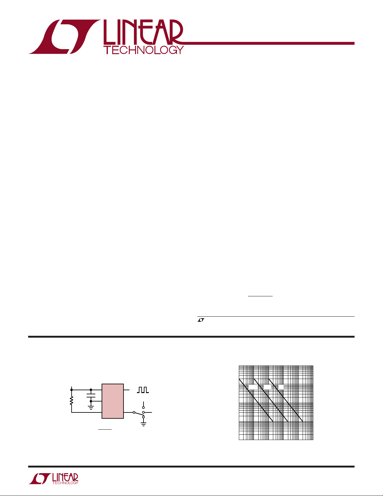
TYPICAL APPLICATIO
Clock Generator
10k ≤ R
SET
≤ 2M
5V
f
OSC
0.1µF
= 10MHz •
1
+
OUT
V
LTC6900
2
GND
3
SET
DIV
20k
()
N • R
SET
U
1kHz ≤ f
5
4
OSC
5V, N = 100
N = 1
≤ 20MHz
OPEN, N = 10
6900 TA01
R
vs Desired Output Frequency
SET
10000
1000
(kΩ)
SET
R
100
÷100 ÷10 ÷1
10
1
1k 100k 1M 10M
10k
DESIRED OUTPUT FREQUENCY (Hz)
100M
6900 F02
6900f
1
LTC6900
TOP VIEW
S5 PACKAGE
5-LEAD PLASTIC SOT-23
1
2
3
V
+
GND
SET
54OUT
DIV
PACKAGE/ORDER I FOR ATIO
UU
W
WWWU
ABSOLUTE AXI U RATI GS
(Note 1)
Supply Voltage (V+) to GND ........................– 0.3V to 6V
DIV to GND ....................................–0.3V to (V+ + 0.3V)
SET to GND ...................................–0.3V to (V+ + 0.3V)
Operating Temperature Range (Note 8)
LTC6900C .......................................... – 40°C to 85°C
LTC6900I............................................ –40°C to 85°C
Storage Temperature Range ................. –65°C to 150°C
Lead Temperature (Soldering, 10 sec).................. 300°C
ORDER PART NUMBER
LTC6900CS5
LTC6900IS5
S5 PART MARKING
T
= 150°C, θJA = 256°C/W
JMAX
Consult LTC Marketing for parts specified with wider operating temperature ranges.
LTZM
ELECTRICAL CHARACTERISTICS
The ● denotes the specifications which apply over the full operating
temperature range, otherwise specifications are at TA = 25°C. V+ = 2.7V to 5.5V, RL= 5k, CL = 5pF, Pin 4 = V+ unless otherwise noted.
All voltages are with respect to GND.
SYMBOL PARAMETER CONDITIONS MIN TYP MAX UNITS
∆f Frequency Accuracy (Notes 2, 3) V+ = 5V 5kHz ≤ f ≤ 10MHz ±0.5 ±1.5 %
V+ = 3V 5kHz ≤ f ≤ 10MHz ±0.5 ±1.5 %
R
SET
∆f/∆T Freq Drift Over Temp (Note 3) R
∆f/∆V Freq Drift Over Supply (Note 3) V+ = 3V to 5V, R
+
V
I
S
V
IH
V
IL
I
DIV
Frequency-Setting Resistor Range ∆f < 1.5% V+ = 5V 20 400 kΩ
= 63.2k ● ±0.004 %/°C
SET
Timing Jitter (Note 4) Pin 4 = V+, 20k ≤ R
Pin 4 = Open, 20k ≤ R
Pin 4 = 0V, 20k ≤ R
Long-Term Stability of Output Frequency 300 ppm/√kHr
Duty Cycle (Note 7) Pin 4 = V+ or Open (DIV Either by 100 or 10) ● 49 50 51 %
Pin 4 = 0V (DIV by 1), R
Operating Supply Range ● 2.7 5.5 V
Power Supply Current R
High Level DIV Input Voltage ● V+ – 0.4 V
Low Level DIV Input Voltage ● 0.5 V
DIV Input Current (Note 5) Pin 4 = V
= 400k, Pin 4 = V+, RL = ∞ V+ = 5V ● 0.32 0.42 mA
SET
f
= 5kHz V+ = 3V ● 0.29 0.38 mA
OSC
R
= 20k, Pin 4 = 0V, RL = ∞ V+ = 5V ● 0.92 1.20 mA
SET
= 10MHz V+ = 3V ● 0.68 0.86 mA
f
OSC
+
Pin 4 = 0V V
5kHz ≤ f ≤ 10MHz, LTC6900C
5kHz ≤ f ≤ 10MHz, LTC6900I
1kHz ≤ f < 5kHz ±2%
10MHz < f ≤ 20MHz ±2%
5kHz ≤ f ≤ 10MHz, LTC6900C
5kHz ≤ f ≤ 10MHz, LTC6900I
1kHz ≤ f < 5kHz ±2%
+
V
= 63.2k ● 0.04 0.1 %/V
SET
≤ 400k 0.1 %
SET
≤ 400k 0.2 %
SET
≤ 400k 0.6 %
SET
= 20k to 400k ● 45 50 55 %
SET
V+ = 5V ● 2 4 µA
+
● ±2.0 %
● ±2.5 %
● ±2.0 %
● ±2.5 %
= 3V 20 400 kΩ
= 5V ● –4 –2 µA
2
6900f
LTC6900
ELECTRICAL CHARACTERISTICS
The ● denotes the specifications which apply over the full operating
temperature range, otherwise specifications are at TA = 25°C. V+ = 2.7V to 5.5V, RL= 5k, CL = 5pF, Pin 4 = V+ unless otherwise noted.
All voltages are with respect to GND.
SYMBOL PARAMETER CONDITIONS MIN TYP MAX UNITS
V
OH
V
OL
t
r
t
f
Note 1: Absolute Maximum Ratings are those values beyond which the life
of the device may be impaired.
Note 2: Frequencies near 100kHz and 1MHz may be generated using two
different values of R
paragraph in the Applications Information section). For these frequencies,
the error is specified under the following assumption: 20k < R
Note 3: Frequency accuracy is defined as the deviation from the
f
OSC
Note 4: Jitter is the ratio of the peak-to-peak distribution of the period to
the mean of the period. This specification is based on characterization and
is not 100% tested. Also, see the Peak-to-Peak Jitter vs Output Frequency
curve in the Typical Performance Characteristics section.
Note 5: To conform with the Logic IC Standard convention, current out of
a pin is arbitrarily given as a negative value.
High Level Output Voltage (Note 5) V+ = 5V IOH = –1mA ● 4.8 4.95 V
= –4mA ● 4.5 4.8 V
I
OH
V+ = 3V IOH = –1mA ● 2.7 2.9 V
I
= –4mA ● 2.2 2.6 V
OH
Low Level Output Voltage (Note 5) V+ = 5V IOL = 1mA ● 0.05 0.15 V
= 4mA ● 0.2 0.4 V
I
OL
V+ = 3V IOL = 1mA ● 0.1 0.3 V
= 4mA ● 0.4 0.7 V
I
OL
OUT Rise Time V+ = 5V Pin 4 = V+ or Floating, RL = ∞ 14 ns
(Note 6) Pin 4 = 0V, R
V+ = 3V Pin 4 = V+ or Floating, RL = ∞ 19 ns
Pin 4 = 0V, R
OUT Fall Time V+ = 5V Pin 4 = V+ or Floating, RL = ∞ 13 ns
(Note 6) Pin 4 = 0V, R
V+ = 3V Pin 4 = V+ or Floating, RL = ∞ 19 ns
Pin 4 = 0V, R
(see the Selecting the Divider Setting Resistor
SET
≤ 200k.
SET
equation.
= ∞ 7ns
L
= ∞ 11 ns
L
= ∞ 6ns
L
= ∞ 10 ns
L
Note 6: Output rise and fall times are measured between the 10% and
90% power supply levels. These specifications are based on
characterization.
Note 7: Guaranteed by 5V test.
Note 8: The LTC6900C is guaranteed to meet specified performance from
0°C to 70°C. The LTC6900C is designed, characterized and expected to
meet specified performance from –40°C to 85°C but is not tested or QA
sampled at these temperatures. The LTC6900I is guaranteed to meet
specified performance from –40°C to 85°C.
6900f
3
LTC6900
UW
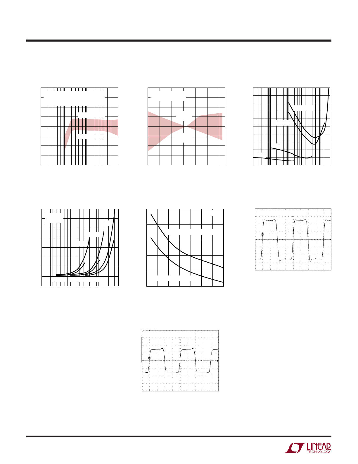
TYPICAL PERFOR A CE CHARACTERISTICS
Frequency Variation vs R
4
TA = 25°C
3
GUARANTEED LIMITS APPLY OVER
20kΩ ≤ R
2
1
0
–1
VARIATION (%)
–2
–3
–4
1k
≤ 400kΩ
SET
10k 100k 1M
R
Supply Current vs Output
Frequency
2.0
TA = 25°C
C
= 5pF
L
1.5
1.0
SUPPLY CURRENT (mA)
0.5
÷100, 3V ÷10, 3V ÷1, 3V
0
0
1k 10k 100k 1M 10M
÷100, 5V
OUTPUT FREQUENCY (Hz)
TYPICAL HIGH
TYPICAL LOW
(Ω)
SET
SET
÷10, 5V
÷1, 5V
6900 G01
6900 G04
Frequency Variation Over
Temperature
1.00
R
= 63.4k
SET
0.75
÷1 OR ÷10 OR ÷100
0.50
0.25
0
–0.25
VARIATION (%)
–0.50
–0.75
–1.00
–20 0 20 40 60 80
–40
TEMPERATURE (°C)
Output Resistance
vs Supply Voltage
140
120
OUTPUT SOURCING CURRENT
100
80
OUTPUT RESISTANCE (Ω)
60
OUTPUT SINKING CURRENT
40
2.5 3.0
3.5
SUPPLY VOLTAGE (V)
TYPICAL
HIGH
TYPICAL
LOW
4.0
4.5
5.0
T
A
6900 G02
= 25°C
5.5
6900 G05
6.0
Peak-to-Peak Jitter vs Output
Frequency
1.0
0.9
0.8
0.7
)
0.6
P-P
0.5
0.4
JITTER (%
0.3
0.2
0.1
0
1k
÷1, VA = 3V
÷10
÷100
OUTPUT FREQUENCY (Hz)
÷1, VA = 5V
100k 1M10k 10M
LTC6900 Output Operating at
20MHz, VS = 5V
V+ = 5V, R
1V/DIV
0V
= 10k, CL = 10pF
SET
12.5ns/DIV
6900 G03
6900 G06
4
LTC6900 Output Operating at
10MHz, VS = 3V
V+ = 3V, R
1V/DIV
0V
= 20k, CL = 10pF
SET
25ns/DIV
6900 G07
6900f
 Loading...