

LTC6702
Tiny Micropower,
Low Voltage
Dual Comparators
FEATURES
n
Low Supply Operation: 1.7V Minimum
n
Low Supply Current: 30μA/Comparator Maximum
n
Propagation Delay: 500ns Maximum (–40°C to
125°C)
n
3.2MHz Toggle Frequency
n
Input Voltage Range Extends 100mV Below Ground
n
Internal Hysteresis: 4mV
n
High Output Drive: TTL and CMOS Compatible
Specifi ed at ±15mA (–40°C to 125°C),
Capacitive Load Handling to 10,000pF
n
Specifi ed for –40°C to 125°C Temperature Range
n
Available in SOT-23 and 2mm × 2mm DFN Package
APPLICATIONS
n
Battery Powered Systems
n
Window Comparators
n
Threshold Detectors/Discriminators
n
Clock Regeneration
n
Automotive Sensing and Controls
DESCRIPTION
The LTC®6702 is an extremely small dual comparator
designed to maximize battery life while providing both
speed and low voltage operation in applications where
board space is a premium.
These comparators operate on supplies between 1.7V and
5.5V, and have a maximum guaranteed propagation delay
of 500ns while drawing only 30μA maximum quiescent
current. Internal hysteresis desensitizes the LTC6702 to
input noise and makes it easy to use, even with slow moving signals. CMOS inputs allow the use of large source
impedances.
The LTC6702 is available in the 8-pin SOT-23 and the tiny
2mm × 2mm DFN package.
L, LT, LTC and LTM are registered trademarks of Linear Technology Corporation.
All other trademarks are the property of their respective owners.
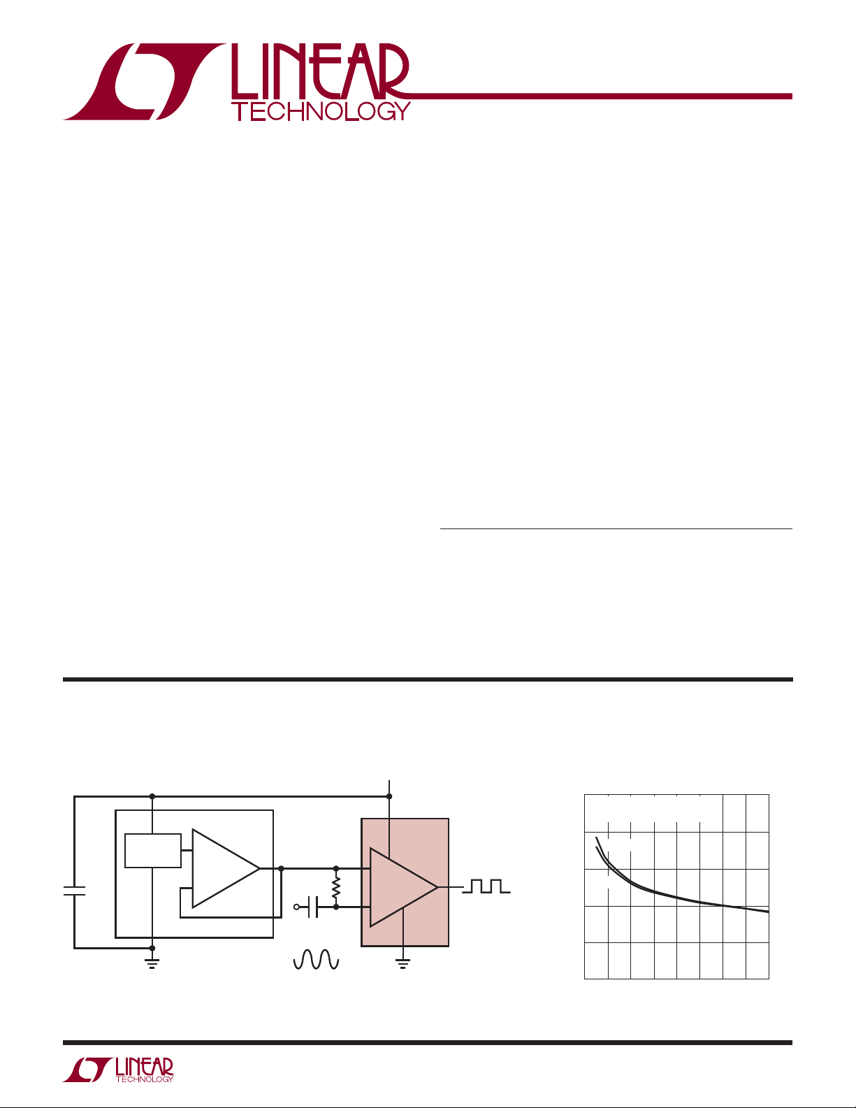
TYPICAL APPLICATION
Clock Regeneration Circuit
LT6650
OUT
FB
CLOCK INPUT > 100mV
0.1MF
IN
VR= 400mV
REFERENCE
+
–
C1
0.1MF
+
= 3V
V
600
V+ = 5V
= 100mV
V
1/2 LTC6702
–
1k
+
P-P
RECOVERED
CLOCK
(UP TO 3.2MHz)
6702 TA01
STEP
500
FALLING
400
RISING
300
PROPAGATION DELAY (ns)
200
100
0
10 20
C
= 10pF
LOAD
= 25°C
T
A
40
30 50 80
INPUT OVERDRIVE (mV)
60 70
6702 TA01b
6702f
1
Propagation Delay vs Input Overdrive
LTC6702
ABSOLUTE MAXIMUM RATINGS
(Note 1)
Supply Voltage (V+ to GND) ........................................6V
Input Voltage ...............................................................6V
Input Current ........................................................–10mA
Output Short-Circuit Duration (Note 2) ............ Indefi nite
Operating Temperature Range (Note 3)
LTC6702C ...........................................–40°C to 85°C
LTC6702I .............................................–40°C to 85°C
LTC6702H .........................................–40°C to 125°C
Specifi ed Temperature Range (Note 4)
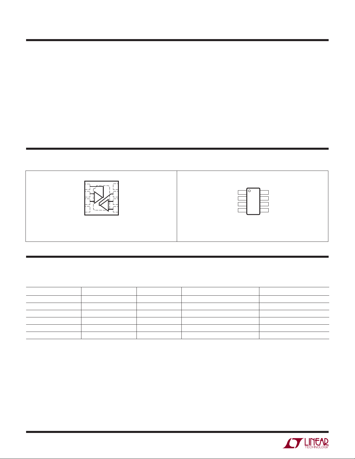
PIN CONFIGURATION
TOP VIEW
+
1
OUT A
2
–IN A
+IN A
GND
8-LEAD (2mm × 2mm) PLASTIC DFN
T
EXPOSED PAD (PIN 9) IS GND, MUST BE SOLDERED TO PCB
A
3
4
DC PACKAGE
= 150°C, θJA = 102°C/W
JMAX
8
9
V
OUT B
7
–IN B
6
B
+IN B
5
LTC6702C ............................................... 0°C to 70°C
LTC6702I .............................................–40°C to 85°C
LTC6702H .........................................–40°C to 125°C
Junction Temperature .......................................... 150°C
Storage Temperature Range ...................–65°C to 150°C
Lead Temperature (Soldering, 10 sec)
TSOT Packages ................................................. 300°C
TOP VIEW
OUT A
–IN A
+IN A
GND
TS8 PACKAGE
8-LEAD PLASTIC TSOT-23
T
= 150°C, θJA = 130°C/W
JMAX
+
V
OUT B
–IN B
+IN B
ORDER INFORMATION
Lead Free Finish
TAPE AND REEL (MINI) TAPE AND REEL PART MARKING* PACKAGE DESCRIPTION TEMPERATURE RANGE
LTC6702CDC#TRMPBF LTC6702CDC#TRPBF LCZJ 8-Lead (2mm × 2mm) Plastic DFN 0°C to 70°C
LTC6702IDC#TRMPBF LTC6702IDC#TRPBF LCZJ 8-Lead (2mm × 2mm) Plastic DFN –40°C to 85°C
LTC6702HDC#TRMPBF LTC6702HDC#TRPBF LCZJ 8-Lead (2mm × 2mm) Plastic DFN –40°C to 125°C
LTC6702CTS8#TRMPBF LTC6702CTS8#TRPBF LTCZK 8-Lead Plastic TSOT-23 0°C to 70°C
LTC6702ITS8#TRMPBF LTC6702ITS8#TRPBF LTCZK 8-Lead Plastic TSOT-23 –40°C to 85°C
LTC6702HTS8#TRMPBF LTC6702HTS8#TRPBF LTCZK 8-Lead Plastic TSOT-23 –40°C to 125°C
TRM = 500 pieces. *Temperature grades are identifi ed by a label on the shipping container.
Consult LTC Marketing for parts specifi ed with wider operating temperature ranges.
Consult LTC Marketing for information on lead based fi nish parts.
For more information on lead free part marking, go to: http://www.linear.com/leadfree/
For more information on tape and reel specifi cations, go to: http://www.linear.com/tapeandreel/
6702f
2
LTC6702
ELECTRICAL CHARACTERISTICS
The l denotes the specifi cations which apply over the full specifi ed
temperature range, otherwise specifi cations are at T
= 25°C. V+ = 3V, VCM = 1.5V, C
A
SYMBOL PARAMETER CONDITIONS MIN TYP MAX UNITS
+
V
I+ Supply Current per Comparator V
Supply Voltage Guaranteed by PSRR
+
= 3V
V+ = 5V
V
OS
Input Offset Voltage (Note 5)
LTC6702C/LTC6702I
LTC6702H
V
HYST
Input Hysteresis Voltage (Note 5)
LTC6702C/LTC6702I
LTC6702H
ΔV
/ΔT Input Offset Voltage Drift (Note 5)
OS
I
IN
Input Leakage Current
LTC6702C/LTC6702I
LTC6702H
CMRR Common Mode Rejection Ratio V
= –0.1V to VDD – 1.2V
CM
Input Voltage Range Guaranteed by CMRR
+
PSRR Power Supply Rejection Ratio V
V
OL
V
OH
t
PD
Δt
t
SKEW
t
r
t
f
f
MAX
I
SC
PD
Output Swing Low Overdrive = 20mV (Note 6)
Output Swing High Overdrive = 20mV (Note 6)
Propagation Delay (Note 7)
Differential Propagation Delay Between Channels 4 ns
Propagation Delay Skew Between t
Output Rise Time 11 ns
Output Fall Time 15 ns
Maximum Toggle Frequency 3.2 MHz
Short-Circuit Current V+ = 5V ±250 mA
= 1.7V to 5.5V, VCM = 0.5V
I
= 100μA
SINK
I
= 15mA
SINK
I
= 100μA
SOURCE
I
= 15mA
SOURCE
PDLH/tPDHL
= 20pF, unless otherwise noted.
OUT
l
1.7 5.5 V
l
l
l
l
2.5
l
1.6
l
1.6
l
4.3 6.2
0.001
l
l
58
l
56
l
–0.1 VDD – 1.2 V
56
l
54
l
l
l
l
320 450
l
24 30
40
25 32
42
1 3.5
5
6
μA
μA
μA
μA
mV
mV
mV
mV
7.2
8.2
6
μV/
mV
mV
°C
nA
1
10
nA
nA
70 dB
dB
65 dB
dB
mV
10
250
mV
mV
mV
10
350
mV
mV
ns
500
ns
4 ns
Note 1: Stresses beyond those listed under Absolute Maximum Ratings
may cause permanent damage to the device. Exposure to any Absolute
Maximum Rating condition for extended periods may affect device
reliability and lifetime.
Note 2: A heat sink may be required to keep the junction temperature
below absolute maximum. This depends on the power supply voltage and
how many comparators are shorted. The θ
specifi ed for the DC and
JA
TS packages is with minimal PCB heat spreading metal. Using expanded
metal area on all layers of a board reduces this value.
Note 3: The LTC6702C and LTC6702I are guaranteed functional over
the temperature range of –40°C to 85°C. The LTC6702H is guaranteed
functional over the operating temperature range of –40°C to 125°C.
Note 4: The LTC6702C is guaranteed to meet specifi ed performance from
0°C to 70°C. The LTC6702C is designed, characterized and expected to
meet specifi ed performance from –40°C to 85°C but is not tested or
QA sampled at these temperatures. The LTC6702I is guaranteed to meet
specifi ed performance from –40°C to 85°C. The LTC6702H is guaranteed
to meet specifi ed performance from –40°C to 125°C.
Note 5: The LTC6702 comparators include internal hysteresis. The offset
voltage is defi ned as the average of the input voltages (trip points)
required to change the output in each direction minus V
, while the
CM
hysteresis voltage is the difference of these trip points.
Note 6: Output voltage swings are measured between the output and
power supply rails.
Note 7: Propagation delay is for 200mV steps, and 50mV of overdrive.
Overdrive is measured relative to the positive and negative trip points.
6702f
3
LTC6702
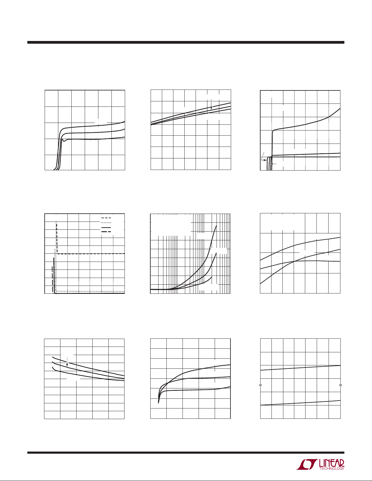
TYPICAL PERFORMANCE CHARACTERISTICS
Supply Current
vs Supply Voltage
50
40
30
20
10
SUPPLY CURRENT PER COMPARATOR (μA)
0
0
234
1
SUPPLY VOLTAGE (V)
Input Offset Current
vs Input Voltage
100
V+ = 3V
90
80
70
60
50
40
30
20
INPUT OFFSET CURRENT (pA)
10
0
–1
0
2
1
INPUT VOLTAGE (V)
125°C
25°C
–55°C
56
6702 G01
Supply Current
vs Temperature
35
30
25
20
15
10
5
SUPPLY CURRENT PER COMPARATOR (μA)
0
–50
–25 0
V+ = 5V
V+ = 1.7V
50 100 125
25 75
TEMPERATURE (°C)
V+ = 3V
6702 G02
Input Leakage Current
vs Input Voltage
5
V+ = 3V
4
3
2
1
–55°C
INPUT LEAKAGE CURRENT (nA)
0
–1
–1
125°C
25°C
1
0
INPUT VOLTAGE (V)
85°C
2
3
4
5
6702 G03
6
Maximum Toggle Rate
Supply Current vs Toggle Rate
450
V
125°C
85°C
25°C
–55°C
3
4
5
6702 G04
400
350
300
250
200
150
100
SUPPLY CURRENT PER COMPARATOR (μA)
6
= 200mV
STEP
OVERDRIVE = 100mV
= 25°C
T
A
NO C
LOAD
50
0
10k
V+ = 5V
V+ = 3V
V+ = 1.7V
100k 1M 10M
TOGGLE RATE (Hz)
6702 G05
vs Temperature
4
V
= 200mV
STEP
OVERDRIVE = 100mV
= 10pF
C
LOAD
3
MAXIMUM TOGGLE RATE (MHz)
2
–50
–25 0
25 75
TEMPERATURE (°C)
V+ = 3V
V+ = 5V
V+ = 1.7V
50 100 125
6702 G06
Input Offset Voltage
vs Supply Voltage Hysteresis vs Supply Voltage
5
4
3
2
1
0
–1
–2
–3
INPUT OFFSET VOLTAGE (mV)
–4
–5
1
25°C
–55°C
2
3
SUPPLY VOLTAGE (V)
4
125°C
5
6
6702 G07
8
7
6
5
4
3
HYSTERESIS (mV)
2
1
0
1
23 5
SUPPLY VOLTAGE (V)
4
Input Common Mode Limits
vs Temperature
+
V
+
–0.5
V
125°C
25°C
–55°C
4
6702 G08
V+–1.0
+
V
–1.5
GND
–0.5
INPUT COMMON MODE LIMITS (V)
6
–1.0
–50
–25 0
50 100 125
25 75
TEMPERATURE (°C)
6702 G09
6702f

TYPICAL PERFORMANCE CHARACTERISTICS
LTC6702
Propagation Delay
vs Supply Voltage
420
400
380
360
340
320
PROPAGATION DELAY (ns)
300
280
V
= 100mV
STEP
= 10pF
C
LOAD
23 5
1
SUPPLY VOLTAGE (V)
Output Low Voltage
vs Load Current
1.0
TA = 25°C
0.1
0.01
OUTPUT VOLTAGE (V)
0.001
0.1
1 10 100
SINK CURRENT (mA)
RISING
FALLING
V+ = 3V
4
V+ = 1.7V
V+ = 5V
25°C, 125°
–55°
RISING
C
FALLING
6702 G10
6702 G13
800
700
600
500
400
PROPAGATION DELAY (ns)
300
6
200
1.0
) (V)
OUT
0.1
-V
+
0.01
OUTPUT VOLTAGE (V
0.001
Propagation Delay
vs Load Capacitance
V
= 100mV
STEP
OVERDRIVE = 50mV
= 25°C
T
A
V+ = 1.7V
FALLING
RISING
V+ = 3V, 5V
10
LOAD CAPACITANCE (pF)
FALLING
100 1000 10000
RISING
6702 011
Output Rise and Fall
Times vs Load Capacitance
1000
V
= 100mV
STEP
OVERDRIVE = 50mV
= 25°C
T
A
100
TIME (ns)
t
f
t
r
t
f
t
r
10
t
f
t
r
1
10
100 1000 10000
LOAD CAPACITANCE (pF)
V+ = 1.7V
+
V
+
V
Output High Voltage
vs Load Current Output Voltage vs Temperature
TA = 25°C
0.1
V+ = 1.7V
V+ = 3V
V+ = 5V
1 10 100
SOURCE CURRENT (mA)
6702 G14
90
HIGH = V+ – V
I
= ±4mA
80
OUT
70
60
V+ = 1.7V
50
40
30
OUTPUT VOLTAGE (mV)
20
V+ = 5V
10
0
–50
0
–25
TEMPERATURE (°C)
OUT
HIGH
LOW
HIGH
LOW
25 125
50
75 100
= 3V
= 5V
6702 G12
6702 G15
V
OUT
1V/DIV
GND
V
50mV/DIV
Propagation Delay Propagation Delay with Load 1MHz Sinusoid Response
10k
V
OUT
1V/DIV
GND
V
50mV/DIV
IN
V+= 3V
= 20pF
C
L
V
CM
200ns/DIV
= 500mV
IN
V+= 3V
= 20pF
C
L
V
CM
= 500mV
100ns/DIV
6702 G16
V
OUT
1V/DIV
GND
V
50mV/DIV
IN
V+= 3V
= 20pF
C
L
100ns/DIV
V
= 500mV
CM
= 10k, 200Ω
R
L
200Ω
6702 G17
6702 G18
6702f
5

LTC6702
PIN FUNCTIONS
OUT A (Pin 1): Output of Comparator A.
–IN A (Pin 2): Inverting Input of Comparator A.
+IN A (Pin 3): Noninverting Input of Comparator A.
GND (Pin 4): Ground.
+IN B (Pin 5): Noninverting Input of Comparator B.
SIMPLIFIED SCHEMATIC
+IN
750
Ω
–IN B (Pin 6): Inverting Input of Comparator B.
OUT B (Pin 7): Output of Comparator B.
+
(Pin 8): Positive Supply Voltage
V
Exposed Pad (Pin 9, DC Package Only): Ground. The
Exposed Pad must be soldered to PCB.
+
V
–IN
750Ω
OUT
GND
6702 SS
6702f
6

APPLICATIONS INFORMATION
LTC6702
The LTC6702 device is a fast (500ns delay), low power,
low voltage (1.7V to 5.5V supply) general purpose dual
comparator. It provides rail-to-rail outputs able to interface
to TTL/CMOS, draws low supply currents (30μA/comparator), and has internal hysteresis (approximately 4mV).
Hysteresis
Each comparator has built-in hysteresis to simplify designs,
to insure stable operation in the presence of noise at the
inputs, and to reject supply rail noise. The reference voltage
applied to the input is not the exact switching threshold
value due to the built-in hysteresis. Actual output switching
typically occurs within ±2.2mV of the reference voltage,
plus or minus the input offset voltage. External positive
feedback circuitry can be employed to increase effective
hysteresis if desired as shown in Figure 1. This circuitry
will provide an apparent effect on both the rising and falling input thresholds (the actual internal trip points remain
unaffected). If an inverting confi guration with hysteresis is
needed, simply swap the V
and V
IN
connections.
REF
Input Protection
External input protection circuitry is only needed if currents
would otherwise exceed the absolute maximum rating.
Inputs driven further negative than 100mV below ground
will not cause damage provided the current is limited to
10mA. ESD protection diodes are provided to prevent
damage during handling.
Comparator Input
The allowable input voltage ranges from 100mV below GND
to within 1.2V of the positive supply. The input may be
forced below ground without causing an improper output,
though some additional input current will begin to fl ow
from the ESD input protection diode. The inputs can reach
+
up to 6V independent of the V
supply voltage without
causing additional input current or damage to the part.
As long as one input is within the allowable input voltage
range, the LTC6702 will continue to function normally.
Comparator Output
Unused Inputs
Any unused inputs should be connected in a way that fi xes
the output logic state high or low. One easy way to do this
+
is to tie +IN to V
R1
V
IN
and –IN to GND.
R3
V
R2
REF
+
1/2 LTC6702
–
6702 F01
The comparator output is a push-pull CMOS stage
+
guaranteed to swing to within 350mV of V
and 250mV
of ground, over temperature when sourcing or sinking
15mA. No external pull-up/down resistor is required. To
R1
Additional Hystersis =
Trip Voltages:
= V
V
IN(LH)
V
IN(HL)
Example: Additional Hysteresis = 50mV, V+= 5V
R1= 10k
R2 = 249k
R3= 1M
FOR V
REF
•R1•
REF
= V
•R1•
REF
= 0.5V: VIN(L H) = 0.525V
V
IN
+
•V
R3
1
1
R2
1
R
1
+
R3
1
+
2
3
R
+
R1
1
+
1
R
(H L) = 0.475V
R1
R
+
•V
3
Figure 1. Additional Hysteresis Circuit for Noninverting Confi guration
6702f
7

LTC6702
APPLICATIONS INFORMATION
maintain micropower operation, the output stage uses a
break-before-make circuit. The break interval of this circuit
turns off both the pull-up and pull-down devices for tens
of nanoseconds before activating the appropriate output
transistor (depends on the output transition direction).
Any load connected to the output will charge or discharge
internal capacitance during this interval. This can create a
soft corner during output transitions and also decrease the
propagation delay. The Typical Per formance Characteristics
section shows this behavior under three load conditions:
unloaded, 10k to ground and 200Ω to ground. Loads to
+
have a similar affect when the output is transitioning
V
from low to high.
Power Supplies
The comparator circuitry operates from a single 1.7V
to 5.5V. A 0.1μF minimum bypass capacitor is required
+
between the V
pin and GND. When the output is sinking
at least 1mA, a 1μF bypass capacitor is recommended.
Pulsing the V+ supply to the comparators on and off may
+
engage the ESD protection circuitry at the V
+
occurs, current is pulled from the V
pin through the output
pin. If this
stage. Using the recommended supply bypass capacitors
+
with some series resistance in the V
supply line will help
to prevent this action in pulsed supply applications.
Level Translators
The level translators in the Typical Applications section
show an adjustable high-precision voltage reference
enabling the user to vary the threshold voltage. Simply
adjusting the ratio of the two resistors changes the threshold voltage according to the following equation:
V
THR
= 0.4 1+
R
F
R
G
TYPICAL APPLICATIONS
LT6650
IN
GND
Low to High Level Translator
500mV
OUT
24.9k
FB
100k
5.5V
–
1/2 LTC6702
1μF0.1μF
2V
0V
+
OUT
5.5V
0V
6702 TA02
8
6702f

TYPICAL APPLICATIONS
LTC6702
High to Low Level Translator
1.8V
C1
0.1μF
R1
909k
R2
332k
R3
1M
IN
0.1μF
LT6650
GND
OUT
500mV
24.9k
FB
100k
1μF0.1μF
6V
0V
Micropower Battery Monitor with Fast Response
LTC6702
LT1790-1.25
OUTIN
GND
1μF
–
1/2 LTC6702
+
V
BATT
+
COMPB
–
–
COMPA
+
6702 TA04
OUT
OUTB (0V IF V
OUTA (0V IF V
1.8V
0V
6702 TA03
BATT
BATT
< 2.1V)
< 2.8V)
6702f
9

LTC6702
PACKAGE DESCRIPTION
DC Package
8-Lead Plastic DFN (2mm × 2mm)
(Reference LTC DWG # 05-08-1719 Rev Ø)
0.70 ±0.05
2.55 ±0.05
1.15 ±0.05
0.64 ±0.05
(2 SIDES)
1.37 ±0.05
(2 SIDES)
RECOMMENDED SOLDER PAD PITCH AND DIMENSIONS
APPLY SOLDER MASK TO AREAS THAT ARE NOT SOLDERED
PIN 1 BAR
TOP MARK
(SEE NOTE 6)
0.200 REF
NOTE:
1. DRAWING IS NOT A JEDEC PACKAGE OUTLINE
2. DRAWING NOT TO SCALE
3. ALL DIMENSIONS ARE IN MILLIMETERS
4. DIMENSIONS OF EXPOSED PAD ON BOTTOM OF PACKAGE DO NOT INCLUDE
MOLD FLASH. MOLD FLASH, IF PRESENT, SHALL NOT EXCEED 0.15mm ON ANY SIDE
5. EXPOSED PAD SHALL BE SOLDER PLATED
6. SHADED AREA IS ONLY A REFERENCE FOR PIN 1 LOCATION ON THE
TOP AND BOTTOM OF PACKAGE
PACKAGE
OUTLINE
0.25 ± 0.05
0.45 BSC
R = 0.05
2.00 ±0.10
(4 SIDES)
0.75 ±0.05
0.00 – 0.05
R = 0.115
TYP
TYP
0.64 ± 0.10
(2 SIDES)
4
BOTTOM VIEW—EXPOSED PAD
1.37 ±0.10
(2 SIDES)
85
1
0.45 BSC
0.40 ± 0.10
PIN 1 NOTCH
R = 0.20 OR
0.25 × 45°
CHAMFER
(DC8) DFN 0106 REVØ
0.23 ± 0.05
10
6702f

PACKAGE DESCRIPTION
LTC6702
TS8 Package
8-Lead Plastic TSOT-23
(Reference LTC DWG # 05-08-1637)
0.52
MAX
3.85 MAX
2.62 REF
RECOMMENDED SOLDER PAD LAYOUT
PER IPC CALCULATOR
0.20 BSC
DATUM ‘A’
0.30 – 0.50 REF
NOTE:
1. DIMENSIONS ARE IN MILLIMETERS
2. DRAWING NOT TO SCALE
3. DIMENSIONS ARE INCLUSIVE OF PLATING
4. DIMENSIONS ARE EXCLUSIVE OF MOLD FLASH AND METAL BURR
5. MOLD FLASH SHALL NOT EXCEED 0.254mm
6. JEDEC PACKAGE REFERENCE IS MO-193
0.65
REF
1.22 REF
1.4 MIN
2.80 BSC
0.09 – 0.20
(NOTE 3)
1.50 – 1.75
(NOTE 4)
1.00 MAX
0.65 BSC
0.80 – 0.90
2.90 BSC
(NOTE 4)
PIN ONE ID
1.95 BSC
0.22 – 0.36
8 PLCS (NOTE 3)
0.01 – 0.10
TS8 TSOT-23 0802
Information furnished by Linear Technology Corporation is believed to be accurate and reliable.
However, no responsibility is assumed for its use. Linear Technology Corporation makes no representation that the interconnection of its circuits as described herein will not infringe on existing patent rights.
6702f
11

LTC6702
TYPICAL APPLICATION
Dual Low Side Current Sense Alarm
5.5V
LED B
1k
LED A
1k
LOAD B
I
LOADB
R
SB
0.17
LT6650
GND
LTC6702
+
V
–
FB
OUTIN
500mV
1MF0.1MF
24.9k
37.4k
COMP B
+
+
LOAD A
I
LOADA
LEDA ON IF I
LEDB ON IF I
LOADA
LOADB
R
SA
0.17
> 2.5A
> 5.0A
61.9k
COMP A
–
GND
6702 TA05
RELATED PARTS
PART NUMBER DESCRIPTION COMMENTS
LTC1441/LTC1442 Dual Ultralow Power Comparators with
Reference
LTC1541/LTC1542 Micropower Amplifi er with Comparator and
Reference
LTC1842/LTC1843 Dual Ultralow Power Comparators with
Reference
LT6660 Tiny Micropower Precision Series References 0.2% Reference, 20ppm/°C Drift, 20mA Output, 2mm × 2mm DFN Package
LT6700-1/LT6700-2/
Dual Comparators with 400mV Reference 1.4V to 18V Operating Range, 18μs Propagation Delay, SOT-23 Package
LT6700-3
LT6703-2/LT6703-3 Tiny Single Comparator with 400mV Reference 1.4V to 18V Operating Range, 18μs Propagation Delay, 2mm × 2mm
1.182V ±1% Reference, 8μs Propagation Delay, 5.7μA
1.2V ±0.8% Reference, Amplifi er Stable with 1000pF Load
1.182V ±1% Reference, 4μs, 3.5μA, Open-Drain Out
DFN Package
12
Linear Technology Corporation
1630 McCarthy Blvd., Milpitas, CA 95035-7417
(408) 432-1900 ● FAX: (408) 434-0507
●
www.linear.com
6702f
LT 0907 • PRINTED IN USA
© LINEAR TECHNOLOGY CORPORATION 2007
 Loading...