Precision, Matched, Baseband Filter ICs Outperform Discrete
Implementations – Design Note 476
Philip Karantzalis
Introduction
In digital communication systems, baseband signals must
be band-limited in the transmitter or the receiver. Although
the bulk of baseband signal shaping and analysis is accomplished using digital signal processing (DSP), analog
fi ltering is used in a number of places along the signal
chain. For instance analog fi lters reduce the imaging of a
digital-to-analog converter (DAC), fi lter out the high frequency noise of an RF demodulator or reduce the aliasing
inputs of an analog-to-digital converter (ADC).
Typically, 3G communication systems (CDMA, GSM,
UMTS or WiMax) feature a baseband channel bandwidth
of 1.25MHz to over 20MHz. In this frequency range, discrete analog fi lters—those constructed with high speed
op amps, resistors and capacitors—are sensitive to PCB
layout parasitics, component tolerances and mismatches.
The pitfalls of using discrete components can be avoided
by using integrated, pin-confi gurable, precision analog
fi lter ICs, such as the LTC6601-1/-2 and the LTC6605-7/
-10/-14. The LTC6601-x is a single 2nd order lowpass fi lter
and the LTC6605-x is a dual, matched fi lter.
The LTC6601-x Lowpass Filter
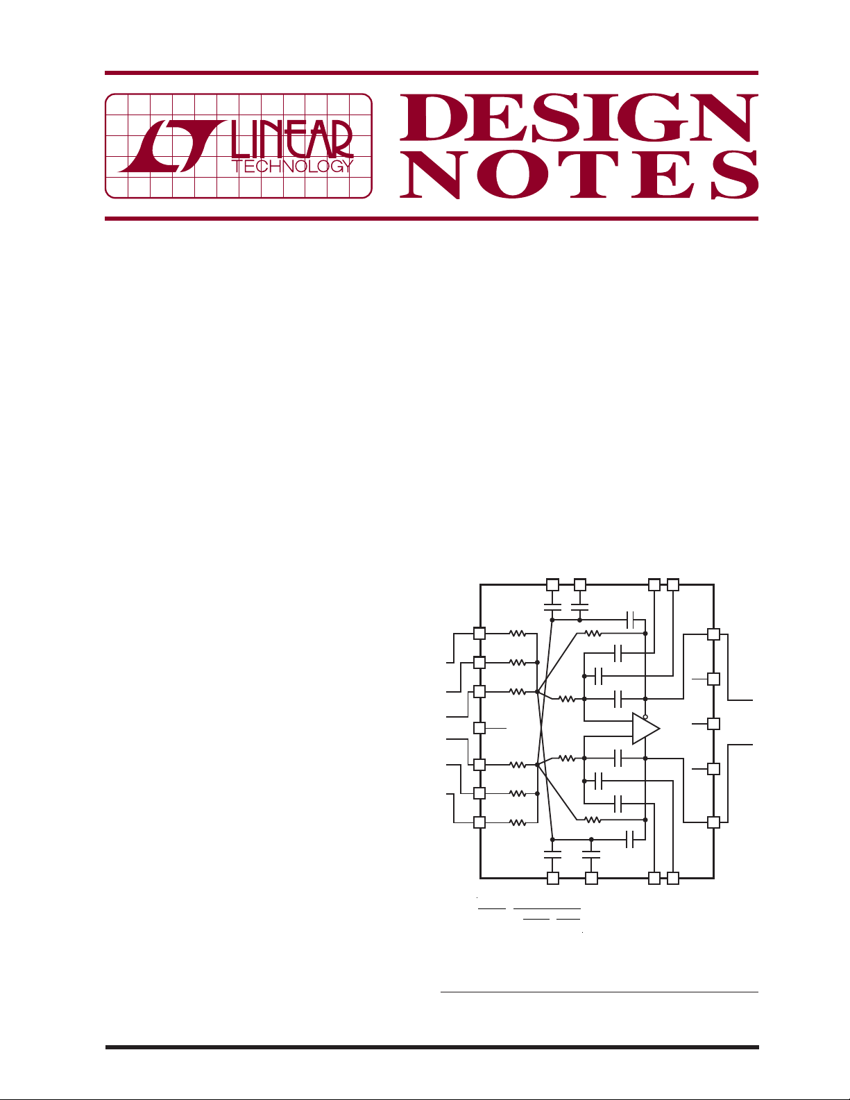
Figure 1 shows a block diagram of an LTC6601-x and the
2nd order function it implements. High frequency fi lters
are easily implemented using the LTC6601-x, which integrates a low noise (1.5nV√Hz) wideband (600MHz), fully
differential amplifi er with precision resistors and capacitors. The standard deviation of the on-chip resistors and
capacitors is ±0.25% and their matching is ±0.1% (in a
differential amplifi er, the common mode rejection at high
frequencies depends on tigh t matching of the signal paths).
Furthermore, the gain bandwidth (GBW) of the LTC6601-x
amplifi er is trimmed to ±5%. Note that this level of precision cannot be achieved with discrete analog fi lters in any
practical manufacturing process.
In many LTC6601-x fi lter implementations, no external
components are required. For instance, lowpass fi lters
can be produced by simply hardwiring the input pins for
a variety of fi lter gain and cutoff frequencies from 5MHz
to 27MHz.
The product and ratio of the on-chip resistors and capacitors determine the f
function. The f
and Q values of the 2nd order fi lter
0
and Q pair sets the fi lter’s cutoff frequency
0
and passband gain peak. The value of the feedback resistor determines the range of the f
frequencies. The 400Ω
0
feedback resistors can be shunted by input resistors to
increase the f
range.
0
Using an LTC6601-x with input RC or LC fi lters, 3rd, 4th and
5th order lowpass fi lters can be implemented (refer to the
LTC6601-1 or -2 data sheet s for higher order fi lter options).
18
19
C6
V
INDIFF
20
1
2
3
4
5
6
V
IN4
IN2
IN1
BIAS
IN1
IN2
IN4
OUTDIFF
V
INDIFF
C5 C717C8
16.1pF
+
400Ω
+
200Ω
+
100Ω
–
100Ω
–
200Ω
–
400Ω
=
1+
16.1pF
2π f
s
O
GAIN
•Q
C1
7
+
(2π fO)
125Ω
125Ω
2
s
2
33.3pF
400Ω
21.1pF
21.1pF
400Ω
81.5pF
10.55pF
48.2pF
48.2pF
10.55pF
81.5pF
33.3pF
C2
Figure 1. Block Diagram of the LTC6601-x and the 2nd Order
Transfer Function it Implements.
L, LT, LTC, LTM, Linear Technology, the Linear logo are registered trademarks of
Linear Technology Corporation. All other trademarks are the property of their respective
owners.
16
–
OUT
15
+
V
14
–
+
V
V
13
OUTDIFF
–
V
OCM
12
+
OUT
11
C3
9C4108
03/10/DN476

The LTC6601 family is offered in two options that trade off
distortion and noise. Use the LTC6601-1 for low noise and
the LTC6601-2 for low distortion at low power.
The LTC6605-x, Dual, Matched, Lowpass Filter
Typically, quadrature down conversion is used in a direct
conversion or zero -IF receiver. In a quadrature demodulator,
the RF signal is split into two paths and mixed with the LO
(local oscillator) to produce an I (in phase) and a Q (90°
phase or quadra ture) signal. In a direct c onversion receiver,
high image rejection depends on very tight gain and phase
matching. High image rejection maximizes the signal-tonoise ratio (SNR) and minimizes the bit error rate.
The LTC6605-x contains two LTC6601 ICs confi gured and
tested as a dual, matched, 2nd order, lowpass fi lter. There
are three LTC6605 versions: the LTC6605-7 with an adjustable f
with an adjustable f
and the LTC6605-14 with an adjustable f
12.4MHz to 20MHz (the f
range of 6.5MHz to 10MHz, the LTC6605-10
(–3dB)
range of 9.7MHz to 14MHz
(–3dB)
(–3dB)
(–3dB)
or f
frequency is set
(–1dB)
range of
by an external resistor).
The maximum gain and phase matching error of an
LTC6605-x is ±0.35dB and ±1.2° respectively (equivalent
to –32dB of image rejection). This level of gain and phase
matching of an LTC6605-x IC is impractical using discrete
resistors and capacitors.
The LTC6605-7 or -10 input pins can be har d wired for gains
of 1, 4 or 5; the LTC6605-14 for gains of 1, 2 or 3. Either
3.3V
10Ω
10Ω
10Ω
10Ω
3.3V
LTC2205
16-BIT ADC
3V
LTC2205
16-BIT ADC
64MHz
I
IN
Q
IN
LTC6605-7
1
+
2
4
–
5
7
+
8
10
–
11
GAIN = 12dB
= 7MHz
f
–1dB
= 9MHz
f
–3dB
49.9Ω
22
I
OUT
49.9Ω
18
49.9Ω
16
Q
OUT
49.9Ω
12
10pF
10pF
10pF
10pF
10pF
10pF
Figure 2. An LTC6605-7 Driving Two LTC2205 ADCs
can produce nonint eger gains using external input r esistors
with a slight reduction in gain and phase matching.
Accurate gain and phase matching, when combined with
very low noise and distortion, allows for a high dynamic
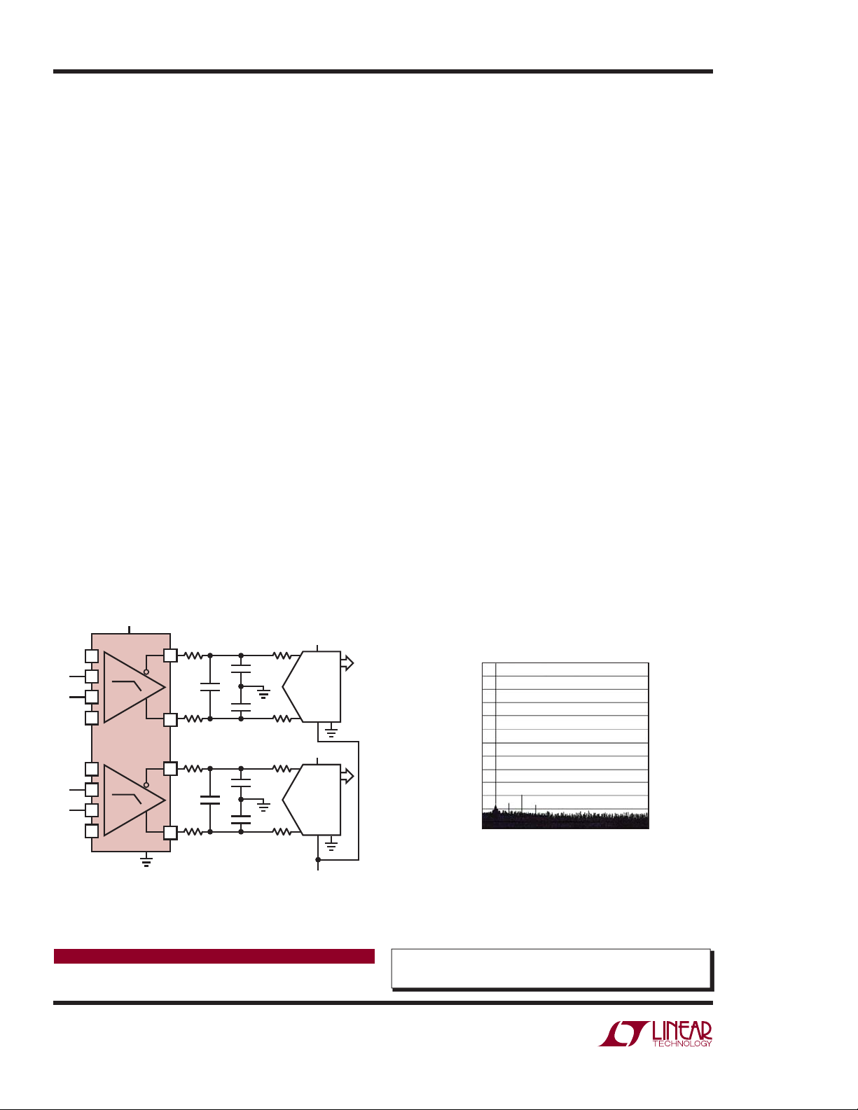
range differential circuit. Figure 2 shows an LTC6605-7
driving a dual LTC2205 16-bit ADC and Figure 3 shows the
FFT plot of the ADC output. The LTC6605-7 is confi gured
for a 12dB gain and a 7MHz, –1dB frequency (suitable
application for WiMax).
As with an LTC6601-x, an LTC6605-x can be used with
input RC or LC fi lters, to implement 3rd, 4th and 5th order
lowpass fi lters. The LTC6605-7 is available in a compact
6mm × 3mm, 22-pin leadless DFN package.
The power consumption for an LTC6601-x and for each
LTC6605-x 2nd order section, is set by a three-state BIAS
pin, allowing a choice between shutdown (I
medium power (I
= 16mA) or full power (IS = 33mA).
S
= 350μA),
S
Conclusion
The LTC6601-x fully differential, lowpass fi lter with precision on-chip resistors and capacitors can be confi gured
by hardwiring pins to implement 2nd order fi lters in a
frequency range of 5MHz to 27MHz.
The LTC6601-x is insensitive to PCB parasitics and is a
higher performance circuit than a discrete analog fi lter.
The LTC6605-x is a dual, matched, 2nd order lowpass fi lter
for driving dual ADCs in a high performance direct conversion receiver. Using RC or LC fi lters with an LTC6601-x or
LTC6605-x, 3rd, 4th or 5th order lowpass fi lters can be
implemented.
0
–10
–20
–30
–40
–50
–60
–70
–80
AMPLITUDE (dBFS)
–90
–100
–110
–120
0
10
5
FREQUENCY (MHz)
15
Figure 3. The FFT Plot of the LTC2205’s I or Q Output
Channels of Figure 2 (75dB SNR, –98dB SFDR, 64K-Point
FFT, 64Msps, fIN = 2.5MHz, –1dBFS).
25
20 30
Data Sheet Download
www.linear.com
Linear Technology Corporation
1630 McCarthy Blvd., Milpitas, CA 95035-7417
(408) 432-1900
●
FAX: (408) 434-0507 ● www.linear.com
For applications help,
call (408) 432-1900, Ext. 3761
dn476f LT/TP 0310 116K • PRINTED IN THE USA
© LINEAR TECHNOLOGY CORPORATION 2010
 Loading...