

DESIGN FEATURES L
9
2
BUFFER/
OUTPUT
AMPLIFIER
ATTENUATOR
CONTROL
REFERENCE AND BIAS CONTROL
+V
G
+IN
3
–IN
4
5
V
CM
V
CM
10
V
REF
11 1
–V
G
GND8GND12GND15GND
21
EN
222419136
SHDN
18
GND
20
GNDV
CC
V
CC
V
CC
V
CC
23
GND
DECL2
25
14
DECL1
7
–OUT
16
+OUT
17
EXPOSED
PAD
REFERENCE AND
BIAS CONTROL
• • •
• • •
• • •
+VG OR –VG VOLTAGE (V)
0
GAIN (dB)
–5
0
5
0.6
1.0
–10
–15
–20
0.2 0.4 0.8
10
15
20
1.2
–40°C
25°C
85°C
–VG: NEGATIVE
SLOPE MODE
+VG: POSITIVE
SLOPE MODE
FREQ = 140MHz
FREQUENCY (MHz)
–20
GAIN (dB)
–10
0
10
20
1 100 1000 10000
–30
10
G
MAX
G
MIN
–VG VOLTAGE (V)
0
–5
GAIN CONFORMANCE ERROR (dB)
–3
–1
1
0.2
G
MAX
G
MIN
0.4
0.6 0.8 1.0
3
5
–4
–2
0
2
4
1.2
FREQ = 140MHz
–40°C
85°C
25°C
Analog VGA Simplifies Design
and Outperforms Competing
Gain Control Methods
Introduction
Variable gain amplifiers (VGAs) are
widely used in communications and
imaging applications such as cellular radio, satellite receivers, global
positioning, radar, and ultrasound applications. Most of these applications
involve transmit and receive signals
of varying amplitude that need to be
managed within the constraints of the
overall system design. On the transmit
side, the signal amplitude is usually
adjusted near a maximum limit imposed by the transmit power amplifier
or below a power limit imposed by the
receivers or reflectors of the signal. On
the receive side, the signal amplitude is
usually amplified and tailored to take
optimum advantage of the demodulator or ADC that decodes the signal. In
both the transmit and receive case, the
optimum signal gain targets change
over time and temperature, so most
systems share a common requirement of controlling signal amplitude
through the use of adjustable gain
stages commonly known as variable
gain amplifiers.
This article introduces the LTC6412,
Linear Technology’s first high frequency, analog-controlled VGA—now
added to Linear Technology’s existing
portfolio of digitally controlled VGAs.
The design considerations for analog
vs digital control are also discussed.
This is followed by a brief introduction
to the important design and performance features of the LTC6412 along
with a discussion of a few application
examples.
Analog vs Digital Control
of VGAs
The vast majority of modern communication and imaging equipment
contains significant digital hardware
in the form of microprocessors, controllers, memory, data busses and the
like, so the choice of analog vs digital
system control would seem to be a
forgone conclusion in favor of the digi-
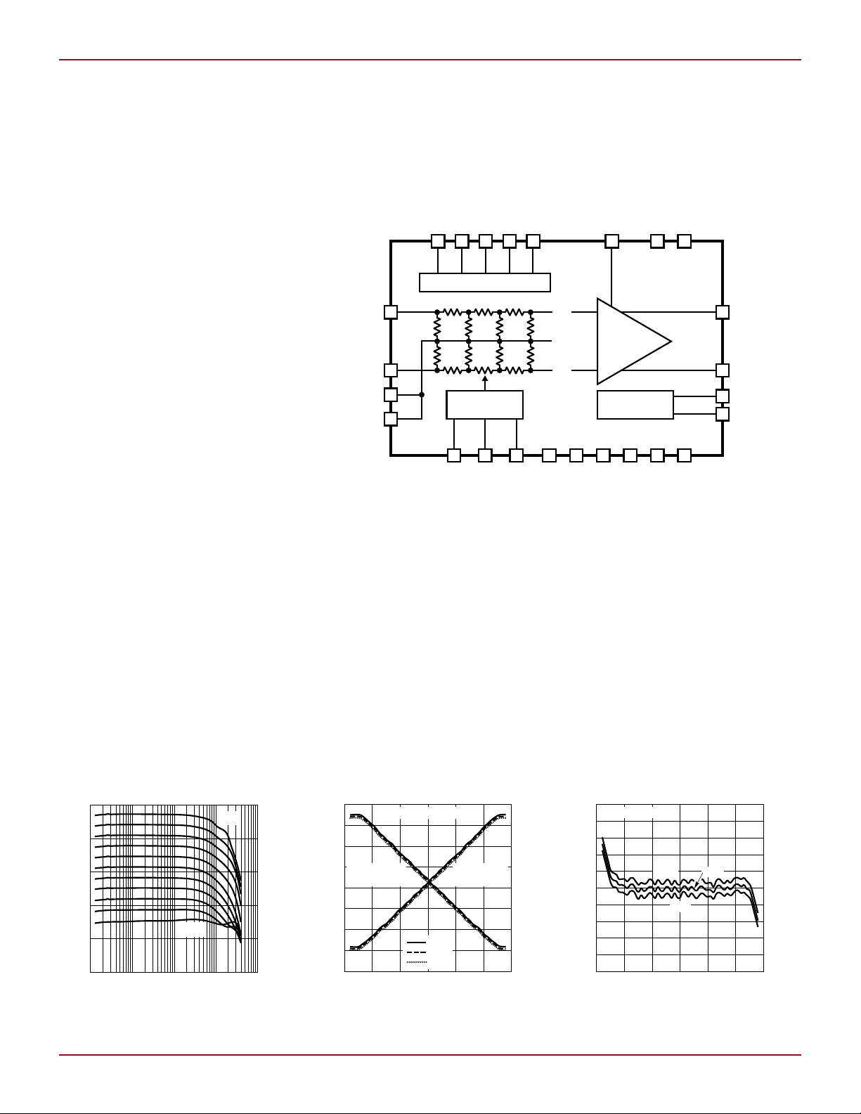
Figure 1. Block diagram of the LTC6412
by Walter Strifler
tally controlled VGA. While this trend
statement is largely true, it overlooks
important distinctions between the
two types of VGA control.
The digitally controlled VGA is
a natural choice when the system
parameters that determine optimum
gain are known to the digital control
system and are readily available across
a data bus. This information is piped
to the data inputs of the VGA, and the
desired gain is step-adjusted during
noncritical periods in the time-slotted
signal.
The digital control scenario is the
goal of most system designs, but
it leaves many application gaps for
Figure 2. LTC6412 gain vs frequency over gain
control range
Linear Technology Magazine • September 2009
Figure 3. Differential gain vs control voltage
over temperature for the LTC6412
Figure 4. LTC6412 gain conformance error vs
control voltage over temperature
19
L DESIGN FEATURES
RF
OUT
50Ω
PEAK
RF
OUT
= 4dBm
–V
G
0.5V/DIV
0.5µs/DIV
V
CC
GND
SHDNEN
–V
G
V
REF
+V
G
–OUT
+OUT
–OUT
+OUT
–IN
+IN
–IN
+IN
10nF
10nF
10nF
C
F
1000pF
10nF
IF IN IF OUT
–IN
+IN
LTC6412 LTC6400-8
LT5537
V
CC
EN
GND
220Ω
10nF
2.2nF
470pF
10nF
1k 1k1k 1k
180nH 180nH
3.3V
3.3V
3.3V
3.3V
3.3V
3.3V
–
+
½LTC6244
590k
33k
2k
100Ω
AGC SET
–20dB TAP
0.1µF
OUT
INPUT
200mV/DIV
OUTPUT
200mV/DIV
20µs/DIV
INPUT
200mV/DIV
C=330pF
C=1000pF
C=4400pF
20µs/DIV
OUTPUT (200mV/DIV)
clever analog solutions. For example,
what if the information needed to
control the amplifier gain is not known
to the digital control system or no
practical data bus is available? What
if the RF signal through the amplifier chain cannot tolerate any step
disturbance in amplitude or phase?
These kinds of situations arise often
enough to sustain a healthy market
for analog-controlled VGAs. A few
such applications are discussed later
in this article.
Design Features
The LTC6412 is an 800MHz analogcontrolled VGA manufactured on an
advanced silicon-germanium (SiGe)
BiCMOS process that offers the speed
and performance of a complementary
SiGe bipolar process along with the
flexibility and compactness of a CMOS
process. The term SiGe refers to the
material composition of the bipolar
base layers whereby a SiGe semiconductor alloy is used to create critical
bandgap discontinuities and drift
fields within the bipolar devices to
improve high speed performance.
Figure 5. LTC6412 gain control 10dB step
response at IF = 70MHz
Figure 1 shows a block diagram of
the LTC6412. The design employs an
interpolated, tapped attenuator circuit
architecture to generate the variable
gain characteristic of the amplifier.
The tapped attenuator is fed to a
buffer and output amplifier to complete the differential signal path. The
circuit architecture provides good RF
input handling capability along with
a constant output noise and output
IP3 characteristic that are desirable for
most IF signal chain applications.
The internal circuitry takes the gain
control signal from the ±VG terminals
and converts this to an appropriate set
of control signals to the attenuator lad-
der. The attenuator control preserves
OIP3 through the interpolated transitions and ensures that the linear-in-dB
gain response is continuous and
monotonic over the 31dB gain range
for both slow and fast moving input
control signals, all while maintaining a
fixed input and output terminal impedance. The control terminal inputs can
be configured for positive or negative
gain slope mode by connecting the
unused control terminal to the V
REF
pin provided.
The output amplifier employs an
open-collector topology and linearizing
techniques similar to the LT5554. Enhanced clamping circuits provide fast
overdrive recovery up to 15dB signal
compression. The entire circuit runs
off a 3.3V supply at a nominal total
supply current of 110mA.
Electrical Performance
The LTC6412 is a fully differential VGA
designed for AC-coupled operation in
signal chains from 1MHz–500MHz and
provides a typical maximum gain of
17dB and minimum noise figure (NF)
of 10dB over this frequency range.
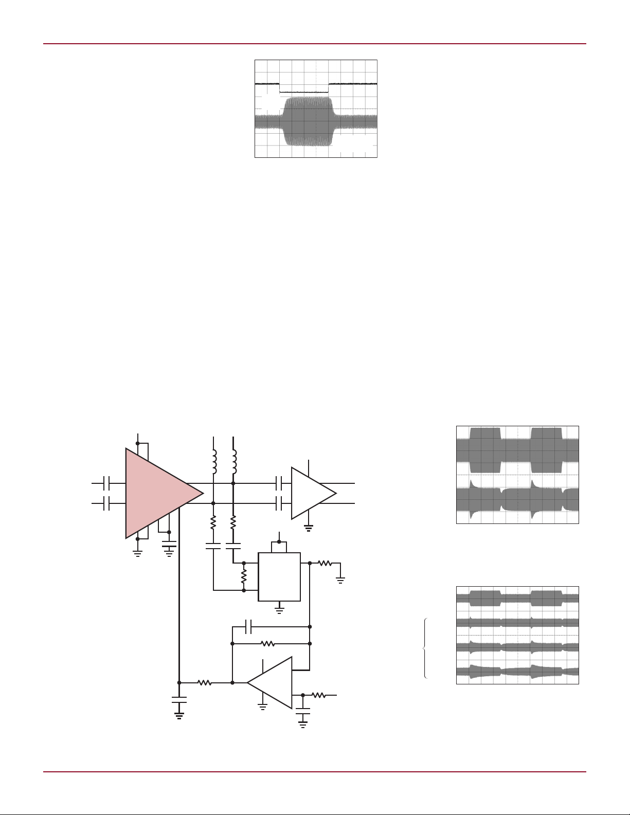
Figure 6. Analog control loop application circuit at IF = 240MHz. LTC6412 bypass capacitors to
ground omitted for clarity.
20
Figure 7. Measured analog control loop circuit
response to 6dB step changes in input signal
amplitude for CF = 1000pF
Figure 8. Measured analog control loop
response to 6dB step changes in input signal
amplitude over a range of CF values
Linear Technology Magazine • September 2009

DESIGN FEATURES L
GAIN AT 70MHz (dB)
TEMPERATURE (°C)
100–60
20
–15
–40 –20 0 20 40 60 80
15
10
5
0
–5
–10
POT R1: SLOPE ADJUST
POT R2: GAIN ADJUST
0.080dB/°C
0.064dB/°C
0.048dB/°C
0.032dB/°C
0.016dB/°C
TO LTC6412
–VGPIN
0.1µF
0.1µF
3.3V
3.3V
R
2
GAIN
100k
100k
390k
200k
10k30k
MAXMIN
–
+
½LTC6078
R
1
SLOPE
100k
MAX
MIN
10mV/°C
TEMPERATURE
SENSOR
V
CC
GND
SHDNEN
–V
G
V
REF
+V
G
–OUT
+OUT
–IN
+IN
10nF
10nF
10nF
10nF
IF IN
–IN
+IN
LTC6412 DRIVER AMP
BASEBAND
PROCESSOR
10pF
2.2nF
10pF
33nH 33nH
3.3V
3.3V
3.3V
3.3V
3.3V
1k
DIGITAL
AGC
CONTROL
DATA
OUT
0.1µF
3.3V
ADC
8-BIT DAC
LTC2640-8
SPI BUS
1k
Figure 9. Digital control loop application circuit at IF = 240MHz. LTC6412 bypass capacitors to ground omitted for clarity.
At a typical operating intermediate
frequency (IF) of 240MHz, the part
delivers a constant OIP3 = 35dBm
and constant (IIP-NF) = 8dBm over
the –14dB to +17dB gain range. The
flat output noise (NF + Gain) and flat
OIP3 combination produces a uniform
spurious-free dynamic range (SRDR) >
120dB over the full gain control range
at 240MHz. The data sheet describes
the operating performance in more
detail, but a few excerpts are worth
noting here.
Figure 2 illustrates the gain vs frequency performance of the LTC6412.
Uniform gain slope and spacing are
maintained throughout the gain
control range and across the recommended operating frequency range.
Figure 3 illustrates the gain control response to the ±VG inputs. The
linear-in-dB response is accurately
maintained throughout the gain con-
trol range with an RMS error ripple
of approximately 0.1dB as depicted
in Figure 4.
Figure 5 illustrates a typical gain
step response. The settling time of
400ns is smooth and roughly independent of the step size. The phase
change is also continuous through
any step and typically less than 5° for
signals of 240MHz or lower.
Typical Applications
Analog AGC
Automatic gain control (AGC) is usually the first application that comes to
mind for an analog-controlled VGA.
The idea is to use the linear-in-dB
VGA together with a linear-in-dB
detector to form a servo control loop
that automatically adjusts the signal
amplitude to a set level. An example of
such a control loop is shown in Figure
6. The loop gain of 100 provides an AGC
accuracy of a few tenths of a dB, and
the dominant pole compensation from
CF = 1000pF provides a well-damped
response time of 15µs shown in Figure 7. Adjusting CF over a 13:1 range
produces a similar proportional range
in settling time (see Figure 8).
The analog gain control loop is an
attractive solution for simple signals.
The linear-in-dB nature of both the
VGA and detector produces control
dynamics that are constant and linear
throughout the control range. The
detector shown in the example is a
peak detector, but an RMS detector
can also be used.
Digital AGC
The analog gain control loop is less
attractive for 3G and 4G communication signals with a high crest factor
continued on page 30
Figure 10. Application circuit for static gain adjust and temperature gain slope compensation
using a PTAT temperature sensing IC. Adjust R1 and R2 as needed and route output to –VG
control terminal of the LTC6412.
Linear Technology Magazine • September 2009
Figure 11. Gain vs temperature performance
characteristics of the PTAT sensor based
circuit shown in Figure 10
21

L DESIGN IDEAS
GAIN AT 70MHz (dB)
TEMPERATURE (°C)
100–60
20
–15
–40 –20 0 20 40 60 80
15
10
5
0
–5
–10
POT R1: SLOPE ADJUST
POT R2: GAIN ADJUST
0.080dB/°C
0.064dB/°C
0.048dB/°C
0.032dB/°C
0.016dB/°C
TO
LTC6412
–VGPIN
0.1µF
0.1µF
3.3V
3.3V
3.3V
R
1
SLOPE
100k
100k
100k
12k
20k
14k
20k
390k
MAXMIN
–
+
½LTC6078
R
2
GAIN
100k
MAX
MIN
20k
68k
NTC
also be adjusted by applying a single
resistor from ADJ to ground, as shown
in Figure 3.
The PWM control pin allows high
dimming ratios. With an external
MOSFET in series with the LED string
Figure 6. Only 9mm × 15mm × 4.32mm, the LTM8040
LED Driver is a complete system in an LGA package
LTC6412, continued from page 21
as shown in Figure 4, the LTM8040
can achieve dimming ratios in excess
of 250:1. As seen in Figure 5, there
is little distortion of the PWM LED
current, even at frequencies as low as
10Hz. The 10Hz performance is shown
because the control target is often
more complicated than a simple peak
or RMS amplitude, and the amplitude
noise introduced by the analog control
loop may be unacceptable. A common
solution for these systems is an analog
VGA driven by a DAC as depicted in
Figure 9.
The contradiction of a DAC controlling an analog-controlled VGA may
appear at first as unusual and unecessary, but the arrangement provides
key benefits. The gain step resolution is
not determined by the VGA, and 8–12
bit DAC’s are relatively inexpensive.
More importantly, the signal gain can
be adjusted with arbitrary smooth-
Figure 12. Thermistor-based application
circuit for static gain adjust and temperature
gain slope compensation. Adjust R1 and R2
as needed and route output to –VG control
terminal of the LTC6412.
ness, so the baseband processor can
continue its demodulation/decoding
operation without interruption. Most
digital VGAs produce unacceptable
signal discontinuities. The DAC does
have a glitch of its own, but it is a
baseband glitch that can be smoothed
with filters. The glitch in many digital
VGAs has no such remedy.
Gain and Temperature
Compensation
Many communication receivers require frequent gain optimization, but
others are designed with over-performing ADCs that can tolerate moderate
signal amplitude variation and avoid
much of the AGC hardware problem.
However, even these “fixed gain”
system blocks often require a gain
30
30
adjustment to compensate gain drift
overtemperature and any cumulative
gain tolerance of the other components. Several system components are
cascaded to form a chain that usually
includes a VGA to perform a one-time
adjustment of gain and temperature
slope to compensate the tolerances and
slopes of the other components. In this
scenario, the required temperature
and compensation information is not
known to the baseband processor or
it is impractical to send this data to a
suitably located VGA.
natural solution for this application
because it can easily interpret the output of most temperature transducers
without digitization. Figure 10 shows
An analog-controlled VGA is a
to illustrate the capabilities of the
LTM8040—this frequency is too low
for practical pulse width modulation,
being well within the discrimination
range of the human eye.
The LTM8040 also features a low
power shutdown state. When the
SHDN pin is active low, the input
quiescent current is less than 1µA.
Conclusion
The LTM8040 µModule LED driver
makes it easy to drive LEDs. Its high
level of integration and rich feature set,
including open LED protection, analog
and PWM dimming, save significant
design time and board space.
Figure 13. Gain vs temperature performance
characteristics of the thermistor-based circuit
shown in Figure 12
L
a simple application circuit using a
common PTAT temperature sensor
and an op amp to create the required
–VG signal to adjust room temperature
gain and temperature slope as shown
in Figure 11. If temperature slope
accuracy is only important for T >
0°C, then the same function can be
performed with an inexpensive NTC
thermistor as shown in Figures 12 and
13. Trying doing that with a digitally
controlled VGA!
Conclusion
By combining the advanced SiGe
process with an innovative design, the
LTC6412 offers unparalleled analog
VGA performance at 3.3V. The tiny
16mm² leadless package and minimal
external components produce a cost
effective, fully differential VGA solution
in less than 1cm² of PCB area.
Linear Technology Magazine • September 2009
L
 Loading...