

Using a Differential I/O Amplifi er in Single-Ended Applications
Design Note DN473
Glen Brisebois
Introduction
Recent advances in low voltage silicon germanium
and BiCMOS processes have allowed the design and
production of very high speed amplifi ers. Because the
processes are low voltage, most of the amplifi er designs
have incorpora ted different ial inputs and outputs to re gain
and maximize total output signal swing. Since many lowvoltage applic ations are single-ended, the quest ions arise,
“How can I use a dif ferential I/O ampli fi er in a single-ended
application?” and “What are the implications of such
use?” This Design Note addresses some of the practical
implications and demonstrates specifi c single-ended
applications using the 3GHz gain-bandwidth LTC6406
differential I/O amplifi er.
Background
A conventional op amp has two differential inputs and
an output. The gain is nominally infi nite, but control
is maintained by virtue of feedback from the output
to the negative “inverting” input. The output does not
go to infi nity, but rather the differential input is kept to
zero (divided by infi nity, as it were). The utility, variety
and beauty of conventional op amp applications are
well documented, yet still appear inexhaustible. Fully
differential op amps have been less well explored.
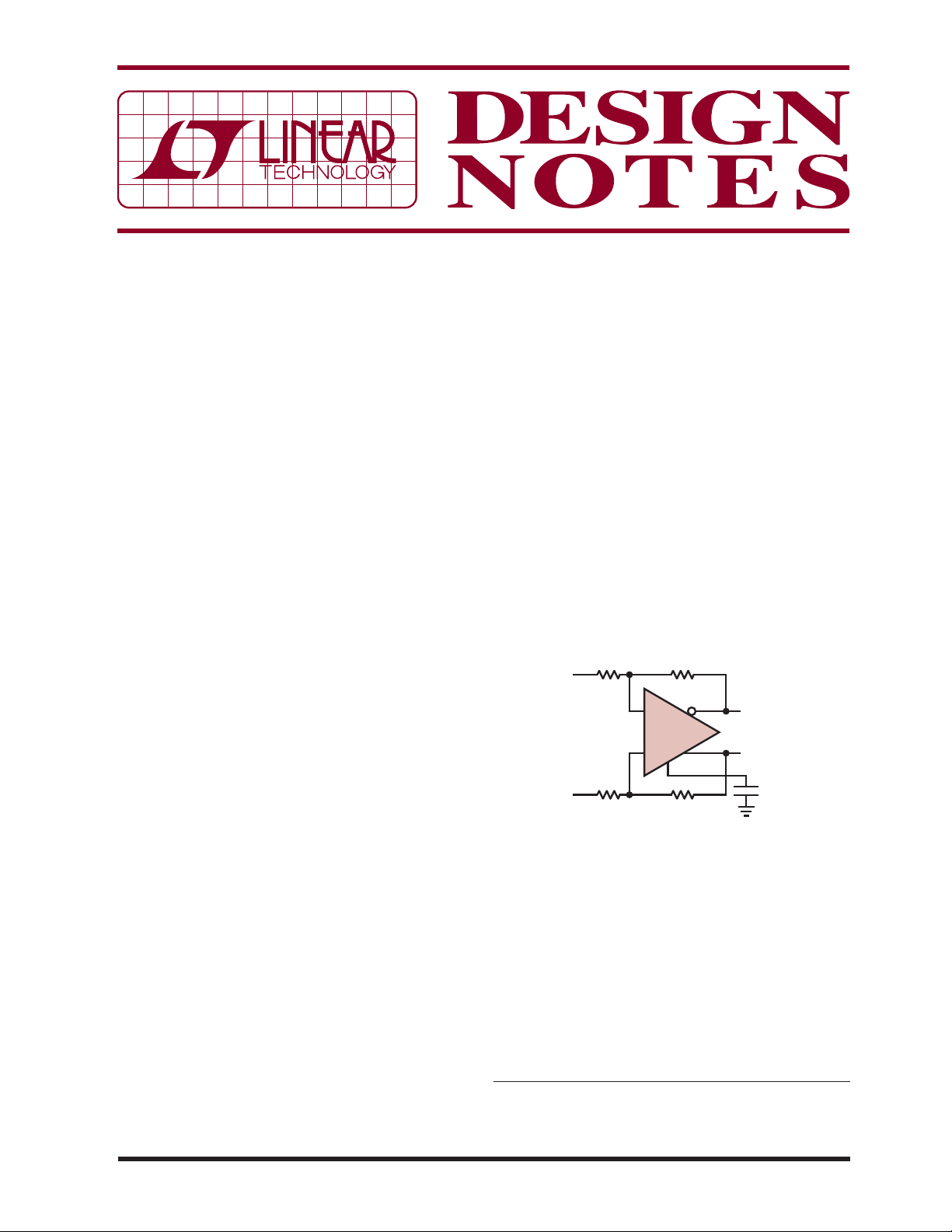
Figure 1 shows a differential op amp with four feedback
r e s i s t o r s . I n t h i s c a s e t h e d i f f e r e n t i a l g a i n i s s t i l l n o m i n a l l y
infi nite, and the inputs kept together by feedback, but
this is not adequate to dictate the output voltages. The
reason is that the common mode output voltage can be
anywhere and still result in a “zero” differential input
voltage bec ause the feedback is symmetric. T herefore, for
any fully differential I/O amplifi er, there is always another
control voltage to dictate the output common mode
voltage. This is the purpose of the V
pin, and explains
OCM
why fully differential amplifi ers are at least 5-pin devices
(not including supply pins) rather than 4-pin devices. The
differential gain equation is V
OUT(DM)
= V
IN(DM)
• R2/R1.
The common mode output voltage is forced internally to
the voltage applied at V
. One fi nal observation is that
OCM
there is no longer a single inverting input: both inputs are
inverting and noninverting depending on which output
is considered. For the purposes of circuit analysis, the
inputs are labeled with “+” and “–” in the conventional
manner and one output receives a dot, denoting it as the
inverted output for the “+” input.
Anybody familiar with conventional op amps knows that
noninverting applications have inherently high input
impedance at the noninverting input, approaching GΩ or
even TΩ. But in the case of the fully differential op amp
in Figure 1, there is feedback to both inputs, so there is
no high impedance node. Fortunately this diffi culty can
be overcome.
RI2
V
IN
RI1
Figure 1. Fully Differential I/O Amplifi er Showing Two
Outputs and an Additional V
+
LTC6406
–
RF2
V
OCM
RF1
OCM
Pin
V
OUT
V
OUT
–
+
0.1μF
DN4GB F01
Simple Single-Ended Connection of a Fully
Differential Op amp
Figure 2 shows the LTC640 6 connected as a single-ended
op amp. Only one of the outputs has been fed back and
only one of the inputs receives feedback. The other input
is now high impedance. The LTC6406 works fi ne in this
circuit and still provides a differential output. However, a
simple thought experiment reveals one of the downsides
L, LT, LTC, LTM, Linear Technology, the Linear logo and μModule are registered
trademarks of Linear Technology Corporation. All other trademarks are the property of
their respective owners.
12/09/473
of this confi guration. Imagine that all of the inputs and
outputs are sitting at 1.2V, including V
that the V
only ou tpu t tha t can move is V
remain equal to V
pin is driven an addi tional 0.1V higher. The
OCM
, so in order to move the common
IN
OUT
–
. Now imagine
OCM
because V
OUT
+
must
mode output higher by 100mV the amplifi er has to move
–
the V
differential output shift due to a 100mV V
output a total of 200mV higher. That’s a 200mV
OUT
OCM
shift. This
illustrates the fact that single-ended feedback around a
fully differential amplifi er introduces a noise gain of two
from the V
pin to the “open” output. In order to avoid
OCM
this noise, simply do not use that output, resulting in a
fully single-ended application. Or, you can take the slight
noise penalty and use both outputs.
–
V
IN
+
LTC6406
–
V
OCM
V
OUT
+
V
OUT
0.2pF
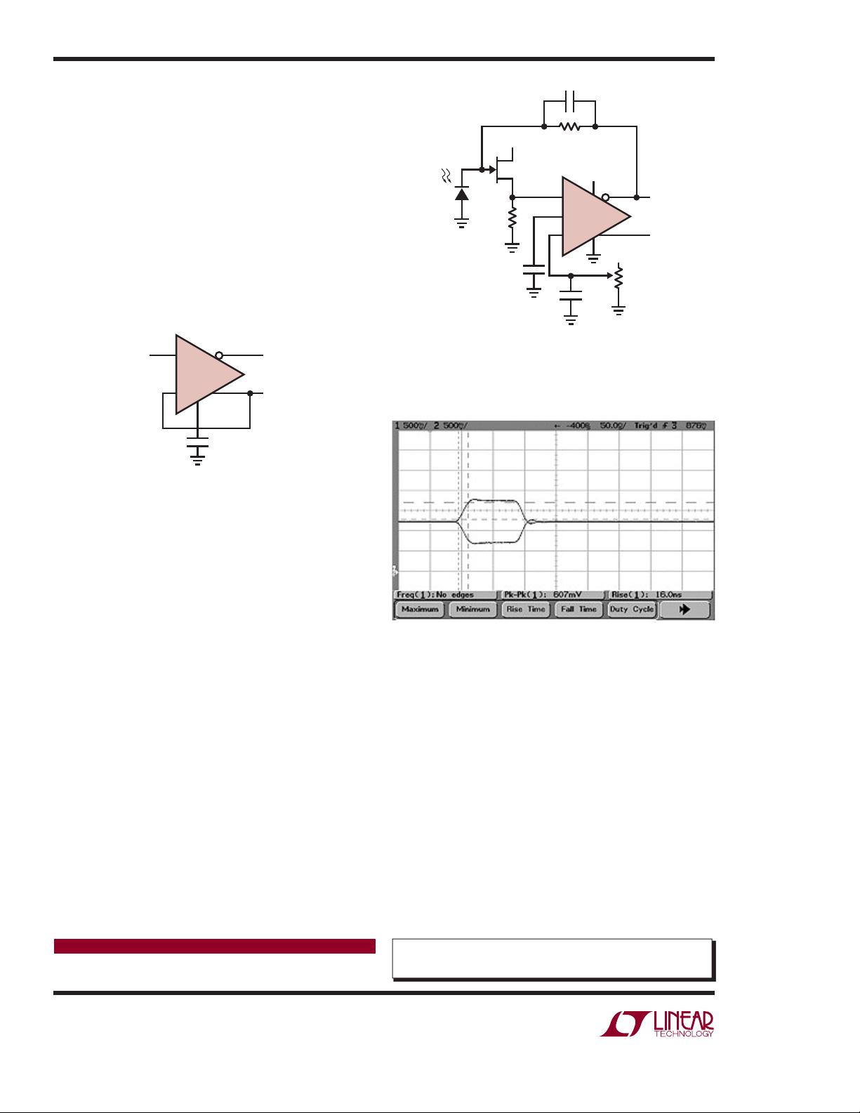
NXP
BF862
V
OCM
0.1μF
20k 1%
+
LTC6406
–
3V
–
V
OUT
+
V
OUT
3V
10k
DN4GB F03
OSRAM
SFH213
3V
715
0.1μF
Figure 3. Transimpedance Amplifi er. Ultralow Noise JFET
Buffers the Current Noise of the Bipolar LTC6406 Input
Trim the Pot for 0V Differential Output under No-Light
Conditions.
0.1μF
DN4GB F02
Figure 2. Feedback Is Single-Ended Only. This Circuit Is
Stable, with a Hi-Z Input Like the Conventional Op Amp.
The Closed Loop Output (V
+
in This Case) Is Low Noise.
out
Output Is Best Taken Single-Ended from the Closed Loop
Output, Providing a 3db Bandwidth Of 1.2ghz. The Open
Loop Output (V
–
) Has a Noise Gain Of Two From V
out
ocm
,
But Is Well Behaved to About 300mhz, Above Which It Has
Signifi cant Passband Ripple.
A Single-Ended Transimpedance Amplifi er
Figure 3 shows the LTC640 6 connected as a single-ended
transimpedance amplifi er with 20kΩ of transimpedance
gain. The BF862 JFET buffers the LTC6406 input,
drastically reducing the effects of its bipolar input
transistor current noise. The V
of the JFET is now
GS
included as an of fset, but this is t ypically 0.6V so the circuit
still functions well on a 3V single supply and the offset
can be dialed out with the 10k potentiometer. The time
dom ai n r esp on se is sh ow n in Fi gu re 4. Tot al ou tp ut n oi se
on 20MHz bandwidth measurements shows 0.8mV
on V
+
and 1.1mV
OUT
RMS
on V
–
. Taken differentially,
OUT
RMS
the transimpedance gain is 40kΩ.
Figure 4. Time Domain Response of Circuit of Figure 3,
Showing Both Outputs Each with 20kΩ of TIA Gain. Rise
Time is 16ns, Indicating a 20MHz Bandwidth.
Conclusion
New families of full y differential op amps like the LTC6406
offer unprecedented bandwidths. Fortunately, these
op amps can also function well in single-ended and 100%
feedback applications.
Data Sheet Download
www.linear.com
Linear Technology Corporation
1630 McCarthy Blvd., Milpitas, CA 95035-7417
(408) 432-1900
●
FAX: (408) 434-0507 ● www.linear.com
For applications help,
call (408) 432-1900, Ext. 3755
dn473 LT/TP 1209 116K • PRINTED IN THE USA
© LINEAR TECHNOLOGY CORPORATION 2009
 Loading...