

FEATURES
–
LTC6240/LTC6241/LTC6242
Single/Dual/Quad 18MHz,
Low Noise, Rail-to-Rail Output,
CMOS Op Amps
U
DESCRIPTIO
■
0.1Hz to 10Hz Noise: 550nV
■
Input Bias Current:
P-P
0.2pA (Typ at 25°C)
1pA Max (LT6240)
■
Low Offset Voltage: 125µV Max
■
Low Offset Drift: 2.5µV/°C Max
■
Gain Bandwidth Product: 18MHz
■
Output Swings Rail-to-Rail
■
Supply Operation:
2.8V to 6V LTC6240/LTC6241/LTC6242
2.8V to ±5.5V LTC6240HV/LTC6241HV/LTC6242HV
■
Low Input Capacitance
■
H Grade Temperature Range: –40°C to 125°C
■
Single LTC6240 in 5-Pin SOT-23 Package and
8-Pin SO for PCB Guard Ring
■
Dual LTC6241 in 8-Pin SO and Tiny DFN Packages
■
Quad LTC6242 in 16-Pin SSOP and 5mm × 3mm
DFN Packages
U
APPLICATIO S
■
Photo Diode Amplifi ers
■
Charge Coupled Amplifi ers
■
Low Noise Signal Processing
■
Medical Instrumentation
■
High Impedance Transducer Amplifi er
The LTC®6240/6241/LTC6242 are single, dual and quad
low noise, low offset, rail-to-rail output, unity gain stable
CMOS op amps that feature 1pA of input bias current. Input
bias current is guaranteed to be 1pA max on the single
LTC6240. The 0.1Hz to 10Hz noise of only 550nV
, along
P-P
with an offset of just 125µV are signifi cant improvements
over traditional CMOS op amps. Additionally, noise is
guaranteed to be less than 10nV/√Hz at 1kHz. An 18MHz
gain bandwidth, and 10V/µs slew rate, along with the wide
supply range and low input capacitance, make them perfect
for use as fast signal processing amplifi ers.
These op amps have an output stage that swings within
30mV of either supply rail to maximize the signal dynamic
range in low supply applications. The input common mode
range extends to the negative supply. They are fully specifi ed on 3V and 5V, and an HV version guarantees operation
on supplies up to ±5V.
The LTC6240 is available in the 8-pin SO and the 5-pin
SOT-23 packages. The LTC6241 is available in the 8-pin
SO, and for compact designs it is packaged in a tiny dual
fi ne pitch leadless (DFN) package. The LTC6242 is available in the 16-Pin SSOP as well as the 5mm × 3mm DFN
package.
, LTC and LT are registered trademarks of Linear Technology Corporation.
All other trademarks are the property of their respective owners.
U
TYPICAL APPLICATIO
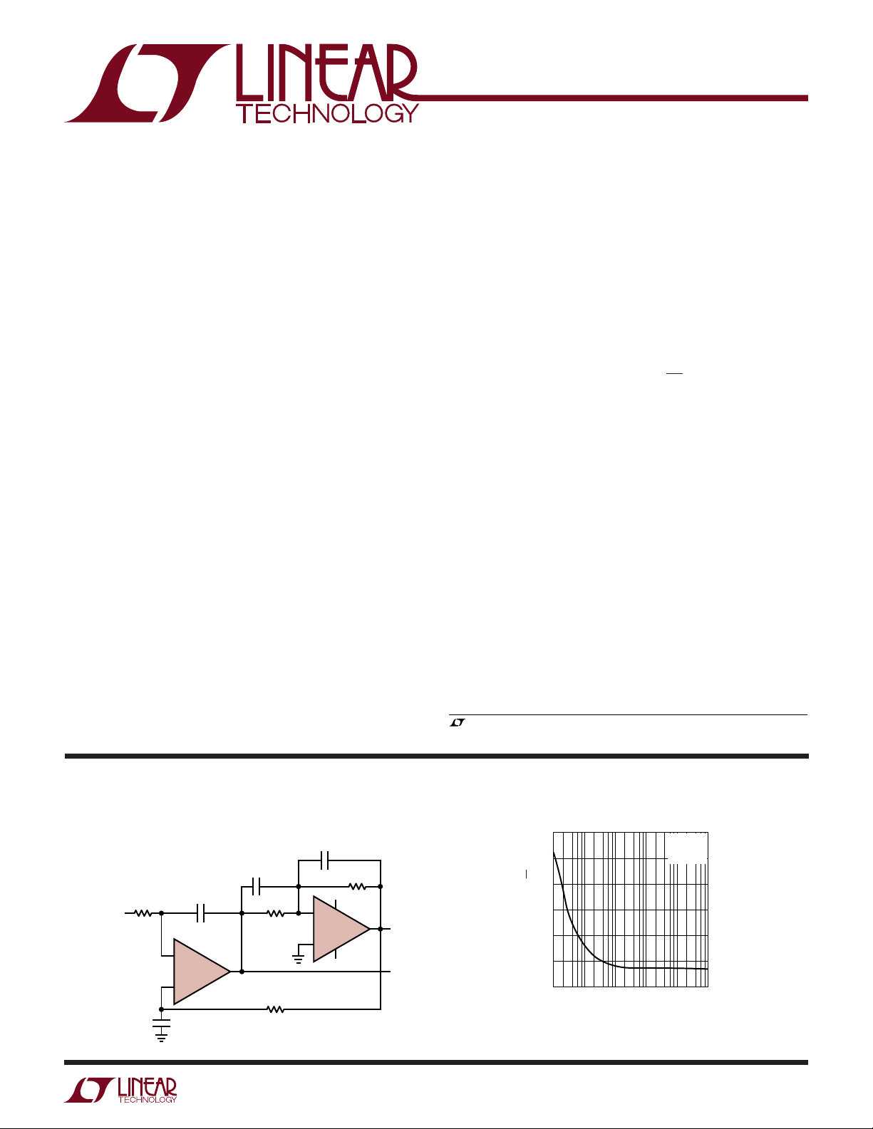
Low Noise Single-Ended Input to Differential Output Amplifi er
C3
10pF
C4
10pF
–
LTC6241
+
10pF
1/2
C1
R3
4.99k
R2
200k
R1
200k
V
IN
C2
10pF
+2.5V
–
LTC6241
+
–2.5V
R4
4.99k
1/2
6241 TA01a
Noise Voltage vs Frequency
60
50
40
30
+
V
OUT
V
OUT
20
NOISE VOLTAGE (nV/√Hz)
10
0
10
1 100 1k 100k
FREQUENCY (Hz)
TA = 25°C
= ±2.5V
V
S
= 0V
V
CM
10k
6241 TA01b
624012fc
1
LTC6240/LTC6241/LTC6242
WW
W
ABSOLUTE AXI U RATI GS
U
(Note 1)
Total Supply Voltage (V+ to V–)
LTC6240/LTC6241/LTC6242 ...................................7V
LTC6240HV/LTC6241HV/LTC6242HV ...................12V
+
Input Voltage .......................... (V
+ 0.3V) to (V– – 0.3V)
Input Current ........................................................±10mA
Output Short Circuit Duration (Note 2) ............ Indefi nite
Operating Temperature Range
LTC6240C/LTC6241C/LTC6242C .......... –40°C to 85°C
LTC6240I/LTC6241I/LTC6242I .............–40°C to 85°C
LTC6240H/LTC6241H/LTC6242H .......–40°C to 125°C
UUW
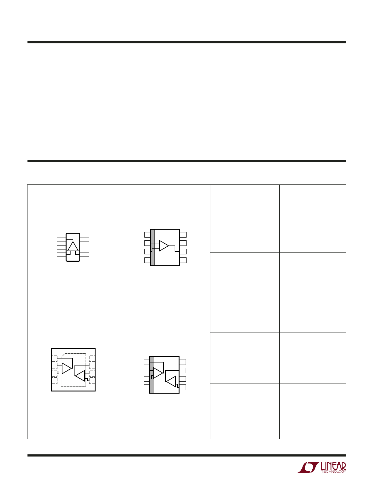
PACKAGE/ORDER I FOR ATIO
TOP VIEW
OUT 1
–
V
2
+
+IN 3
5-LEAD PLASTIC TSOT-23
T
= 150°C, θJA = 250°C/W
JMAX
–
S5 PACKAGE
5 V
4 –IN
+
NC
–IN
+IN
V
TOP VIEW
1
–
2
+
3
–
4
S8 PACKAGE
8-LEAD PLASTIC SO
T
= 150°C, θJA = 190°C/W
JMAX
Specifi ed Temperature Range (Note 3)
LTC6240C/LTC6241C/LTC6242C .............. 0°C to 70°C
LTC6240I/LTC6241I/LTC6242I .............–40°C to 85°C
LTC6240H/LTC6241H/LTC6242H .......–40°C to 125°C
Junction Temperature ........................................... 150°C
DHC, DD Package ............................................. 125°C
Storage Temperature Range ....................–65ºC to 150°C
DHC, DD Package ...............................–65ºC to 125°C
Lead Temperature (Soldering, 10 sec) .................. 300°C
ORDER PART NUMBER S5 PART MARKING*
LTC6240CS5
LTC6240HVCS5
LTC6240IS5
8
NC
+
V
7
OUT
6
NC
5
LTC6240HVIS5
LTC6240HS5
LTC6240HVHS5
ORDER PART NUMBER S8 PART MARKING
LTC6240CS8
LTC6240HVCS8
LTC6240IS8
LTC6240HVIS8
LTC6240HS8
LTC6240HVHS8
LTCRR
LTCRS
LTCRR
LTCRS
LTCRR
LTCRS
6240
6240HV
6240I
240HVI
6240H
240HVH
TOP VIEW
1OUT A
–IN A
2
+IN A
V
8-LEAD (3mm × 3mm) PLASTIC DFN
UNDERSIDE METAL CONNECTED TO V
A
3
–
4
DD PACKAGE
T
= 125°C, θJA = 43°C/W
JMAX
(PCB CONNECTION OPTIONAL)
2
ORDER PART NUMBER DD PART MARKING*
LTC6241CDD
+
8
V
OUT B
7
–IN B
6
B
+IN B
5
–
OUT A
–IN A
+IN A
V
TOP VIEW
1
2
A
3
–
4
S8 PACKAGE
8-LEAD PLASTIC SO
T
= 150°C, θJA = 190°C/W
JMAX
+
8
V
OUT B
7
–IN B
6
B
+IN B
5
LTC6241HVCDD
LTC6241IDD
LTC6241HVIDD
ORDER PART NUMBER S8 PART MARKING
LTC6241CS8
LTC6241HVCS8
LTC6241IS8
LTC6241HVIS8
LTC6241HS8
LTC6241HVHS8
LBPD
LBRR
LBPD
LBRR
6241
6241HV
6241I
241HVI
6241H
241HVH
624012fc
UUW
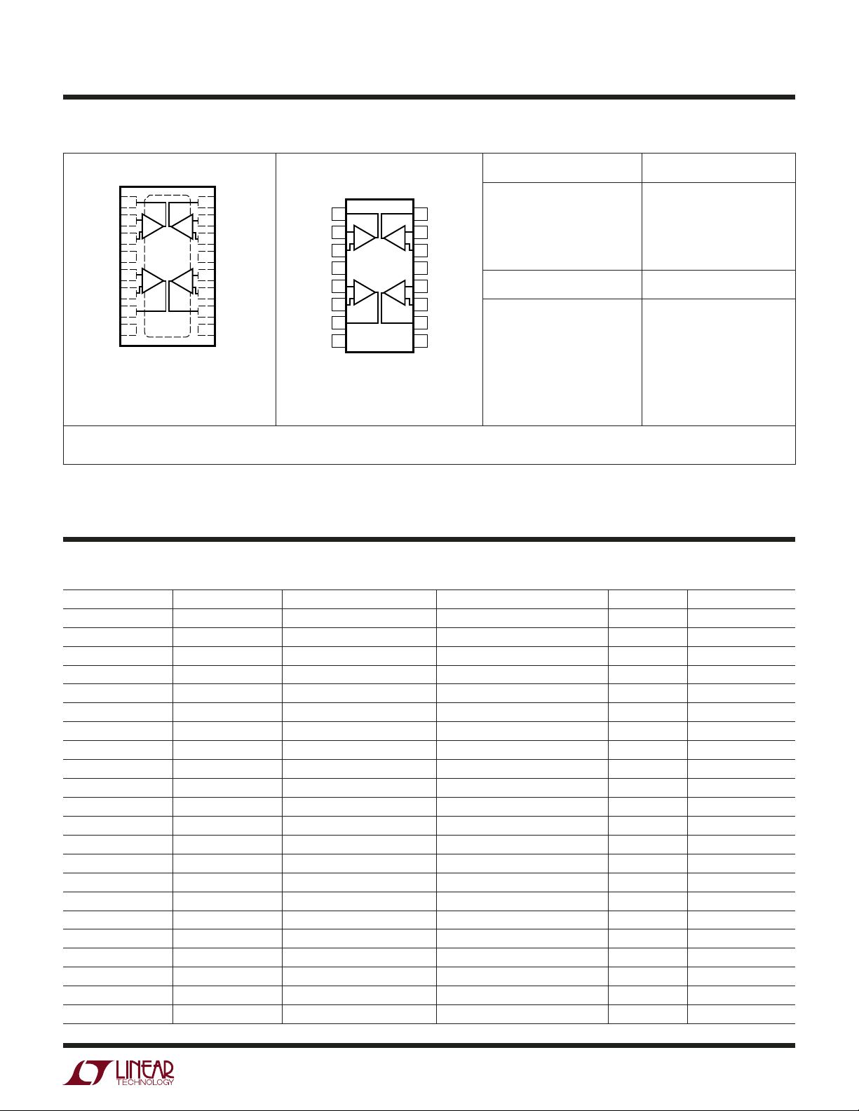
PACKAGE/ORDER I FOR ATIO
LTC6240/LTC6241/LTC6242
TOP VIEW
OUT A
1
–IN A
2
+IN A
V
+IN B
–IN B
OUT B
NC
16-LEAD (5mm × 3mm) PLASTIC DFN
UNDERSIDE METAL CONNECTED TO V
A
3
+
4
5
B
6
7
8
DHC16 PACKAGE
T
= 125°C, θJA = 43°C/W
JMAX
(PCB CONNECTION OPTIONAL)
16
OUT D
15
–IN D
D
14
+IN D
–
13
17
V
+IN C
12
C
–IN C
11
OUT C
10
NC
9
TOP VIEW
1
OUT A
2
–IN A
+IN A
V
+IN B
–IN B
OUT B
NC
–
A
3
+
4
5
B
6
7
8
GN PACKAGE
16-LEAD PLASTIC SSOP
T
= 150°C, θJA = 135°C/W
JMAX
OUT D
16
–IN D
15
D
+IN D
14
–
V
13
+IN C
12
C
–IN C
11
OUT C
10
NC
9
ORDER PART NUMBER DHC PART MARKING*
LTC6242CDHC
LTC6242HVCDHC
LTC6242IDHC
LTC6242HVIDHC
6242
6242HV
6242
6242HV
ORDER PART NUMBER GN PART MARKING
LTC6242CGN
LTC6242HVCGN
LTC6242IGN
LTC6242HVIGN
LTC6242HGN
LTC6242HVHGN
6242
6242HV
6242I
242HVI
6242H
242HVH
Order Options Tape and Reel: Add #TR Lead Free: Add #PBF Lead Free Tape and Reel: Add #TRPBF
Lead Free Part Marking: http://www.linear.com/leadfree/
*The temperature grade is identifi ed by a label on the shipping container. Consult LTC Marketing for parts specifi ed with wider operating temperature ranges.
U
AVAILABLE OPTIO S
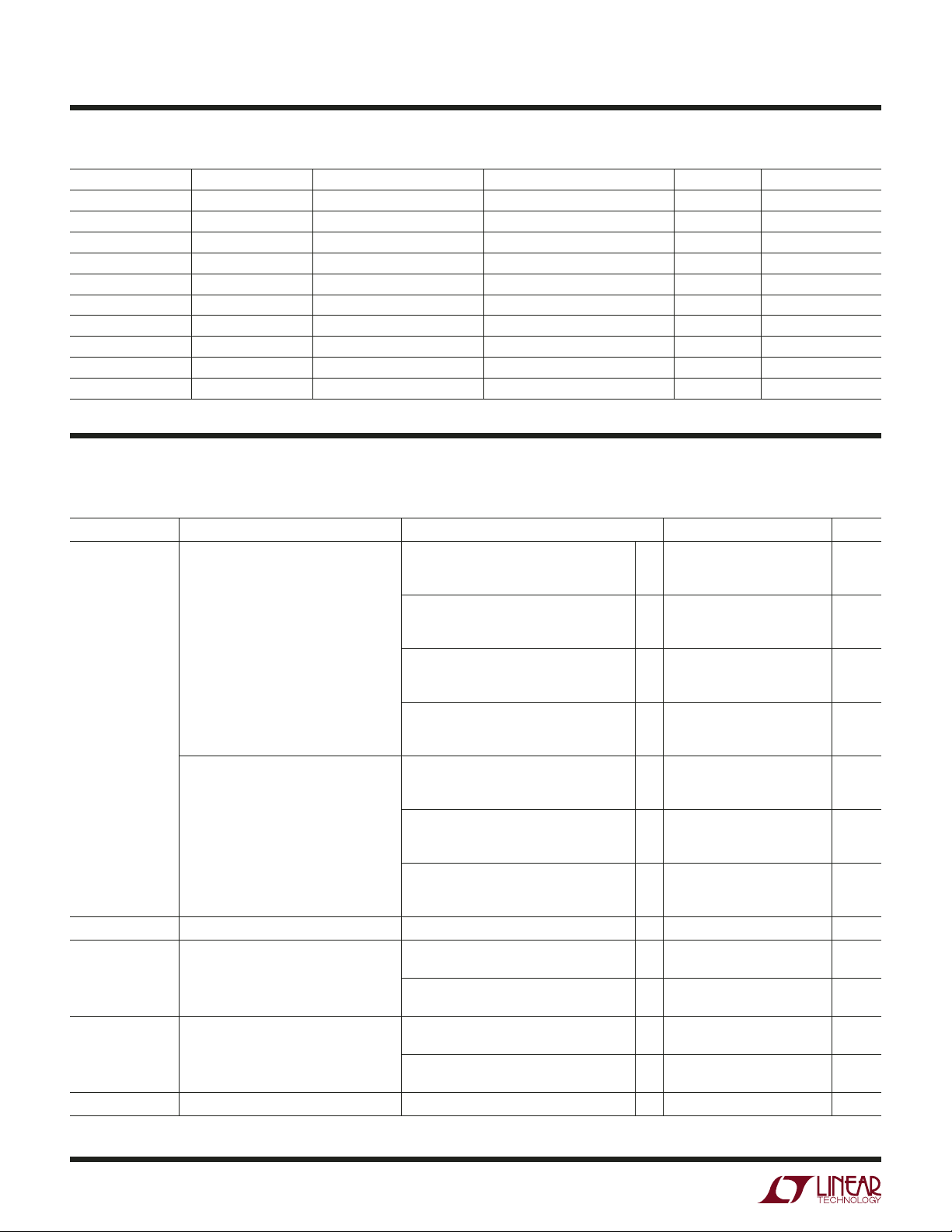
PART NUMBER AMPS/PACKAGE SPECIFIED TEMP RANGE SPECIFIED SUPPLY VOLTAGE PACKAGE PART MARKING
LTC6240CS5 1 0°C to 70°C 3V, 5V SOT-23 LTCRR
LTC6240CS8 1 0°C to 70°C 3V, 5V SO-8 6240
LTC6240HVCS5 1 0°C to 70°C 3V, 5V, ±5V SOT-23 LTCRS
LTC6240HVCS8 1 0°C to 70°C 3V, 5V, ±5V SO-8 6240HV
LTC6240IS5 1 –40°C to 85°C 3V, 5V SOT-23 LTCRR
LTC6240IS8 1 –40°C to 85°C 3V, 5V SO-8 6240I
LTC6240HVIS5 1 –40°C to 85°C 3V, 5V, ±5V SOT-23 LTCRS
LTC6240HVIS8 1 –40°C to 85°C 3V, 5V, ±5V SO-8 240HVI
LTC6240HS5 1 –40°C to 125°C 3V, 5V SOT-23 LTCRR
LTC6240HS8 1 –40°C to 125°C 3V, 5V SO-8 6240H
LTC6240HVHS5 1 –40°C to 125°C 3V, 5V, ±5V SOT-23 LTCRS
LTC6240HVHS8 1 –40°C to 125°C 3V, 5V, ±5V SO-8 240HVH
LTC6241CS8 2 0°C to 70°C 3V, 5V SO-8 6241
LTC6241CDD 2 0°C to 70°C 3V, 5V DD LBPD
LTC6241HVCS8 2 0°C to 70°C 3V, 5V, ±5V SO-8 6241HV
LTC6241HVCDD 2 0°C to 70°C 3V, 5V, ±5V DD LBRR
LTC6241IS8 2 –40°C to 85°C 3V, 5V SO-8 6241I
LTC6241IDD 2 –40°C to 85°C 3V, 5V DD LBPD
LTC6241HVIS8 2 –40°C to 85°C 3V, 5V, ±5V SO-8 241HVI
LTC6241HVIDD 2 –40°C to 85°C 3V, 5V, ±5V DD LBRR
LTC6241HS8 2 –40°C to 125°C 3V, 5V SO-8 6241H
LTC6241HVHS8 2 –40°C to 125°C 3V, 5V, ±5V SO-8 241HVH
624012fc
3
LTC6240/LTC6241/LTC6242
U
AVAILABLE OPTIO S
PART NUMBER AMPS/PACKAGE SPECIFIED TEMP RANGE SPECIFIED SUPPLY VOLTAGE PACKAGE PART MARKING
LTC6242CGN 4 0°C to 70°C 3V, 5V GN 6242
LTC6242CDHC 4 0°C to 70°C 3V, 5V DHC 6242
LTC6242HVCGN 4 0°C to 70°C 3V, 5V, ±5V GN 6242HV
LTC6242HVCDHC 4 0°C to 70°C 3V, 5V, ±5V DHC 6242HV
LTC6242IGN 4 –40°C to 85°C 3V, 5V GN 6242I
LTC6242IDHC 4 –40°C to 85°C 3V, 5V DHC 6242
LTC6242HVIGN 4 –40°C to 85°C 3V, 5V, ±5V GN 242HVI
LTC6242HVIDHC 4 –40°C to 85°C 3V, 5V, ±5V DHC 6242HV
LTC6242HGN 4 –40°C to 125°C 3V, 5V GN 6242H
LTC6242HVHGN 4 –40°C to 125°C 3V, 5V, ±5V GN 242HVH
(LTC6240C/I, LTC6240HVC/I, LTC6241C/I, LTC6241HVC/I, LTC6242C/I,
ELECTRICAL CHARACTERISTICS
LTC6242HVC/I) The ● denotes the specifi cations which apply over the specifi ed temperature range, otherwise specifi cations are at
TA = 25°C. VS = 5V, 0V, VCM = 2.5V unless otherwise noted.
SYMBOL PARAMETER CONDITIONS MIN TYP MAX UNITS
V
OS
TC V
I
B
I
OS
OS
Input Offset Voltage (Note 4) LTC6241 S8
V
Match Channel-to-Channel (Note 5) LTC6241 S8
OS
Input Offset Voltage Drift (Note 6)
Input Bias Current (Notes 4, 7) LTC6241, LTC6242
Input Offset Current (Notes 4, 7) LTC6241, LTC6242
Input Noise Voltage 0.1Hz to 10Hz 550 nV
0°C to 70°C
–40°C to 85°C
LTC6242 GN
0°C to 70°C
–40°C to 85°C
LTC6240
0°C to 70°C
–40°C to 85°C
LTC6241 DD, LTC6242 DHC
0°C to 70°C
–40°C to 85°C
0°C to 70°C
–40°C to 85°C
LTC6242 GN
0°C to 70°C
–40°C to 85°C
LTC6241 DD, LTC6242 DHC
0°C to 70°C
–40°C to 85°C
LTC6240
LTC6240
●
●
●
●
●
●
●
●
●
●
●
●
●
●
●
●
●
●
●
40 125
250
300
50 150
275
300
50 175
300
350
100 550
650
725
40 160
300
375
50 185
325
400
150 650
700
750
0.7 2.5 µV/°C
0.2
75
0.2 1
75
0.2
75
0.2 1
75
µV
µV
µV
µV
µV
µV
µV
µV
µV
µV
µV
µV
µV
µV
µV
µV
µV
µV
µV
µV
µV
pA
pA
pA
pA
pA
pA
pA
pA
P-P
4
624012fc
LTC6240/LTC6241/LTC6242
(LTC6240C/I, LTC6240HVC/I, LTC6241C/I, LTC6241HVC/I, LTC6242C/I,
ELECTRICAL CHARACTERISTICS
LTC6242HVC/I) The ● denotes the specifi cations which apply over the specifi ed temperature range, otherwise specifi cations are at
T
= 25°C. VS = 5V, 0V, VCM = 2.5V unless otherwise noted.
A
SYMBOL PARAMETER CONDITIONS MIN TYP MAX UNITS
e
n
i
n
R
IN
C
IN
V
CM
CMRR Common Mode Rejection 0V ≤ V
A
VOL
V
OL
V
OH
PSRR Power Supply Rejection V
I
SC
I
S
GBW Gain Bandwidth Product Frequency = 20kHz, R
SR Slew Rate (Note 11) A
FPBW Full Power Bandwidth (Note 12) V
t
s
Input Noise Voltage Density f = 1kHz 7 10 nV/√Hz
Input Noise Current Density (Note 8) 0.56 fA/√Hz
3.5
12
pF
3
pF
Input Resistance Common Mode 10
Input Capacitance
f = 100kHz
Differential Mode
Common Mode
Input Voltage Range Guaranteed by CMRR
≤ 3.5V
CM
●
0 3.5 V
●
80 105 dB
CMRR Match
Channel-to-Channel (Note 5)
●
76 95 dB
Large Signal Voltage Gain VO = 1V to 4V
R
= 10k to VS/2
L
0°C to 70°C
–40°C to 85°C
425
●
300
●
200
1600 V/mV
V/mV
V/mV
VO = 1.5V to 3.5V
R
= 1k to VS/2
L
0°C to 70°C
–40°C to 85°C
Output Voltage Swing Low (Note 9) No Load
I
= 1mA
SINK
I
= 5mA
SINK
Output Voltage Swing High (Note 9) No Load
I
SOURCE
I
SOURCE
= 2.8V to 6V, VCM = 0.2V
S
= 1mA
= 5mA
90
●
60
●
50
●
●
●
●
●
●
●
80 104 dB
215 V/mV
7
40
190
11
45
190
30
75
325
30
75
325
V/mV
V/mV
mV
mV
mV
mV
mV
mV
PSRR Match
Channel-to-Channel (Note 5)
Minimum Supply Voltage (Note 10)
Short-Circuit Current
Supply Current per Amplifi er LTC6241, LTC6242
0°C to 70°C
–40°C to 85°C
LTC6240
0°C to 70°C
–40°C to 85°C
= –2, RL = 1kΩ
V
= 3V
, RL = 1kΩ
P-P
= 2V, AV = –1, RL = 1kΩ, 0.1% 1100 ns
Settling Time V
OUT
STEP
= 1kΩ
L
●
74 100 dB
●
2.8 V
●
15 30 mA
1.8 2.2
●
●
2.3
2.4
22.4
●
●
●
13 18 MHz
●
5 10 V/µs
●
0.53 1.06 MHz
2.5
2.6
mA
mA
mA
mA
mA
mA
Ω
624012fc
5
LTC6240/LTC6241/LTC6242
(LTC6240C/I, LTC6240HVC/I, LTC6241C/I, LTC6241HVC/I, LTC6242C/I,
ELECTRICAL CHARACTERISTICS
LTC6242HVC/I) The ● denotes the specifi cations which apply over the specifi ed temperature range, otherwise specifi cations are at
TA = 25°C. VS = 3V, 0V, VCM = 1.5V unless otherwise noted.
SYMBOL PARAMETER CONDITIONS MIN TYP MAX UNITS
V
OS
TC V
OS
I
B
I
OS
V
CM
CMRR Common Mode Rejection 0V ≤ V
A
VOL
V
OL
V
OH
PSRR Power Supply Rejection VS = 2.8V to 6V, VCM = 0.2V
I
SC
I
S
GBW Gain Bandwidth Product Frequency = 20kHz, R
Input Offset Voltage (Note 4) LTC6241 S8
0°C to 70°C
–40°C to 85°C
LTC6242 GN
0°C to 70°C
–40°C to 85°C
LTC6240
0°C to 70°C
–40°C to 85°C
LTC6241 DD, LTC6242 DHC
0°C to 70°C
–40°C to 85°C
Match Channel-to-Channel (Note 5) LTC6241 S8
V
OS
0°C to 70°C
–40°C to 85°C
LTC6242 GN
0°C to 70°C
–40°C to 85°C
LTC6241 DD, LTC6242 DHC
0°C to 70°C
–40°C to 85°C
Input Offset Voltage Drift (Note 6)
Input Bias Current (Notes 4, 7) LTC6241, LTC6242
LTC6240
Input Offset Current (Notes 4, 7) LTC6241, LTC6242
LTC6240
Input Voltage Range Guaranteed by CMRR
≤ 1.5V
CM
CMRR Match
Channel-to-Channel (Note 5)
Large Signal Voltage Gain VO = 1V to 2V
= 10k to VS/2
R
L
0°C to 70°C
–40°C to 85°C
Output Voltage Swing Low (Note 9) No Load
= 1mA
I
SINK
Output Voltage Swing High (Note 9) No Load
= 1mA
I
SOURCE
PSRR Match
Channel-to-Channel (Note 5)
Minimum Supply Voltage (Note 10)
Short-Circuit Current
Supply Current per Amplifi er LTC6241, LTC6242
0°C to 70°C
–40°C to 85°C
LTC6240
0°C to 70°C
–40°C to 85°C
= 1kΩ
L
●
●
275
325
60 200
40 175
●
●
275
325
50 200
●
●
325
375
100 550
●
●
650
725
40 200
●
●
325
400
60 225
●
●
325
400
150 650
●
●
●
0.7 2.5 µV/°C
700
750
0.2
●
75
0.2 1
●
75
0.2
●
75
0.2 1
●
●
0 1.5 V
●
78 100 dB
●
76 95 dB
140
●
100
●
75
●
●
●
●
●
80 104 dB
●
74 100 dB
●
2.8 V
●
36 mA
600 V/mV
3
65
4
70
75
30
110
30
120
1.4 1.7
●
●
1.8
1.9
1.5 1.9
●
●
●
12 17 MHz
2
2.1
µV
µV
µV
µV
µV
µV
µV
µV
µV
µV
µV
µV
µV
µV
µV
µV
µV
µV
µV
µV
µV
pA
pA
pA
pA
pA
pA
pA
pA
V/mV
V/mV
mV
mV
mV
mV
mA
mA
mA
mA
mA
mA
624012fc
6

LTC6240/LTC6241/LTC6242
(LTC6240HVC/I, LTC6241HVC/I, LTC6242HVC/I) The ● denotes the
ELECTRICAL CHARACTERISTICS
specifi cations which apply over the specifi ed temperature range, otherwise specifi cations are at TA = 25°C. VS = ±5V, 0V, VCM = 0V
unless otherwise noted.
SYMBOL PARAMETER CONDITIONS MIN TYP MAX UNITS
V
OS
Input Offset Voltage (Note 4) LTC6241 S8
0°C to 70°C
–40°C to 85°C
LTC6242 GN
0°C to 70°C
–40°C to 85°C
LTC6240
0°C to 70°C
–40°C to 85°C
LTC6241 DD, LTC6242 DHC
0°C to 70°C
–40°C to 85°C
Match Channel-to-Channel (Note 5) LTC6241 S8
V
OS
0°C to 70°C
–40°C to 85°C
LTC6242 GN
0°C to 70°C
–40°C to 85°C
LTC6241 DD, LTC6242 DHC
0°C to 70°C
–40°C to 85°C
TC V
I
B
OS
Input Offset Voltage Drift (Note 6)
Input Bias Current (Notes 4, 7) LTC6241, LTC6242
LTC6240
I
OS
Input Offset Current (Notes 4, 7) LTC6241, LTC6242
LTC6240
Input Noise Voltage 0.1Hz to 10Hz 550 nV
e
n
i
n
R
IN
C
IN
Input Noise Voltage Density f = 1kHz 7 10 nV/√Hz
Input Noise Current Density (Note 8) 0.56 fA/√Hz
Input Resistance Common Mode 10
Input Capacitance
f = 100kHz
Differential Mode
Common Mode
V
CM
Input Voltage Range Guaranteed by CMRR
CMRR Common Mode Rejection –5V ≤ V
CMRR Match
Channel-to-Channel (Note 5)
A
VOL
Large Signal Voltage Gain VO = –3.5V to 3.5V
= 10k
R
L
0°C to 70°C
–40°C to 85°C
= 1k
R
L
0°C to 70°C
–40°C to 85°C
V
OL
Output Voltage Swing Low (Note 9) No Load
= 1mA
I
SINK
= 10mA
I
SINK
CM
≤ 3.5V
●
●
60 200
50 175
●
●
60 250
●
●
100 550
●
●
50 200
●
●
60 225
●
●
150 650
●
●
●
0.7 2.5 µV/°C
0.5
●
0.5 1
●
0.2
●
0.2 1
●
12
3.5
3
●
–5 3.5 V
●
83 105 dB
76 95 dB
●
775
●
600
●
500
150
●
90
●
75
●
●
●
2700 V/mV
360 V/mV
15
45
360
275
325
275
325
350
400
650
725
325
400
325
400
700
750
75
75
75
75
30
75
550
µV
µV
µV
µV
µV
µV
µV
µV
µV
µV
µV
µV
µV
µV
µV
µV
µV
µV
µV
µV
µV
pA
pA
pA
pA
pA
pA
pA
pA
P-P
pF
pF
V/mV
V/mV
V/mV
V/mV
mV
mV
mV
Ω
624012fc
7
LTC6240/LTC6241/LTC6242
(LTC6240HVC/I, LTC6241HVC/I, LTC6242HVC/I) The ● denotes the
ELECTRICAL CHARACTERISTICS
specifi cations which apply over the specifi ed temperature range, otherwise specifi cations are at TA = 25°C. VS = ±5V, 0V, VCM = 0V
unless otherwise noted.
SYMBOL PARAMETER CONDITIONS MIN TYP MAX UNITS
V
OH
PSRR Power Supply Rejection V
Output Voltage Swing High (Note 9) No Load
I
SOURCE
I
SOURCE
= 2.8V to 11V, VCM = 0.2V
S
= 1mA
= 10mA
PSRR Match
Channel-to-Channel (Note 5)
Minimum Supply Voltage (Note 10)
I
SC
I
S
Short-Circuit Current
Supply Current per Amplifi er LTC6241, LTC6242
0°C to 70°C
–40°C to 85°C
LTC6240
0°C to 70°C
–40°C to 85°C
GBW Gain Bandwidth Product Frequency = 20kHz, R
SR Slew Rate (Note 11) A
FPBW Full Power Bandwidth (Note 12) V
t
s
Settling Time V
= –2, RL = 1kΩ
V
= 3V
OUT
STEP
, RL = 1kΩ
P-P
= 2V, AV = –1, RL = 1kΩ, 0.1% 900 ns
= 1kΩ
L
●
●
●
●
85 110 dB
●
82 106 dB
●
2.8 V
●
15 35 mA
15
45
360
30
75
550
2.5 3.2
●
●
3.3
3.7
2.7 3.3
●
●
●
13 18 MHz
●
5.5 10 V/µs
●
0.58 1.06 MHz
3.4
3.8
mV
mV
mV
mA
mA
mA
mA
mA
mA
(LTC6240H/LTC6240HVH, LTC6241H/LTC6241HVH, LTC6242H/LTC6242HVH) The ● denotes the specifi cations which apply from –40°C
to 125°C, otherwise specifi cations are at TA = 25°C. VS = 5V, 0V, VCM = 2.5V unless otherwise noted.
SYMBOL PARAMETER CONDITIONS MIN TYP MAX UNITS
V
OS
TC V
OS
I
B
I
OS
V
CM
CMRR Common Mode Rejection 0V ≤ V
A
VOL
Input Offset Voltage (Note 4) LTC6241 S8
LTC6242 GN
LTC6240
Match Channel-to-Channel (Note 5) LTC6241 S8
V
OS
LTC6242 GN
Input Offset Voltage Drift (Note 6)
Input Bias Current (Notes 4, 7) LTC6241, LTC6242
LTC6240
Input Offset Current (Notes 4, 7) LTC6241, LTC6242
LTC6240
Input Voltage Range Guaranteed by CMRR
≤ 3.5V
CM
CMRR Match
Channel-to-Channel (Note 5)
Large Signal Voltage Gain VO = 1V to 4V
= 10k to VS/2
R
L
= 1.5V to 3.5V
V
O
= 1k to VS/2
R
L
●
50 150
40 125
●
50 175
●
40 160
●
50 185
●
●
0.7 2.5 µV/°C
0.2
●
0.2 1
●
0.2
●
0.2 1
●
●
0 3.5 V
●
78 dB
●
74 dB
425
●
200
90
●
40
1600 V/mV
215 V/mV
400
400
450
400
400
1.5
2.5
150
750
µV
µV
µV
µV
µV
µV
µV
µV
µV
µV
pA
nA
pA
nA
pA
pA
pA
pA
V/mV
V/mV
624012fc
8
LTC6240/LTC6241/LTC6242
(LTC6240H/LTC6240HVH, LTC6241H/LTC6241HVH, LTC6242H/LTC6242HVH)
ELECTRICAL CHARACTERISTICS
The
● denotes the specifi cations which apply from –40°C to 125°C, otherwise specifi cations are at T
unless otherwise noted.
SYMBOL PARAMETER CONDITIONS MIN TYP MAX UNITS
V
OL
V
OH
PSRR Power Supply Rejection V
I
SC
I
S
GBW Gain Bandwidth Product Frequency = 20kHz, R
SR Slew Rate (Note 11) A
FPBW Full Power Bandwidth (Note 12) V
Output Voltage Swing Low (Note 9) No Load
= 1mA
I
SINK
= 5mA
I
SINK
Output Voltage Swing High (Note 9) No Load
= 1mA
I
SOURCE
I
= 5mA
SOURCE
= 2.8V to 6V, VCM = 0.2V
S
PSRR Match
Channel-to-Channel (Note 5)
Minimum Supply Voltage (Note 10)
Short-Circuit Current
Supply Current per Amplifi er LTC6241, LTC6242
LTC6240
= –2, RL = 1kΩ
V
= 3V
OUT
, RL = 1kΩ
P-P
= 1kΩ
L
= 25°C. VS = 5V, 0V, VCM = 2.5V
A
●
●
●
●
●
●
●
78 dB
●
74 dB
●
2.8 V
●
15 mA
30
85
325
30
85
325
1.8 2.2
●
2.4
2 2.4
●
●
12 MHz
●
4.5 V/µs
●
0.48 MHz
2.8
mV
mV
mV
mV
mV
mV
mA
mA
mA
mA
(LTC6240H/LTC6240HVH, LTC6241H/LTC6241HVH, LTC6242H/LTC6242HVH) The ● denotes the specifi cations which apply from –40°C
to 125°C, otherwise specifi cations are at TA = 25°C. VS = 3V, 0V, VCM = 1.5V unless otherwise noted.
SYMBOL PARAMETER CONDITIONS MIN TYP MAX UNITS
V
OS
Input Offset Voltage (Note 4) LTC6241 S8
LTC6242 GN
LTC6240
VOS Match Channel-to-Channel (Note 5) LTC6241 S8
LTC6242 GN
TC V
I
B
OS
Input Offset Voltage Drift (Note 6)
Input Bias Current (Notes 4, 7) LTC6241, LTC6242
LTC6240
I
OS
Input Offset Current (Notes 4, 7) LTC6241, LTC6242
LTC6240
V
CM
Input Voltage Range Guaranteed by CMRR
CMRR Common Mode Rejection 0V ≤ V
CMRR Match
Channel-to-Channel (Note 5)
A
VOL
Large Signal Voltage Gain VO = 1V to 2V
R
= 10k to VS/2
L
CM
≤ 1.5V
●
●
●
●
●
●
●
●
●
●
●
0 1.5 V
●
75 dB
●
74 dB
140
●
65
40 175
400
60 200
400
50 200
450
40 200
400
60 225
400
µV
µV
µV
µV
µV
µV
µV
µV
µV
µV
0.7 2.5 µV/°C
0.2
1.5
0.2 1
2.5
0.2
150
0.2 1
750
pA
nA
pA
nA
pA
pA
pA
pA
600 V/mV
V/mV
624012fc
9
 Loading...