

Ultraprecise Current Sense Amplifi er Dramatically Enhances
Effi ciency and Dynamic Range – Design Note 423
Jon Munson
Introduction
Accurate current measurement is indispensable in many
electronic systems. The current is usually measured by
amplifying the voltage it generates across a small value
resista nce. For systems that requir e a large dynamic measurement range, the se nse resistance must be incr eased or
the precision of the ampli fi er must be improve d. Increasing
the value of the sense resistor has the detrimental effect
of increasing power dissipation. The better option is to
improve the precision of the sense amplifi er.
Amplifi er precision depends a great deal on the input
offset voltage of the amplifi er. Historically, current sense
amplifi ers on the market offered input offset voltage
performance on the order of hundreds or even thousands
of μV. With such parts, achieving a practical dynamic
range of 8 to 10 bits can cost more than a Watt of power
®
dissipation at full operating current. The LTC
6102 ultraprecise current sense amplifi er reduces input error to a
miniscule 10μV. This dramatic per formance enhancement
translates directly into a greater measurement dynamic
range—16 bits is possible even while
lowering
power
dissipation in the sense resistor—thus gre atly expanding
the gamut of current sensing design options.
Precision Buys Effi ciency
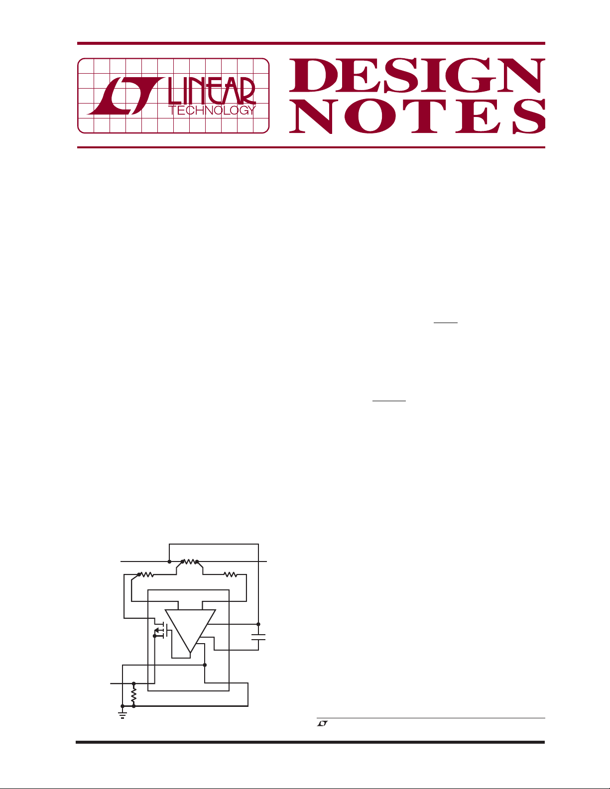
The LTC6102 is easily connected as shown in Figure 1.
The input voltage is developed by the sense resistor, and
the voltage gain of the amplifi er is set by the input and
output resistors. The overall scaling is simply:
=
OUT LOAD SENSE
⎜
⎝
VIR
⎛
•
R
R
OUT
IN
⎞
⎟
–
⎠
The accuracy at small load currents is primarily set by
the input offset voltage V
error I
I
OFFSET
, due to the VOS, is given by:
OFFSET
V
OS
=
R
SENSE
. The current measurement
OS
For a given current offset accuracy requirement, it can
be seen that with a low V
OS
that R
may be reduced
SENSE
accordingly, to sub-milliohms in many applications.
In most applications the circuit gain is selected so that
translates to about 1LSB (least signifi cant bit) in
V
OS
the analog-to-digital (ADC) acquisition system. Dynamic
range is dictated by the maximum signal amplitude that
the ADC can handle and how much power the R
SENSE
resistor is permitted to dissipate.
R
+
V
–
R
IN
–INS
1
–INF
2
–
V
3
V
OUT
OUT
R
4
OUT
SENSE
–
LTC6102
+
R
IN
+IN
+
8
+
V
7
V
REG
6
–
V
5
DN423 F01
Figure 1. Ultraprecise Current Sensing with LTC6102
09/07/423
LOAD
0.1µF
Consider a comparison bet ween two 8-bit sens e amplifi er
solutions, one using a typical amplifi er with V
and one using the LTC6102, where V
= 10μV. The reso-
OS
= 500μV
OS
lution of each is 20mA. The higher offset part requires a
sense resistor of at least 25mΩ, whereas the LTC6102
only requires 500μΩ. At 5A, nearly full-scale current for
this example, the R
power loss is 625mW with the
SENSE
higher offset part, but just 13mW with the LTC6102, a
98% reduction in wasted power.
Print Your Own Sense Resistors
With the ultralow sense resistance capability offered by
the LTC6102, the printed circuit foil itself can be used
as a practical sensing element. A circuit board using 1oz
, LT, LTC and LTM are registered trademarks of Linear Technology Corporation.
All other trademarks are the property of their respective owners.
copper has a nominal sheet resistivity of 500μΩ/square.
The value drops proportionally for thicker foils and rises
for thinner foils. A trace of width W and length L (in any
identical units) has the following resistance:
Rµ
SENSE
≈ 500 Ω •
L
W
The length of the resistor is simply the spacing between
the Kelvin taps along the trace. One ounce copper can
generally carry up to about 100mA/mil of trace width
(or 4A/mm), which constrains the minimum size of the
resistor structure. Another constraint is reproducibility,
so the larger, the bett er. Ultimat ely the thickness toleran ce
and tempco of the copper limit the accuracy a printed
resistor can have.
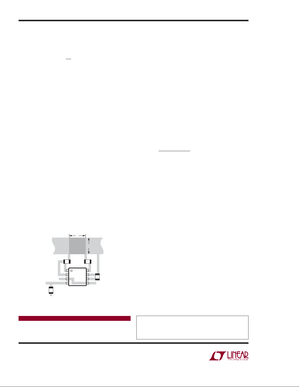
Figure 2 shows a printed structure for the 5A circuit example discussed previously. In this layout, the L/ W factor
is set to 1 (for R
= 500μΩ) and the size is dictated
SENSE
mainly by the accuracy of printed circuit etching.
Using copper for the sense resistance means that the
scaling of the circuit is nearly proportional to absolute
temperature, about +0.4%/°C at room temperature. In
applications where the current is being monitored for
overload protection, the tempco may be convenient, in
that a fi xed protection threshold will automatically correspond to lower current at higher t emperature. For stable
measurements, a software calibration and temperature
correction approach can be used, or the tempco can be
compensated by using a copper-based resistor for R
–
IN
such as a small surface mount inductor with known resistance properties (>10Ω readily available, e.g. Vishay
IMC series).
FROM
SUPPLY
CURRENT CARRYING TRACE
L
R
*
W
SENSE
–
R
IN
+
R
IN
TO LOAD
10A MAX
Design Tips and Details
If you are not printing your own sense resistors, and
need the accuracy of off-the-shelf components, be sure
to specify 4-wire (Kelvin) sense resistors for best results.
Such resistors are designed so that the resistance is well
calibrated between the sensed taps, thus eliminating the
error from solder resistance in the load path.
Accurately measuring microvolt level signals raises the
real possibility of stray thermocouple effects due to dissimilar metallic interconnections. Figure 1 shows the use
of an R
+
that is generally identical to R
IN
–
. The purpose
IN
of this extra resistor is to provide identical metallurgical conditions to both amplifi er inputs for minimizing
thermocouple effects, as well as to minimize DC bias
current imbalance.
–
The R
times of peak measured current I
on R
value is selected to conduct about 500μA at
IN
. The voltage drop
–
is equal to the voltage drop on R
IN
•
IR
IN
–
PEAK SENSE
.≥0 0005
R
PEAK
SENSE
, so:
Gain accuracy of the overall circuit is established mainly
by the quality of the resistors used. This allows the designer to optimize the cost vs performance tradeoff in
each specifi c application.
To minimize copper loss errors in the feedback loop of
the LTC6102, the inverting sense input (–INS) and the
inverting feedback connection (–INF) have been kept
,
separate so that a Kelvin connection to R
–
can be made.
IN
This connection can also be seen in the suggested layout
of Figure 2.
+
Figure 2 shows the V
of R
, whereas Figure 1 shows a tie-in to the supply
SENSE
connections tied to the load side
side. The LTC6102 will work in either confi guration. The
d i f fe re n ce i s t h a t th e F i gu r e 2 co n ne c t i on w il l a ls o in c l ud e
the LTC6102 quiescent supply current (300μA typically)
in the measured load current. Supply voltages from 4V
to 100V are supported.
C
REG
–
OUTPUT
R
OUT
–
V
LTC6102
* 2.5mm × 2.5mm
1oz COPPER
500μΩ
V
DN423 F02
Figure 2. LTC6102 Layout Using Printed Sense Resistance
Data Sheet Download
www.linear.com
Linear Technology Corporation
1630 McCarthy Blvd., Milpitas, CA 95035-7417
(408) 432-1900
●
FAX: (408) 434-0507 ● www.linear.com
Conclusion
The LTC6102 is the industry’s highest precision current
sense amplifi er. The exceptional accuracy allows for dramatic reduc tion in the R
resista nce, thereby improv-
SENSE
ing effi ciency, dynamic range and current handling.
For applications help,
call (408) 432-1900, Ext. 2020
dn423f LT/TP 0907 451K • PRINTED IN THE USA
© LINEAR TECHNOLOGY CORPORATION 2007
 Loading...