


Optimizing the Performance of Very Wideband Direct
Conversion Receivers
Design Note 1027
John Myers, Michiel Kouwenhoven, James Wong, Vladimir Dvorkin
Introduction
Zero-IF receivers are not new; they have been around
for some time and are prominently used in cell phone
handsets. However their use in high performance wireless base stations has had limited success. This is due
primarily to their limited dynamic range and that they
are less well understood. A new wide bandwidth zero-IF
IQ demodulator helps relieve the dynamic range and
bandwidth shor tcomings for main as well as DPD (digital
predistor tion) receiver s, and enables 4G base stat ions to
cost effectively address the ever-increasing bandwidth
needs of mobile access. This article discusses how to
optimize performance by minimizing IM2 nonlinearity
and DC offset that reduce the dynamic range of zeroIF receivers, thus offering a viable alternative to an
otherwise challenging design.
Pushing Ever Wider Bandwidth
Until recently, most base stations needed to only deal
with a 20MHz wide channel bandwidth, typically allocated to various wireless carriers. Associated with this
20MHz channel is a companion 100MHz bandw idth DPD
receiver to measure intermodulation distortion spurs
up to 5th order for effective distortion cancellation.
These requirements can generally be met effectively
w i t h h i g h - I F ( h e t e r o d y n e ) r e c e i v e r s . N o w a d a y s t h o u g h ,
such designs are more challenging, with industry
trends pushing for base stations to support operation
over the entire 60MHz bands. Accomplishing this feat
has signifi cant cost savings implications for the entire
wireless manufacturing, installation and deployment
business model.
To accommo date the three times increase in ba ndwidth,
the DPD receiver b andwidth must increase from 100MHz
to 300MHz. In 75MHz ba nds, the DPD bandwidth grows
to a staggering 375MHz. The design of receivers that
can suppor t this bandwidth is not trivia l. Noise increases
due to the wider bandwi dth, gain fl atness becomes more
diffi cult to achieve, and the required sampling rate of
A/D converters increases dramatically. Furthermore,
the cost of such higher bandwidth components is appreciably higher.
The modest bandwidth of a traditional high-IF receiver
is no longer suffi cient to support the 300MHz or higher
DPD signals with typically ±0.5dB gain fl atness. The
300MHz baseband bandwidth would require choosing an IF frequency of 150MHz at a minimum. It is not
trivial to fi nd an A/D converter capable of a sampling
r a t e u pw a r d of 6 0 0 M s ps t h a t is r e a s on a b l y pr i c e d , e v e n
at 12-bit resolution. One may have to compromise and
resort to a 10-bit converter.
New IQ Demodulator Eases Bandwidth Constraints
The LTC5585 IQ demodulator is designed to support
d i r e c t c o n v e r s i o n , t h u s a l l o w i n g a r e c e i v e r t o d e m o d u l a t e
the aforementioned 300MHz wide RF signal directly to
baseband (see Sidebar: Theory of Operation of a Zero-IF
Receiver). The I and Q outputs are demodulated to a
150MHz wide signal, only half the bandwidth of a highIF receiver. In order to attain a passband gain fl atness
of ±0.5dB, the device’s –3dB corner must extend well
above 500MHz.
The LTC5585 supports this wide bandwidth with a
tunable baseband output stage. The differential I and
Q output ports have a 100Ω pull-up to V
in parallel
CC
with a fi lter capacitance of about 6pF (see Figure 1).
This simple R-C network allows for the formation of
o f f - c hi p lo w p a s s o r b a n d pa s s fi l t e r n et w o r k s t o r em o ve
high level out-of-band blockers and equalization of gain
roll-off the baseband amplifi er chain that follows the
demodulator. With a 100Ω differential output loading
resistance in addition to the external 100Ω pull-up
resistors, the –3dB bandwidth reaches 850MHz.
L, LT, LTC, LTM, Linear Technology and the Linear logo are registered trademarks
of Linear Technology Corporation. All other trademarks are the property of their
respective owners.
03/12/1027
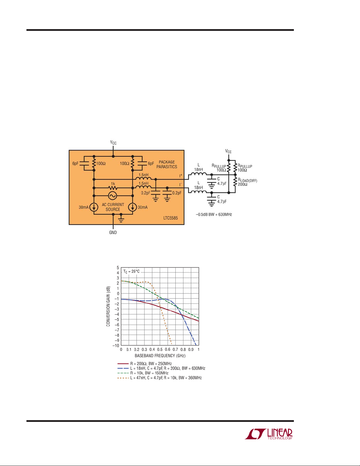
Baseband Bandwidth Extension
A single L-C fi lter section can be used to further extend
the bandwidth of the baseband output. Figure 1 shows
the chip’s baseband equivalent circuit with baseband
bandwidth extension. With 200Ω loading, the –0.5dB
bandwidth can be extended from 250MHz to 630MHz
using a series inductance of 18nH and a shunt capacitance of 4.7pF. Figure 2 shows the variety of output
responses that are possible with different loading. One
r e s p o n s e i s w i t h d i f f e r e n t i a l l o a d i n g r e s i s t a n c e s o f 2 0 0 Ω
and 10kΩ. For 10kΩ loading, the – 0.5dB bandwidth can
be extended from 150MHz to 360MHz using a series
inductance of 47nH and a shunt capacitance of 4.7pF.
Second-Order Intermodulation Distortion Spurs
Matter
In a direct conversion receiver, the second order intermodulation distortion products (IM2) fall directly
in-band at the baseband frequencies. Take, for example,
two equal power RF signals, f1 and f2, spaced 1MHz
apart at 2140MHz and 2141MHz, respectively, while the
LO is spaced 10MHz apart at 2130MHz. The resultant
IM2 spur would fall at f2 – f1, or 1MHz. The LTC5585
has the unique ability to adjust for minimum IM2 spurs
independently on the I and Q channels by using ex ternal
control voltages. Figure 3 shows a t ypical setup for IIP2
measurement and calibr ation. The differen tial baseband
Figure 1. Baseband Output Equivalent Circuit for
Bandwidth Extension with L = 18nH and C = 4.7pF
Figure 2. Conversion Gain vs Baseband
Frequency with Differential Loading
Resistance and L-C Bandwidth Extension
2

outputs are combined using a balun and the 1MHz IM2
difference frequency component is selected with a lowpass fi lter to prevent the strong main tones at 10MHz
and 11MHz from compressing the spectrum analyzer
front end. Without the lowpass fi lter, 20dB to 30dB of
attenuation and long average measurement times are
necessary on the spectrum analyzer to attain a good
measurement. As shown in the output spectrum of
Figure 4, the IM2 component predictably falls in-band
at 1MHz. The plot also shows the IM2 product before
and after adjustment, reducing the spur level by approximately 20dB by adjusting the control voltages on
the IP2I and IP2Q pins. This adjustment reduces the
IM2 spur down to a level of –81.37dBc.
With this IIP2 optimization capability, two possible
strategies of IP2 calibration are possible. One option
is a set-and-forget calibration step performed at the
factory. In this case, a simple trim potentiometer for
each adjustment pin suffi ces, as illustrated in Figure 3.
Alternatively, an automatic, closed loop calibration
algorithm can be implemented in software, allowing
the equipment to be calibrated on a periodic basis.
For DPD receivers that are already monitoring their
transmitters’ output, this is trivial as the transmitters
can easily generate the two test tones. For main receivers, this calibration may involve additional hardware to
loop back the two test tones to the receiver channel. In
any event these can all be performed during an off-line
calibration cycle. Such an approach would take into account the actual operating environmental factors that
may affect base station performance.
Figure 3. Test Setup for IIP2 Calibration with 1MHz
Lowpass Filters to Select the IM2 Component
0
–10
–20
–30
–40
–50
–60
–70
–80
–90
–100
–110
–120
IM2 PRODUCT
BEFORE ADJUST
AFTER
ADJUST
2MHzSTART 0Hz STOP 20MHz
DN1027 F04
Figure 4. Output Spectrum without Lowpass
3

DC Offset Voltage Null Helps to Optimize A/D
Converter Dynamic Range
A similar adjustment capability is also integrated into
the chip to zero out the I and Q’s DC output voltage. DC
offset, a product arising from internal mismatch and
self-mixing of the LO and RF input l eakages, can diminish
the ADC’s dynamic range when the signal chain is DC
coupled throughout. To illustrate, a modest 10mV of
outpu t DC o ffse t vol ta ge, w hen p as se d thro ugh a 2 0dB
gain stage, would result in 100mV of DC offset at the
input of the A/D converter. With 2V
a 12-bit ADC, this amount of DC offset represents 205
LSBs of headroom reduction, or effectively reducing
the ADC’s dynamic range by 0.9dB.
input range of
P-P
Potential Cost Benefi ts of Direct Conversion
Receivers
A zero-IF receiver is particularly compelling due to its
potential cost savings. As mentioned above, the RF
signal demodulates to a low frequency baseband. At
lower frequencies, the design of the fi lter becomes easier.
F ur t h e rm or e , z er o -I F de mo d ul a ti o n p ro du ce s no i ma ge
at the baseb and, thus eliminating the need for a relati vely
expensive SAW fi lter. Perhaps most attractive is that
the ADC sampling rate can be signifi cantly reduced.
In the example above, the 150MHz I and Q baseband
bandwidth can be effectively addressed with a dual
310Msps ADC such as LTC2258-14, without resorting
to a much more expensive higher sampling rate ADC.
To minimize the leakage between the LO and RF inputs,
care should be taken to isolate these two signals. In the
PCB layout, separate these two signal traces from one
another to prevent cross-coupling. The LO signal, even
if there is measurable leakage to the RF port, will selfmix to form a DC offset term at the output. Fortunately
the LO level is usually constant, so the DC offset voltage is also constant and can be easily canceled by the
adjustment. More problematic is the RF input, which
can vary over wide signal levels. Any signal leakage to
the LO input would self-mix and produce a dynamic
DC offset voltage as the signal varies. This will distort
the demodulated signal. So keeping the leakage small
helps reduce the DC offset to a minimum.
Conclusion
As the bandwidth and performance of wireless receivers increase, a new wideband quadrature demodulator
offers an alternative approach that helps to address
architectural shortcomings and raises receiver performance while reducing systems costs.
4

SIDEBAR
THEORY OF OPERATION OF IQ DEMODULATION
IQ Demodulation
The operation of an IQ demodulator can be explained by
representing its RF input signal S
(t) as a combination
RF
of two double sideband modulated quadrature carriers:
(t) = SI(t) + SQ(t) = l(t)cosωRFt – Q(t)sinωRFt (1)
S
RF
As illustrated in Figure A, the in-phase component I(t)
and quadrature component Q(t) are baseband signals
that can be viewed as inputs to an ideal IQ modulator
generating S
RF
(t).
An IQ demodulator achieves perfect reconstruction of
I(t) and Q(t) by exploiting the quadrature phase relation between S
(t) and SQ(t). The frequency-domain
I
representation of a –90° phase-shift corresponds to
multiplication by the Hilbert transform:
H(jω) = jsgn(ω) (2)
It converts a spectrum with even symmetry around
ω =0 to a spectrum with odd symmetry and vice
versa. The spectra of S
different symmetr y; S
(t) and SQ(t) therefore exhibit
I
(t) has even symmetry, SQ(t) has
I
odd symmetry. Downconversion of the even RF input
component S
I(t), while S
(t) with the even LO (cosine) retrieves
I
(t) with the odd LO (sine) retrieves Q(t).
Q
Cross-combinations of even and odd yield zero.
An error ϕ on the quadrature relation between the LO
outputs caus es crosstalk bet ween the I- and Q-channels.
Using the I-phase channel as reference, an even component is introduced in the Q-channel LO:
sin(ω
t + ϕ) = sin(ωRFt)cosϕ + cos(ωRFt)sin ϕ (3)
RF
resulting in a contribution of I(t) to the Q-channel
output Q
Q
OUT
(t):
OUT
(t) = Q(t)cosϕ + l(t)sinϕ (4)
Image Cancellation Receiver
Another IQ demodulator application is an image rejection/cancellation receiver with non-zero IF frequency,
as shown in Figure B.
Figure A. Concept of IQ Modulation and IQ Demodulation
Figure B. Operation of the Hartley Image Rejection Receiver
5

The I-channel preserves the symmetry in the RF input
signal, while the Q-channel converts even components
to odd and vice versa. The extra 90° phase shifter restores the original symmetry in the Q-channel, but with
opposite sign for the signals S
(t) is ahead of the LO since its center frequency is
of S
2
higher, while the phase of S
(t) and S2(t); the phase
1
(t) lags behind. Addition to
1
the I-channel reconstructs the downconverted signal
(t); subtraction reconstructs S1(t).
S
2
The image rejection (IR) is degraded in the presence of
a quadrature pha se error ϕ or gain mismatch α between
I- and Q-channels. The ph ase error introduces crosstalk
between the channels, while gain mismatch results in
imperfect cancellation by the adder:
2
IR = 10log
⎛
⎜
⎝
1+ α
1+ α
+ 2αcosϕ
2
− 2αcosϕ
⎞
⎟
⎠
(5)
Figure C depicts the result for different gain and phase
error combinations. Small gain errors have a larger
impact than small phase errors.
Data Sheet Download
www.linear.com
Figure C. Image Rejection vs Phase Error for Different I/Q Gain Mismatch
For applications help,
call (408) 432-1900, Ext. 2482
Linear Technology Corporation
1630 McCarthy Blvd., Milpitas, CA 95035-7417
(408) 432-1900
●
FAX: (408) 434-0507 ● www.linear.com
dn1027f LT/TP 0312 305K • PRINTED IN THE USA
© LINEAR TECHNOLOGY CORPORATION 2012
 Loading...