

Linear Technology LTC489, LTC488 Datasheet
LTC488/LTC489
Quad RS485 Line Receiver
EATU
F
■
Low Power: ICC = 7mA Typ
■
Designed for RS485 or RS422 Applications
■
Single 5V Supply
■
–7V to 12V Bus Common Mode Range Permits ±7V
RE
S
Ground Difference Between Devices on the Bus
■
60mV Typical Input Hysteresis
■
Receiver Maintains High Impedance in Three-State or
with the Power Off
■
28ns Typical Receiver Propagation Delay
■
Pin Compatible with the SN75173 (LTC488)
■
Pin Compatible with the SN75175 (LTC489)
U
O
PPLICATI
A
■
Low Power RS485/RS422 Receivers
■
Level Translator
S
DUESCRIPTIO
The LTC®488 and LTC489 are low power differential bus/
line receivers designed for multipoint data transmission
standard RS485 applications with extended common mode
range (12V to –7V). They also meet the requirements of
RS422.
The CMOS design offers significant power savings over its
bipolar counterpart without sacrificing ruggedness against
overload or ESD damage.
The receiver features three-state outputs, with the receiver
output maintaining high impedance over the entire common mode range.
The receiver has a fail-safe feature which guarantees a
high output state when the inputs are left open.
Both AC and DC specifications are guaranteed 4.75V to
5.25V supply voltage range.
, LTC and LT are registered trademarks of Linear Technology Corporation.
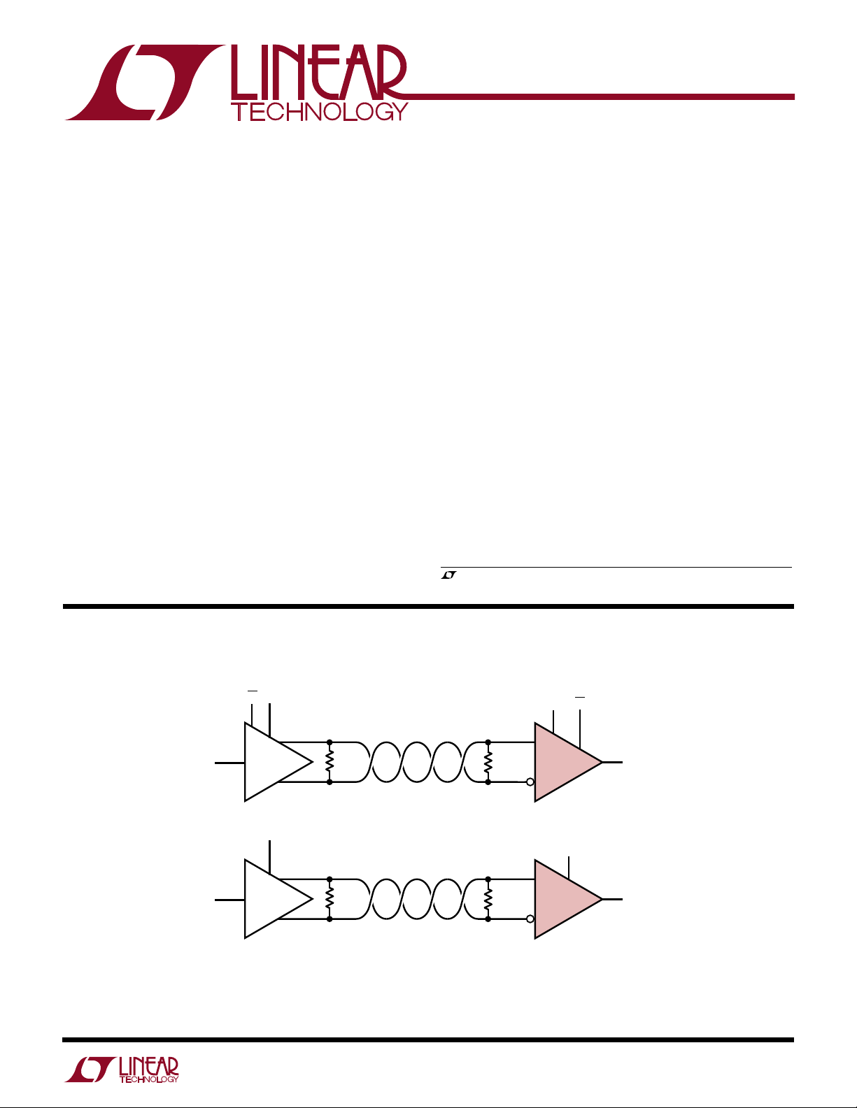
A
U
O
PPLICATITYPICAL
EN
EN
2
DI
DI
DRIVER
1/4 LTC486
EN12
DRIVER
1/4 LTC487
120Ω
4000 FT 24 GAUGE TWISTED PAIR
120Ω
4000 FT 24 GAUGE TWISTED PAIR
120Ω
120Ω
1
2
1
EN
4
RECEIVER
1/4 LTC488
EN12
4
RECEIVER
1/4 LTC489
EN
12
3
RO
3
RO
LTC488/9 TA01
1
LTC488/LTC489
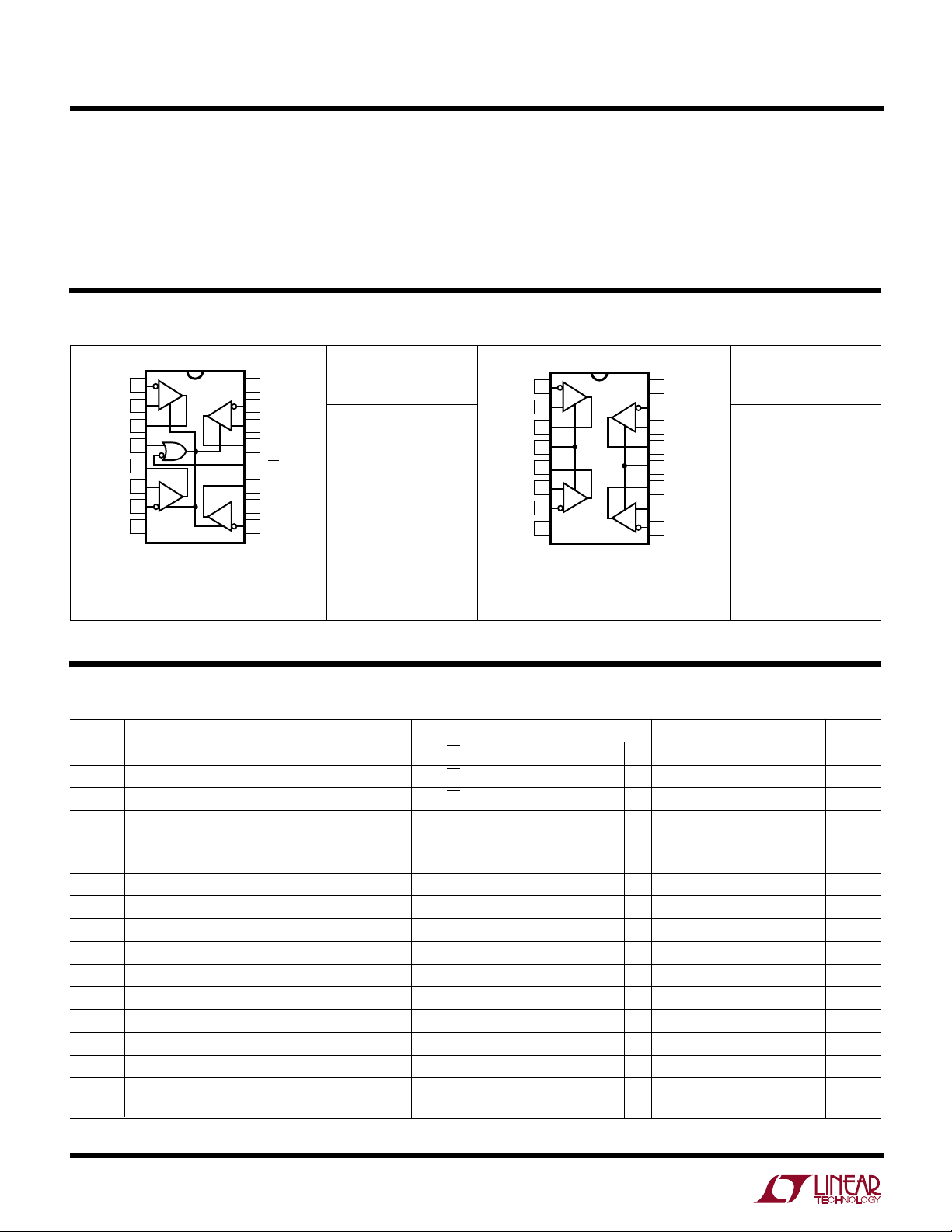
A
W
O
LUTEXI T
S
A
WUW
ARB
U
G
I
(Note 1)
S
Supply Voltage (VCC) .............................................. 12V
Control Input Currents ........................ – 25mA to 25mA
Control Input Voltages ................ –0.5V to (VCC + 0.5V)
Receiver Input Voltages ........................................ ±14V
Receiver Output Voltages ........... – 0.5V to (VCC + 0.5V)
WU
/
PACKAGE
1
B1
2
A1
3
RO1
4
EN
5
RO2
6
A2
7
B2
8
GND
N PACKAGE
16-LEAD PLASTIC DIP
T
= 150°C, θJA = 70°C/W (N PKG)
JMAX
= 150°C, θJA = 90°C/W (S PKG)
T
JMAX
O
TOP VIEW
R
R
16-LEAD PLASTIC SOL
RDER I FOR ATIO
ORDER PART
V
16
15
R
14
13
12
11
10
R
9
S PACKAGE
CC
B4
A4
RO4
EN
RO3
A3
B3
NUMBER
LTC488CN
LTC488CS
LTC488IN
LTC488IS
Operating Temperature Range
LTC488C/LTC489C ................................. 0°C to 70°C
LTC488I/LTC489I .............................. –40°C to 85°C
Storage Temperature Range ................ – 65°C to 150°C
Lead Temperature (Soldering, 10 sec)................. 300°C
U
TOP VIEW
1
B1
A1
RO1
EN12
RO2
A2
B2
GND
N PACKAGE
16-LEAD PLASTIC DIP
R
2
3
4
5
6
R
7
8
T
= 150°C, θJA = 70°C/W (N PKG)
JMAX
= 150°C, θJA = 90°C/W (S PKG)
T
JMAX
V
16
CC
B4
15
R
R
16-LEAD PLASTIC SOL
14
13
12
11
10
9
S PACKAGE
A4
RO4
EN34
RO3
A3
B3
ORDER PART
NUMBER
LTC489CN
LTC489CS
LTC489IN
LTC489IS
Consult factory for Military grade parts.
LECTRICAL C CHARA TERIST
E
SYMBOL PARAMETER CONDITIONS MIN TYP MAX UNITS
V
INH
V
INL
I
IN1
I
IN2
V
TH
∆V
TH
V
OH
V
OL
I
OZR
I
CC
RINReceiver Input Resistance –7V ≤ VCM ≤ 12V, VCC = 0V ● 12 kΩ
I
OSR
t
PLH
t
PHL
t
SKD
Input High Voltage EN, EN, EN12, EN34 ● 2.0 V
Input Low Voltage EN, EN, EN12, EN34 ● 0.8 V
Input Current EN, EN, EN12, EN34 ● ±2 µA
Input Current (A, B) VCC = 0V or 5.25V, VIN = 12V ● 1.0 mA
Differential Input Threshold Voltage for Receiver –7V ≤ VCM ≤ 12V ● – 0.2 0.2 V
Receiver Input Hysteresis VCM = 0V 60 mV
Receiver Output High Voltage IO = – 4mA, VID = 0.2V ● 3.5 V
Receiver Output Low Voltage IO = 4mA, VID = – 0.2V ● 0.4 V
Three-State Output Current at Receiver VCC = Max 0.4V ≤ VO ≤ 2.4V ● ±1 µA
Supply Current No Load, Digital Pins = GND or V
Receiver Short-Circuit Current 0V ≤ VO ≤ V
Receiver Input to Output CL = 15pF (Figures 1, 3) ● 12 28 55 ns
Receiver Input to Output CL = 15pF (Figures 1, 3) ● 12 28 55 ns
| t
– t
PLH
Differential Receiver Skew
|C
PHL
VCC = 5V (Notes 2, 3), unless otherwise noted.
ICSCD
= 0V or 5.25V, VIN = – 7V ● – 0.8 mA
V
CC
● 710 mA
CC
CC
= 15pF (Figures 1, 3) 4 ns
L
● 785mA
2
LTC488/LTC489
OUTPUT VOLTAGE (V)
0
0
OUTPUT CURRENT (mA)
16
1.0
488 G04
8
0.5 1.5
24
32
2.0
4
12
20
28
36
LECTRICAL C CHARA TERIST
E
VCC = 5V ± 5% (Notes 2, 3), unless otherwise noted.
ICSCD
SYMBOL PARAMETER CONDITIONS MIN TYP MAX UNITS
t
ZL
t
ZH
t
LZ
t
HZ
The ● denotes specifications that apply over the operating temperature
range.
Note 1: Absolute Maximum Ratings are those beyond which the safety of
the device may be impaired.
Receiver Enable to Output Low CL = 15pF (Figures 2, 4) S1 Closed ● 30 60 ns
Receiver Enable to Output High CL = 15pF (Figures 2, 4) S2 Closed ● 30 60 ns
Receiver Disable from Low CL = 15pF (Figures 2, 4) S1 Closed ● 30 60 ns
Receiver Disable from High CL = 15pF (Figures 2, 4) S2 Closed ● 30 60 ns
Note 2: All currents into device pins are positive; all currents out of device
pins are negative. All voltages are referenced to device ground unless
otherwise specified.
Note 3: All typicals are given for V
= 5V and TA = 25°C.
CC
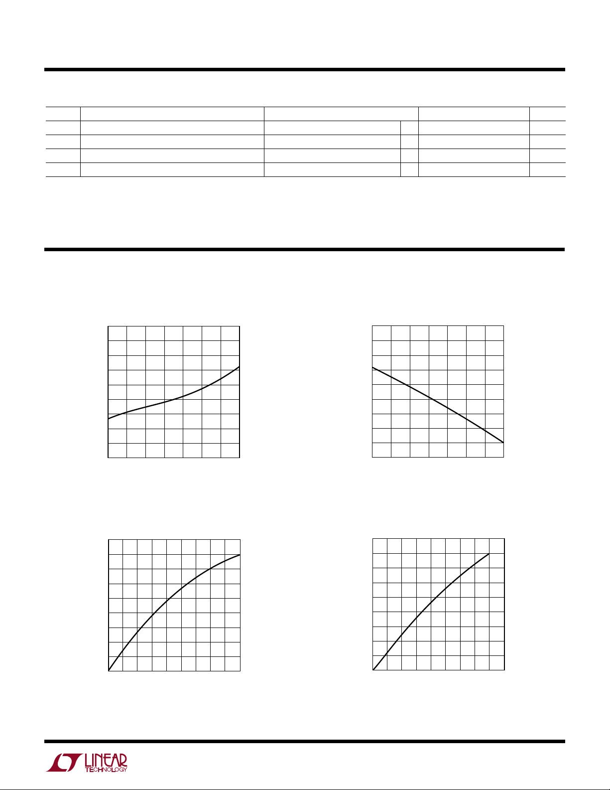
UW
LPER
F
O
R
ATYPICA
Receiver Output Low Voltage vs
Temperature at I = 8mA
0.9
0.8
0.7
0.6
0.5
0.4
0.3
OUTPUT VOLTAGE (V)
0.2
0.1
0
–25 125
–50
0
TEMPERATURE (°C)
50
25
CCHARA TERIST
E
C
75 100
488 G01
ICS
4.8
4.6
4.4
4.2
4.0
3.8
3.6
OUTPUT VOLTAGE (V)
3.4
3.2
3.0
Receiver Output High Voltage vs
Temperature at I = 8mA
–25 125
–50
0
25
TEMPERATURE (°C)
50
75 100
488 G02
Receiver Output High Voltage vs
Output Current at TA = 25°C
–18
–16
–14
–12
–10
–8
–6
OUTPUT CURRENT (mA)
–4
–2
0
5
43
OUTPUT VOLTAGE (V)
Receiver Output Low Voltage vs
Output Current at TA = 25°C
2
488 G03
3
LTC488/LTC489
TEMPERATURE (°C)
–50
5.4
SUPPLY CURRENT (mA)
6.2
50
488 G07
5.8
–25 125
6.6
7.0
0
25
75 100
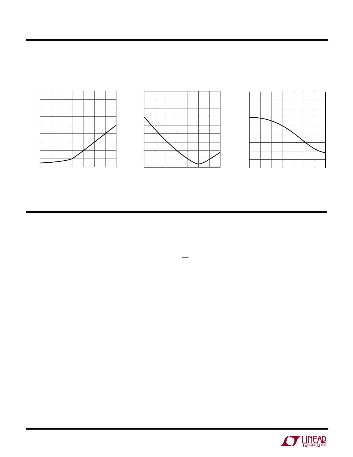
LPER
F
O
R
ATYPICA
UW
CCHARA TERIST
E
C
ICS
TTL Input Threshold vs
Temperature
1.63
1.61
1.59
1.57
INPUT THRESHOLD VOLTAGE (V)
1.55
–50
0
–25 125
25
TEMPERATURE (°C)
U
75 100
50
488 G05
UU
Receiver |t
Temperature
5
4
3
TIME (ns)
2
1
–50
PLH
0
–25 125
TEMPERATURE (°C)
PI FU CTIO S
B 1 (Pin 1) Receiver 1 Input.
A1 (Pin 2) Receiver 1 Input.
RO1 (Pin 3) Receiver 1 Output. If the receiver output is
enabled, then if A > B by 200mV, RO1 will be high. If
A < B by 200mV, then RO1 will be low.
EN (Pin 4) (LTC488) Receiver Output Enabled. See
Function Table for details.
EN12 (Pin 4) (LTC489) Receiver 1, Receiver 2 Output
Enabled. See Function Table for details.
RO2 (Pin 5) Receiver 2 Output. Refer to RO1.
A2 (Pin 6) Receiver 2 Input.
B2 (Pin 7) Receiver 2 Input.
GND (Pin 8) Ground Connection.
– t
| vs
PHL
25
75 100
50
488 G06
Supply Current vs Temperature
B3 (Pin 9) Receiver 3 Input.
A3 (Pin 10) Receiver 3 Input.
RO3 (Pin 11) Receiver 3 Output. Refer to RO1.
EN (Pin 12)(LTC488) Receiver Output Disabled. See
Function Table for details.
EN34 (Pin 12)(LTC489) Receiver 3, Receiver 4 output
enabled. See Function Table for details.
RO4 (Pin 13) Receiver 4 Output. Refer to RO1.
A4 (Pin 14) Receiver 4 Input.
B4 (Pin 15) Receiver 4 Input.
V
(Pin 16) Positive Supply; 4.75V ≤ VCC ≤ 5.25V.
CC
4
 Loading...