

Linear Technology LTC487 Datasheet
LTC487
Quad Low Power
RS485 Driver
EATU
F
■
Very Low Power: ICC = 110µA Typ
■
Designed for RS485 or RS422 Applications
■
Single 5V Supply
■
–7V to 12V Bus Common-Mode Range Permits
RE
S
±7V GND Difference Between Devices on the Bus
■
Thermal Shutdown Protection
■
Power-Up/Down Glitch-Free Driver Outputs Permit
Live Insertion/Removal of Package
■
Driver Maintains High Impedance in Three-State or
with the Power Off
■
28ns Typical Driver Propagation Delays with
5ns Skew
■
Pin Compatible with the SN75174, DS96174,
µA96174, and DS96F174
U
O
PPLICATI
A
■
Low Power RS485/RS422 Drivers
■
Level Translator
S
DUESCRIPTIO
The LTC487® is a low power differential bus/line driver
designed for multipoint data transmission standard RS485
applications with extended common-mode range (– 7V to
12V). It also meets RS422 requirements.
The CMOS design offers significant power savings over its
bipolar counterpart without sacrificing ruggedness against
overload or ESD damage.
The driver features three-state outputs, with the driver
outputs maintaining high impedance over the entire common-mode range. Excessive power dissipation caused by
bus contention or faults is prevented by a thermal shutdown circuit which forces the driver outputs into a high
impedance state.
Both AC and DC specifications are guaranteed from 0°C to
70°C (Commercial), –40°C to 85°C (Industrial) and over
the 4.75V to 5.25V supply voltage range.
DI
EN 12
1
DRIVER
1/4 LTC487
and LTC are registered trademarks and LT is a trademark of Linear Technology Corporation.
U
O
A
PPLICATITYPICAL
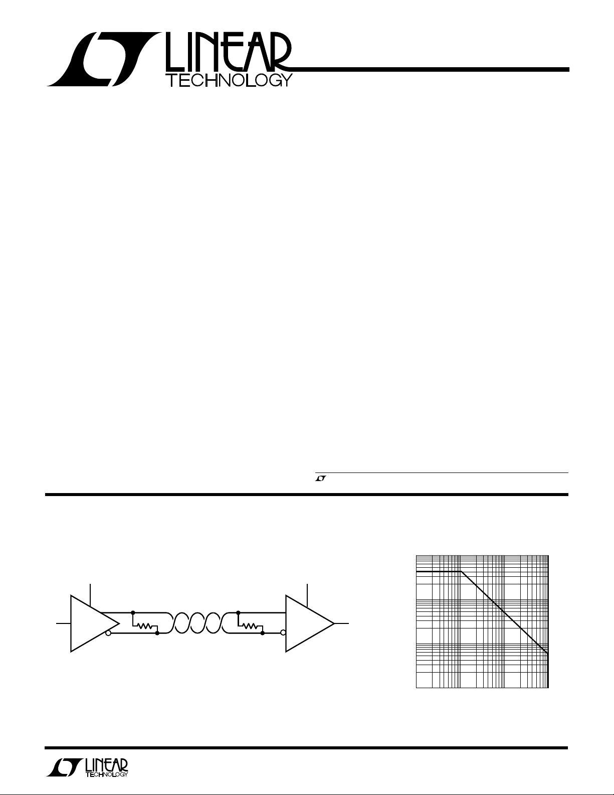
RS485 Cable Length Specification*
10k
EN 12
4
2
120Ω 120Ω
3
4000 FT BELDEN 9841
2
1
4
RECEIVER
1/4 LTC489
3
LTC487 • TA01
RO
1k
100
CABLE LENGTH (FT)
10
10k
* APPLIES FOR 24 GAUGE, POLYETHYLENE
DIELECTRIC TWISTED PAIR
100k 1M 10M
DATA RATE (bps)
2.5M
LTC487 • TA09
1
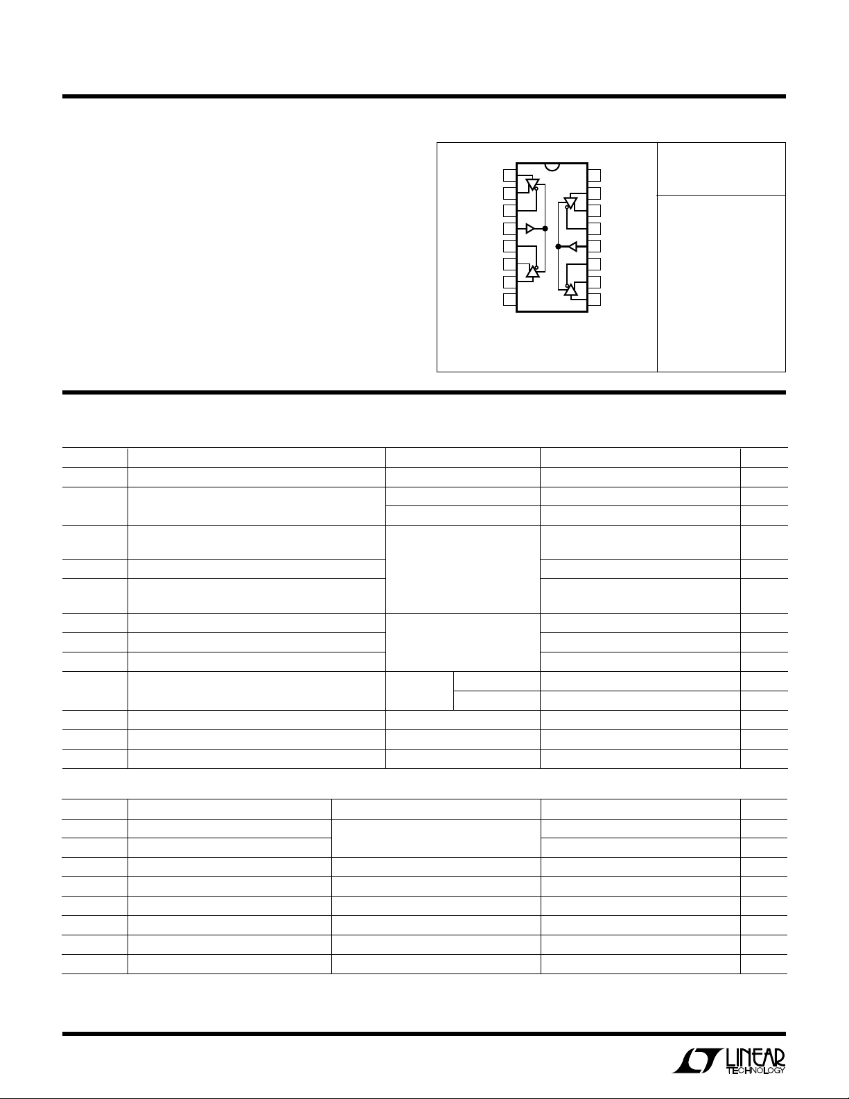
LTC487
WU
U
PACKAGE
/
O
RDER I FOR ATIO
W
O
A
(Note 1)
LUTEXI T
S
Supply Voltage (VCC) ............................................... 12V
Control Input Voltages .................... –0.5V to VCC + 0.5V
Driver Input Voltages ...................... –0.5V to VCC + 0.5V
Driver Output Voltages .......................................... ±14V
Control Input Currents ........................................ ±25mA
Driver Input Currents .......................................... ±25mA
Operating Temperature Range
Commercial ............................................ 0°C to 70°C
Industrial ........................................... – 40°C to 85°C
Storage Temperature Range ................. –65°C to 150°C
Lead Temperature (Soldering, 10 sec.).................300°C
LECTRICAL C CHARA TERIST
E
VCC = 5V ±5%, 0°C ≤ TA ≤ 70°C (Commercial), –40°C ≤ TA ≤ 85°C (Industrial) (Note 2, 3)
SYMBOL PARAMETER CONDITIONS MIN TYP MAX UNITS
V
OD1
V
OD2
V
OD
V
OC
V
Change in Magnitude of Driver Common-Mode 0.2 V
OC
V
IH
V
IL
I
IN1
I
CC
I
OSD1
I
OSD2
I
OZ
Differential Driver Output Voltage (Unloaded) IO = 0 5 V
Differential Driver Output Voltage (With Load) R = 50Ω; (RS422) 2 V
Change in Magnitude of Driver Differential R = 27Ω or R = 50Ω 0.2 V
Output Voltage for Complementary Output States (Figure 3)
Driver Common-Mode Output Voltage 3V
Output Voltage for Complementary Output States
Input High Voltage DI, EN12, EN34 2.0 V
Input Low Voltage 0.8 V
Input Current ±2 µA
Supply Current No Load Output Enabled 110 200 µA
Driver Short-Circuit Current, V
Driver Short-Circuit Current, V
High Impedance State Output Current VO = –7V to 12V ±10 ±200 µA
A
WUW
OUT
OUT
U
ARB
G
I
S
TOP VIEW
1
DI1
2
DO1A
3
DO1B
4
EN12
5
DO2B
6
DO2A
DI2
7
GND
8
N PACKAGE
16-LEAD PLASTIC DIP
T
= 125°C, θJA = 70°C/W (N)
JMAX
= 150°C, θJA = 95°C/W (S)
T
JMAX
Consult factory for Military grade parts.
16
V
CC
15
DI4
14
DO4A
13
DO4B
12
EN34
11
DO3B
DO3A
10
DI3
9
S PACKAGE
16-LEAD PLASTIC SOL
ORDER PART
NUMBER
LTC487CN
LTC487CS
LTC487IN
LTC487IS
ICSCD
R = 27Ω; (RS485) (Figure 3) 1.5 5 V
Output Disabled 110 200 µA
= High VO = –7V 100 250 mA
= Low VO = 12V 100 250 mA
U
S
WI
SYMBOL PARAMETER CONDITIONS MIN TYP MAX UNITS
t
PLH
t
PHL
t
SKEW
t
r, tf
t
ZH
t
ZL
t
LZ
t
HZ
Note 1: Absolute maximum ratings are those beyond which the safety of
the device cannot be guaranteed.
Note 2: All currents into device pins are positive; all currents out of device
I
TCH
GC CHARA TERIST
Driver Input to Output R
Driver Input to Output
Driver Output to Output 515ns
Driver Rise or Fall Time 5 20 25 ns
Driver Enable to Output High CL = 100pF (Figures 2, 5) S2 Closed 35 70 ns
Driver Enable to Output Low CL = 100pF (Figures 2, 5) S1 Closed 35 70 ns
Driver Disable Time from Low CL = 15pF (Figures 2, 5) S1 Closed 35 70 ns
Driver Disable Time from High CL = 15pF (Figures 2, 5) S2 Closed 35 70 ns
VCC = 5V ±5%, 0°C ≤ TA ≤ 70°C (Note 2, 3)
ICS
= 54Ω, CL1 = CL2 = 100pF 10 30 50 ns
DIFF
(Figures 1, 4)
pins are negative. All voltages are referenced to device GND unless
otherwise specified.
Note 3: All typicals are given for V
10 30 50 ns
= 5V and Temperature = 25°C.
CC
2
UW
TEMPERATURE (°C )
–50
SUPPLY CURRENT (µA)
90
100
110
120
130
0 50 100
LTC487 • TPC06
OUTPUT VOLTAGE (V)
0
OUTPUT CURRENT (mA)
0
20
40
60
80
1234
LTC487 • TPC03
TA = 25°C
Y
PICA
LPER
F
O
R
AT
CCHARA TERIST
E
C
ICS
Driver Output High Voltage Driver Differential Output Voltage Driver Output Low Voltage
vs Output Current vs Output Current vs Output Current
LTC487
–96
–72
– 4 8
OUTPUT CURRENT (mA)
–24
0
0
1234
OUTPUT VOLTAGE (V)
TA = 25°C
LTC487 • TPC01
64
48
32
OUTPUT CURRENT (mA)
16
0
0
1234
OUTPUT VOLTAGE (V)
TA = 25°C
LTC487• TPC02
TTL Input Threshold vs Temperature Driver Skew vs Temperature Supply Current vs Temperature
1.63
1.61
1.59
5.0
4.0
3.0
TIME (ns)
1.57
INPUT THRESHOLD VOLTAGE (V)
1.55
–50
0 50 100
TEMPERATURE (°C )
LTC487 • TPC04
2.0
1.0
–50
0 50 100
TEMPERATURE (°C )
Driver Differential Output
Voltage vs Temperature
2.3
2.1
1.9
1.7
DIFFERENTIAL VOLTAGE (V)
1.5
–50
0 50 100
TEMPERATURE (°C )
LTC487 • TPC05
RO = 54Ω
LTC487 • TPC07
3
 Loading...