

Linear Technology LTC485IN8, LTC485CS8, LTC485CN8, LTC485, LTC485MJ8 Datasheet
...
LTC485
Low Power RS485
Interface Transceiver
EATU
F
■
Low Power: ICC = 300µA Typ
■
Designed for RS485 Interface Applications
■
Single 5V supply
■
–7V to 12V Bus Common-Mode Range Permits
RE
S
±7V Ground Difference Between Devices on the Bus
■
Thermal Shutdown Protection
■
Power-Up/Down Glitch-Free Driver Outputs
Permit Live Insertion or Removal of Transceiver
■
Driver Maintains High Impedance in Three-State
or with the Power Off
■
Combined Impedance of a Driver Output and
Receiver Allows Up to 32 Transceivers on the Bus
■
70mV Typical Input Hysteresis
■
30ns Typical Driver Propagation Delays
with 5ns Skew
■
Pin Compatible with the SN75176A, DS75176A
and µA96176
U
O
PPLICATI
A
S
DUESCRIPTIO
The LTC485 is a low power differential bus/line transceiver
designed for multipoint data transmission standard RS485
applications with extended common-mode range (12V to
–7V). It also meets the requirements of RS422.
The CMOS design offers significant power savings over its
bipolar counterpart without sacrificing ruggedness against
overload of ESD damage.
The driver and receiver feature three-state outputs, with
the driver outputs maintaining high impedance over the
entire common-mode range. Excessive power dissipation
caused by bus contention or faults is prevented by a
thermal shutdown circuit which forces the driver outputs
into a high impedance state.
The receiver has a fail-safe feature which guarantees a
high output state when the inputs are left open.
The LTC485 is fully specified over the commercial and
extended industrial temperature range.
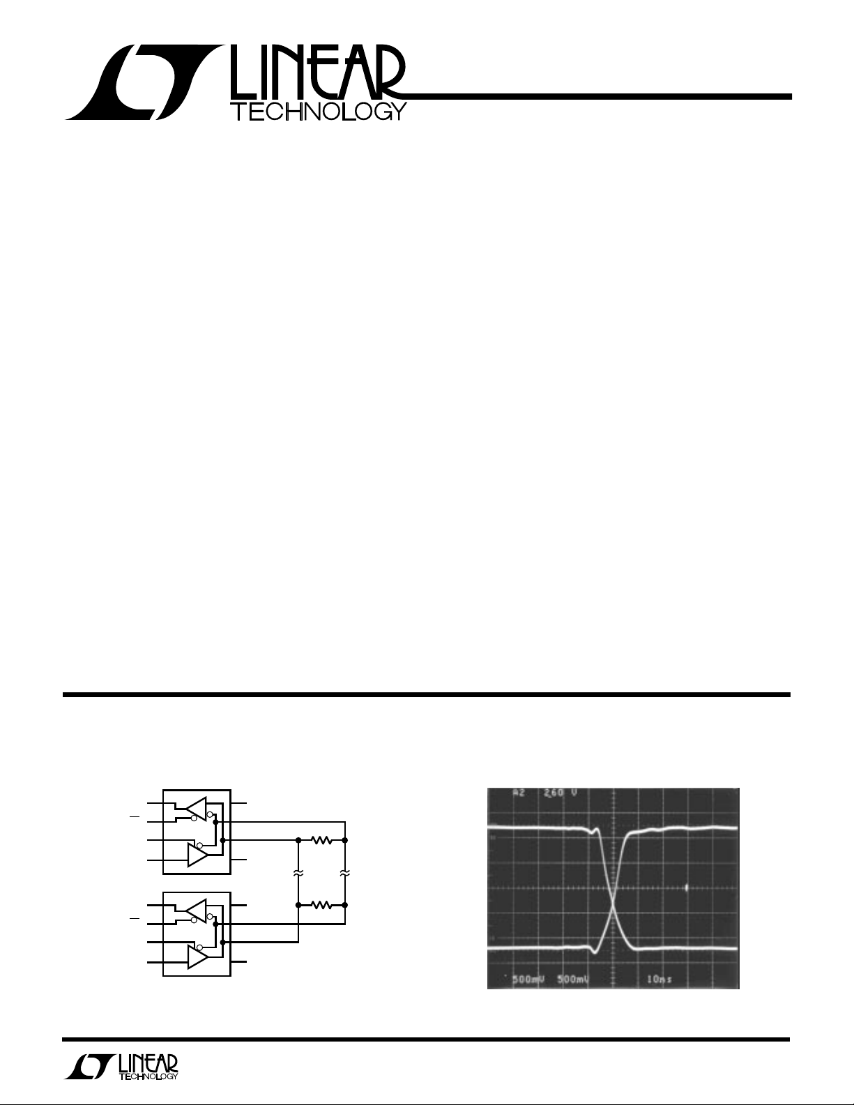
■
Low Power RS485/RS422 Transceiver
■
Level Translator
O
A
PPLICATITYPICAL
RO1
RE1
DE1
DI1
RO2
RE2
DE2
DI2
R
D
R
D
V
CC1
GND1
V
CC2
GND2
U
Rt
Rt
LTC485 • TA01
Driver Outputs
A
B
LTC485 • TA02
1
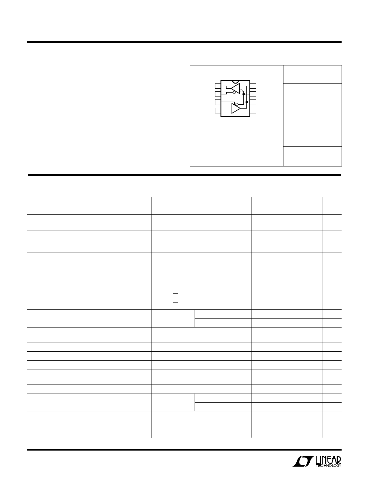
LTC485
A
W
O
LUTEXI T
S
A
WUW
ARB
U
G
I
S
PACKAGE
/
O
RDER I FOR ATIO
WU
(Note 1)
Supply Voltage ....................................................... 12V
Control Input Voltages ................... – 0.5V to VCC + 0.5V
Driver Input Voltage....................... – 0.5V to VCC + 0.5V
Driver Output Voltage ........................................... ±14V
RO
RE
DE
Receiver Input Voltage.......................................... ±14V
Receiver Output Voltages .............. –0.5V to VCC + 0.5V
Operating Temperature Range
J8 PACKAGE
8-LEAD CERAMIC DIP
LTC485I...................................... –40°C ≤ TA ≤ 85°C
LTC485C.......................................... 0°C ≤ TA ≤ 70°C
LTC485M.................................. – 55°C ≤ TA ≤ 125°C
Lead Temperature (Soldering, 10 sec)................. 300°C
V
LECTRICAL C CHARA TERIST
E
SYMBOL PARAMETER CONDITIONS MIN TYP MAX UNITS
V
OD1
V
OD2
∆V
OD
V
OC
∆V
OC
V
IH
V
IL
I
IN1
I
IN2
V
TH
∆V
TH
V
OH
V
OL
I
OZR
R
IN
I
CC
I
OSD1
I
OSD2
I
OSR
Differential Driver Output Voltage (Unloaded) IO = 0 ● 5V
Differential Driver Output Voltage (with Load) R = 50Ω (RS422) ● 2V
Change in Magnitude of Driver R = 27Ω or R = 50Ω, Figure 1 ● 0.2 V
DifferentialOutput Voltage for
Complementary States
Driver Common-Mode Output Voltage R = 27Ω or R = 50Ω, Figure 1 ● 3V
Change in Magnitude of Driver R = 27Ω or R = 50Ω, Figure 1 ● 0.2 V
Common-Mode Output Voltage
for Complementary States
Input High Voltage DE, DI, RE ● 2V
Input Low Voltage DE, DI, RE ● 0.8 V
Input Current DE, DI, RE ● ±2 µA
Input Current (A, B) DE = 0, VCC = 0V VIN = 12V ● ±1mA
Differential Input Threshold Voltage –7V ≤ VCM ≤ 12V ● –0.2 0.2 V
for Receiver
Receiver Input Hysteresis VCM = 0V ● 70 mV
Receiver Output High Voltage IO = –4mA, VID = 200mV ● 3.5 V
Receiver Outpu Low Voltage IO = 4mA, VID = –200mV ● 0.4 V
Three-State (High Impedance) Output VCC = Max, 0.4V ≤ VO ≤ 2.4V ● ±1 µA
Current at Receiver
Receiver Input Resistance –7V ≤ VCM ≤ 12V ● 12 kΩ
Supply Current No Load, Pins 2, Outputs Enabled ● 500 900 µA
Driver Short-Circuit Current, V
Driver Short-Circuit Current, V
Receiver Short-Circuit Current 0V ≤ VO ≤ V
= HIGH VO = –7V ● 35 100 250 mA
OUT
= LOW VO = 10V ● 35 100 250 mA
OUT
ICS
= 5V ±5%, unless otherwise noted. (Notes 2 and 3)
CC
R = 27Ω (RS485), Figure 1
or 5.25V
3, 4 = 0V or 5V
CC
T
T
= –7V ● –0.8 mA
V
IN
Outputs Disabled
TOP VIEW
1
2
3
DI
T
JMAX
JMAX
JMAX
D
4
S8 PACKAGE
8-LEAD PLASTIC SOIC
= 155°C, θ
= 100°C, θ
= 100°C, θ
V
8
R
8-LEAD PLASTIC DIP
= 100°C/ W (J)
JA
= 130°C/ W (N)
JA
= 170°C/ W (S)
JA
CC
B
7
A
6
GND
5
N8 PACKAGE
● 1.5 5 V
● 300 500 µA
● 785mA
ORDER PART
NUMBER
LTC485CJ8
LTC485CN8
LTC485CS8
LTC485IN8
LTC485IS8
LTC485MJ8
S8 PART MARKING
485
485I
U
2
LTC485
U
SWITCHI G CHARACTERISTICS
SYMBOL PARAMETER CONDITIONS MIN TYP MAX UNITS
t
PLH
t
PHL
t
SKEW
t
, t
r
f
tZHDriver Enable to Output High CL = 100pF (Figures 4 and 6) S2 Closed ● 40 70 ns
t
ZL
t
LZ
t
HZ
t
PLH
t
PHL
t
SKD
t
ZL
t
ZH
t
LZ
t
HZ
Driver Input to Output R
Driver Input to Output
Driver Output to Output ● 510ns
Driver Rise or Fall Time ● 31525ns
Driver Enable to Output Low CL = 100pF (Figures 4 and 6) S1 Closed ● 40 70 ns
Driver Disable Time from Low CL = 15pF (Figures 4 and 6) S1 Closed ● 40 70 ns
Driver Disable Time from High CL = 15pF (Figures 4 and 6) S2 Closed ● 40 70 ns
Receiver Input to Output R
t
– t
PLH
Differential Receiver Skew ● 13 ns
PHL
Receiver Enable to Output Low CRL = 15pF (Figures 2 and 8) S1 Closed ● 20 50 ns
Receiver Enable to Output High CRL = 15pF (Figures 2 and 8) S2 Closed ● 20 50 ns
Receiver Disable from Low CRL = 15pF (Figures 2 and 8) S1 Closed ● 20 50 ns
Receiver Disable from High CRL = 15pF (Figures 2 and 8) S2 Closed ● 20 50 ns
VCC = 5V ±5%, unless otherwise noted. (Notes 2 and 3)
= 54Ω, CL1 = CL2 = 100pF, ● 10 30 50 ns
DIFF
(Figures 3 and 5)
= 54Ω, CL1 = CL2 = 100pF, ● 30 90 200 ns
DIFF
(Figures 3 and 7)
● 10 30 50 ns
● 30 90 200 ns
The ● denotes specifications which apply over the full operating
temperature range.
Note 1: Absolute maximum ratings are those beyond which the safety of
the device cannot be guaranteed.
Note 2: All currents into device pins are positive; all currents out ot device
pins are negative. All voltages are referenced to device ground unless
otherwise specified.
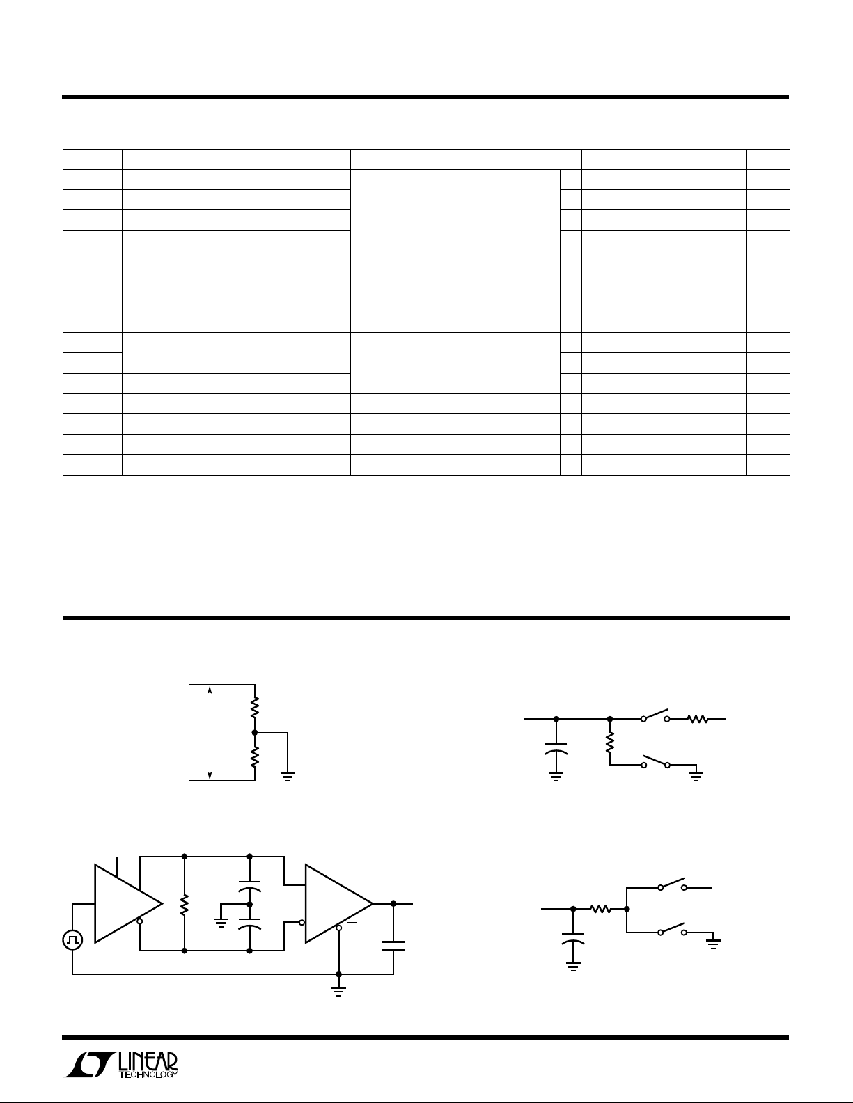
TEST CIRCUITS
A
R
V
OD
V
OC
R
B
Figure 1. Driver DC Test Load Figure 2. Receiver Timing Test Load
3V
DE
DI
A
B
LTC485 • F01
A
C
L1
R
DIFF
B
C
L2
RO
RE
15pF
LTC485 • F03
Note 3: All typicals are given for V
= 5V and TA = 25°C.
CC
Note 4: The LTC485 is guaranteed by design to be functional over a supply
voltage range of 5V ±10%. Data sheet parameters are guaranteed over the
tested supply voltage range of 5V ±5%.
RECEIVER
OUTPUT
OUTPUT
UNDER TEST
TEST POINT
C
RL
15pF
500Ω
C
L
S1
1k
V
CC
1k
S2
LTC485 • F02
S1
V
CC
S2
LTC485 • F02
Figure 3. Driver/Receiver Timing Test Circuit Figure 4. Driver Timing Test Load #2
3
LTC485
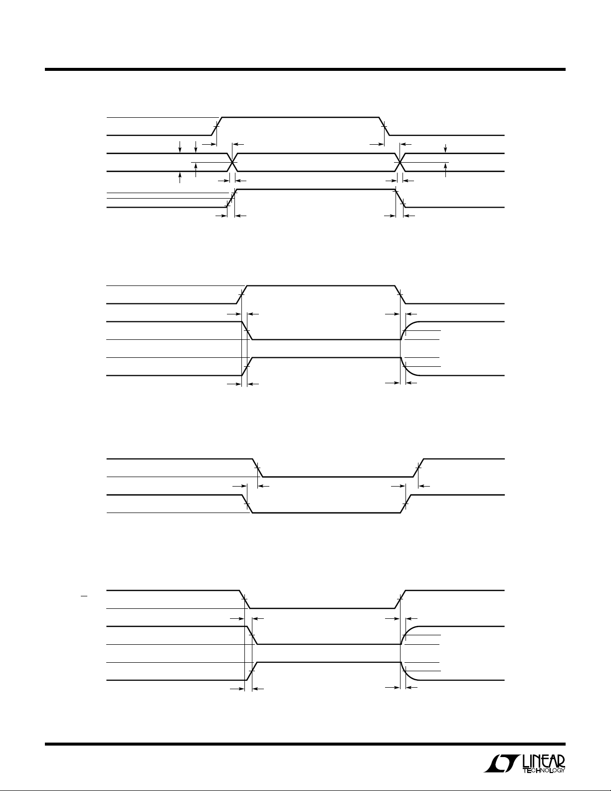
UW W
SWITCHI G TI E WAVEFOR S
DI
A, B
A, B
–V
3V
0V
B
A
V
O
0V
O
V
O
1/2 V
1.5V
O
10%
t
r
f = 1MHz, tr ≤ 10ns, tf ≤ 10ns
t
PLH
t
SKEW
80%
V
DIFF
= V(A) – V(B)
t
PLH
1.5V
1/2 V
O
t
SKEW
90%
20%
t
f
LTC485 • F05
Figure 5. Driver Propagation Delays
3V
DI
0V
5V
V
OL
V
OH
0V
t
1.5V
t
ZL
ZH
f = 1MHz, tr ≤ 10ns, tf ≤ 10ns
2.3V
2.3V
OUTPUT NORMALLY LOW
OUTPUT NORMALLY HIGH
t
t
1.5V
LZ
0.5V
0.5V
HZ
LTC485 • F06
A, B
Figure 6. Driver Enable and Disable Times
V
–V
OH
R
V
OL
V
OD2
OD2
t
PHL
1.5V
f = 1MHz, tr ≤ 10ns, tf ≤ 10ns
0V
OUTPUT
INPUT
1.5V
t
PLH
LTC485 • F07
Figure 7. Receiver Propagation Delays
3V
RE
0V
5V
R
R
0V
t
1.5V
f = 1MHz, tr ≤ 10ns, tf ≤ 10ns
t
ZL
1.5V
1.5V
ZH
OUTPUT NORMALLY LOW
OUTPUT NORMALLY HIGH
t
t
1.5V
LZ
0.5V
0.5V
HZ
LTC485 • F08
4
Figure 8. Receiver Enable and Disable Times
 Loading...