

Page 1

L DESIGN FEATURES
Ultralow Noise 15mm ×15mm × 2.8mm
µModule Step-Down Regulators Meet
the Class B of CISPR 22 and Yield
High Efficiency at up to 36V
by Judy Sun, Jian Yin, Sam Young and Henry Zhang
Introduction
Power supply designers face many
tradeoffs. Need high efficiency, large
conversion ratios, high power and
good thermal performance? Choose a
switching regulator. Need low noise?
Choose a linear regulator. Need it
all? Compromise. One compromise
is to follow a switcher with a linear
regulator (or regulators). Although this
cleans up the output noise relative to
a switcher-only solution, a good portion of the conducted and radiated
EMI remains—even if ferrite beads,
π filters, and LC filters are used. The
problem can always be traced back to
the switcher, where fast dI/dt transitions and high switching frequencies
Table 1. Feature comparison of ultralow noise µModule regulators
Feature LTM4606 LTM4612
These µModule step-down
regulators are designed
to achieve both high
power density and meet
EMC (electromagnetic
compatibility) standards.
The integrated ultralow
noise feature allows both
devices to pass the Class
B of CISPR 22 radiated
emission limit, thus
eliminating expensive EMI
design and lab testing.
lead to high frequency EMI, but
some applications, especially those
with large conversion ratios, require
a switcher.
Fortunately, the LTM4606 and
LTM4612 µModule regulators offer the
advantages of a switching regulator
while maintaining ultralow conducted
and radiated noise. These µModule
step-down regulators are designed to
achieve both high power density and
meet EMC (electromagnetic compatibility) standards. The integrated
ultralow noise feature allows both
devices to pass the Class B of CISPR
22 radiated emission limit, thus
eliminating expensive EMI design and
IN
V
IN
V
OUT
I
OUT
CISPR 22 Class B Compliant
Output Voltage Tracking and Margining
PLL Frequency Synchronization
±1.5% Total DC Error
Power Good Output
Current Foldback Protection
Parallel/Current Sharing
Low Input and Output Referred Noise
Ultrafast Transient Response
Current Mode Control
Programmable Soft-Start
Output Overvoltage Protection
Package 15mm × 15mm × 2.8mm 15mm × 15mm × 2.8mm
4.5V to 28V 5V to 36V
0.6V to 5V 3.3V to 15V
6A DC Typical, 8A Peak 5A DC Typical, 7A Peak
L L
L L
L L
L L
L L
L L
L L
L L
L L
L L
L L
L L
10
Linear Technology Magazine • January 2009
Page 2
DESIGN FEATURES L
+
INTERNAL
COMP
SGND
COMP
PGOOD
RUN
>1.9V = ON
<1V = OFF
MAX = 5V
MARG1
MARG0
MPGM
FCB
PLLIN
C
SS
INTV
CC
DRV
CC
TRACK/SS
V
FB
f
SET
50k
41.2k
R
FB
19.1k
50k
60.4k
V
OUT
5.1V
ZENER
POWER CONTROL
M1
V
IN
4.5V TO 28V
V
D
V
OUT
2.5V
AT 6A
M2
50k
22µF
1.5µF
C
IN
+
C
OUT
PGND
C
D
10k
4.7µF
INPUT
FILTER
NOISE
CANCEL-
LATION
LOAD CURRENT (A)
0
EFFICIENCY (%)
100
90
70
80
60
50
654321
1.2V
OUT
1.5V
OUT
2.5V
OUT
3.3V
OUT
5V
OUT
LOAD CURRENT (A)
0.0
EFFICIENCY (%)
75
0.5 1.0 1.5 2.0 2.5 3.0 3.5 4.0 4.5
65
90
70
95
60
55
85
80
24V
IN,
12V
OUT
DCM
CCM
P
GOOD
RUN
V
D
INTV
CC
DRV
CC
f
SET
TRACK/SS
COMP
FCB
MARG0
MARG1
MPGM
V
OUT
V
FB
V
IN
C4
0.01µF
C3
100pF
C
OUT1
22µF
25V
C
OUT2
180µF
16V
V
OUT
12V
4.5A
C1
10µF
50V
C
IN
10µF x 2
50V
V
IN
18V
TO 36V
PLLIN
CLOCK SYNC
ON/OFF
LTM4612
SGND PGND
MARGIN
CONTROL
R4
100k
R
SET
5.23k
R1
392k
5% MARGIN
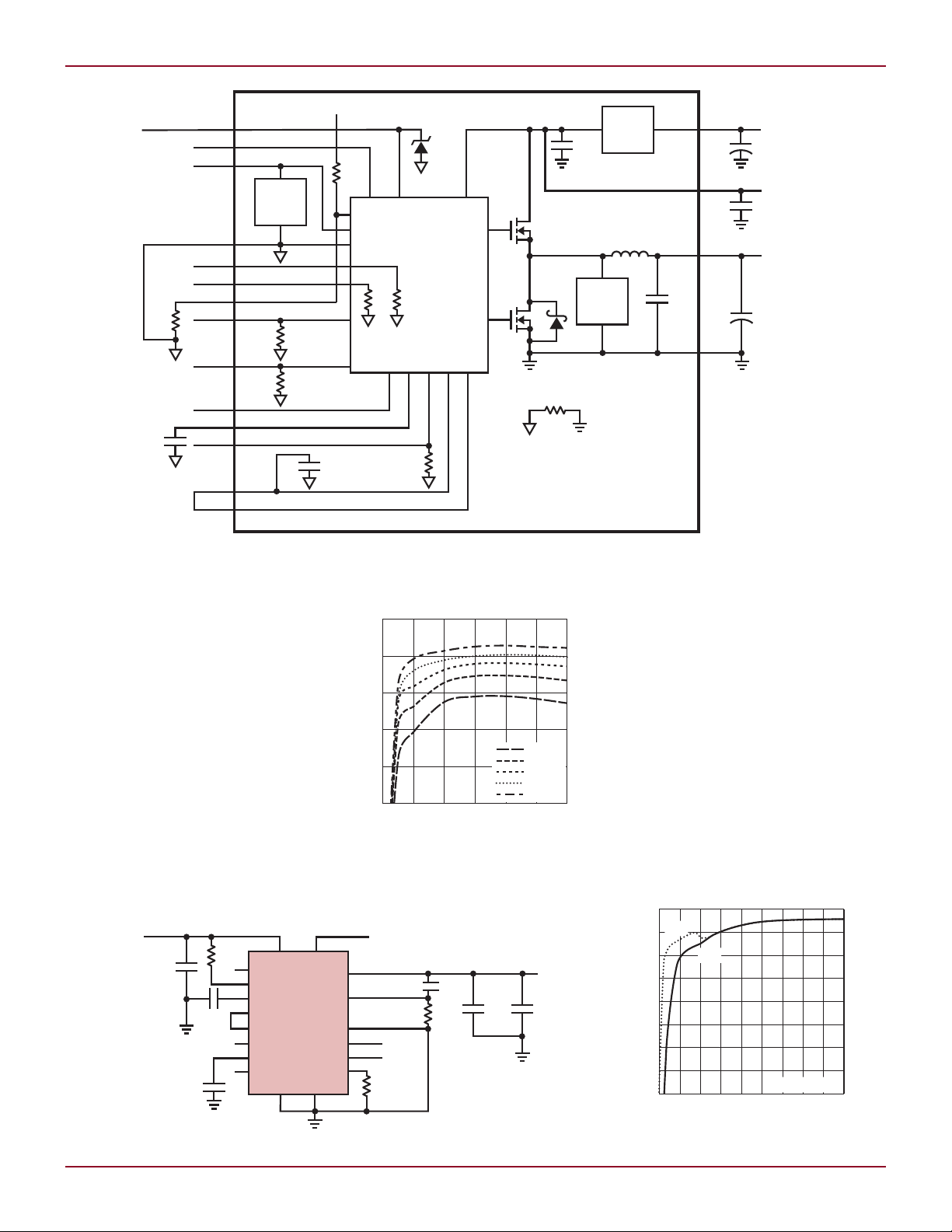
Figure 1. Simplified block diagram of the LTM4606 (LTM4612 is similar). Only a few
capacitors and resistors are required to build a complete wide-input-range regulator.
lab testing. See Table 1 for a feature
comparison of these two parts.
Both µModule regulators are offered in space saving, low profile and
thermally enhanced 15mm × 15mm ×
2.8mm LGA packages, so they can be
placed on the otherwise unused space
at the bottom of PC boards for highaccuracy point-of-load regulation. This
is not possible with linear regulators
Figure 2. Efficiency of the
LTM4606 with a 12V input.
that require a bulky cooling system.
Almost all support components are
integrated into the µModule package,
so layout design is relatively simple,
Figure 3. A few capacitors and resistors complete an 18V–36V input, 12V/4.5A output design.
Linear Technology Magazine • January 2009
requiring only a few input and output
capacitors.
For more output power, both parts
can be easily paralleled, where output
currents are automatically shared
due to the current mode control
structure.
Easy Power Supply Design
with Ultralow Noise
µModule Regulators
With a few external input and output capacitors, the LTM4612 can
deliver 4.5A of DC output current
Figure 4. Efficiency for the circuit in Figure 3.
11
Page 3

L DESIGN FEATURES
V
IN
50mV/DIV
97mV
P–P
13.8mV
P–P
V
OUT
5mV/DIV
2µs/DIVVIN = 5V
V
OUT
= 1.2V
I
LOAD
= 5A
CIN = 3×10µF/25V CERAMIC AND 1×150µF/25V ELECTROLITIC
C
OUT
= 1×100µF/25V AND 3×22µF/25V CERAMIC
SCOPE BW = 300MHz
V
IN
5mV/DIV
10.6mV
P–P
4.4mV
P–P
V
OUT
2mV/DIV
2µs/DIVVIN = 5V
V
OUT
= 1.2V
I
LOAD
= 5A
CIN = 3×10µF/25V CERAMIC AND 1×150µF/25V ELECTROLITIC
C
OUT
= 1×100µF/25V AND 3×22µF/25V CERAMIC
SCOPE BW = 300MHz
+
LT4606 OR LTC4612
V
D
V
IN
V
IN
L1
C3
10µF
C2
10µF
×3
C1
150µF
FREQUENCY (MHz)
0.15
0
SIGNAL AMPLITUDE (dBµV)
20
40
60
80
10
30
50
70
1 3010
CIS25QP
VIN = 24V
V
OUT
= 12V
Figure 5. Thermal image of an LTM4606
with 24V input and 3.3V output at 6A
Figure 6. Input π filter reduces
high frequency input noise.
Figure 3 shows a complete 18V–36V
VIN, 12V/4.5A V
LTM4612. Figure 4 shows the ef
design with the
OUT
-
ficiency.
Both parts offer good thermal performance with a large output load
current. Figure 5 shows the LTM4606
thermal image with 24V input and
3.3V output at 6A load current. The
maximum case temperature is only
73.5oC with the 20W output power.
Both include a number of built-in
features, such as controllable softstart, RUN pin control, output voltage
tracking and margining, PGOOD
indicator, frequency adjustment and
external clock synchronization. Efficiency can be further improved by
applying an external gate driver voltage
to the DRVCC pin, especially in high
VIN applications. Discontinuous mode
operation can be enabled to increase
the light load efficiency.
Figure 7. Input and output noise of comparable
µModule regulator without low noise feature
Figure 9. The conducted EMI test of the LTM4612 passes EMI standard CISPR 25 level 5.
and the LTM4606 can deliver 6A. The
LTM4612’s programmable output can
be precisely regulated in a 3.3V-to-15V
range from a 4.5V-to-36V input; the
LTM4606 can produce 0.6V to 5V from
a 4.5V-to-28V range. With current
mode control and optimized internal
compensations, both offer stable
output even in the face of significant
load transients.
12
Figure 8. Input and output noise of LTM4606
µModule regulator is significantly lower than
the regulator in Figure 7.
Figure 1 shows the simplified block
diagram of the LTM4606 with an input
from 4.5V to 28V and 2.5V/6A output.
Figure 2 shows the efficiency test
curves with 12V input voltage under
CCM mode. About 92% efficiency is
achieved at full load with LTM4606,
running at 900kHz switching frequency.
Reduce Conducted EMI
Conducted input and output noise of
switching regulators (aka ripple) is
usually a problem when the regulator
operates at high frequency, which is
common in space-constrained applications. The LTM4606 and LTM4612
reduce peak-to-peak ripple at the
input by integrating a high frequency
inductor as shown in Figure 6. The
external input capacitors at the VD
and VIN pins form a high frequency
input π filter. This effectively reduces
conductive EMI coupling between the
module and the main input bus.
Since most input RMS current flows
into capacitor C3 at the VD pin, C3
should have enough capacity to handle
the RMS current. A 10µF ceramic capacitor is recommended. To effectively
attenuate EMI, place C3 as close as
possible to the VD pin. The ceramic
capacitors C2 mainly determine the
ripple noise attenuation, so the capacitor value can be varied to meet the
different input ripple requirements.
C1 is only needed if the input source
impedance is compromised by long
inductive leads or traces.
Since these µModule regulators
are used in a buck circuit topology,
the lowpass filter formed by the output inductor L and capacitor C
Linear Technology Magazine • January 2009
OUT
Page 4

FREQUENCY (MHz)
0
EMISSIONS LEVEL (dBµV/m)
10
30
50
90
70
10009008007006005004003002001000
CISPR22, CLASS B
FREQUENCY (MHz)
0
EMISSIONS LEVEL (dBµV/m)
10
30
50
90
70
10009008007006005004003002001000
CISPR22, CLASS B
VIN = 12V
V
OUT
= 2.5V
I
LOAD
= 6A
FREQUENCY (MHz)
0
EMISSIONS LEVEL (dBµV/m)
10
30
50
90
70
10009008007006005004003002001000
CISPR22, CLASS B
VIN = 12V
V
OUT
= 2.5V
I
LOAD
= 6A
FREQUENCY (MHz)
0
EMISSIONS LEVEL (dBµV/m)
10
30
50
90
70
10009008007006005004003002001000
CISPR22, CLASS B
VIN = 24V
V
OUT
= 12V
I
LOAD
= ??A
RESISTIVE LOAD
LTM4606 µMODULE
REGULATOR
DC POWER SUPPLY
DESIGN FEATURES L
Figure 10. Setup of the radiated emission scan
can similarly reduce the conducted
output EMI.
To show the relative noise attenuation of these µModule regulators, a
similar module without the low noise
feature is compared to the LTM4606
for input and output noise, as shown in
Figure 7 and Figure 8. Both modules
are tested from 5V input to 1.2V output
at 5A with resistive loads. The same
board layout and I/O capacitors are
used in the comparison. The results
show that the LTM4606 produces
much lower input and output noise,
with a nearly 10× reduction of the
peak-to-peak input noise and better
than 3× reduction of the output noise
compared to the similar module in
Figure 7.
Figure 9 shows the conducted EMI
testing results for the LTM4612 with
a 24V VIN, 12V/5A V
, which ac-
OUT
commodates the EMI standard CISPR
25 level 5. The input capacitance for
this test comes from 4 × 10µF/50V
ceramics plus a single 150µF/50V
electrolytic.
Reduce Radiated EMI
Switching regulators also produce
radiated EMI, caused by the high dI/
dt signals inherent in high efficiency
regulators. The input π filter helps to
limit radiated EMI caused by high dI/dt
loops in the immediate module area,
but to further attenuate radiated EMI,
the LTM4606 and LTM4612 include an
optimized gate driver for the MOSFET
and a noise cancellation network.
To test radiated EMI, several setups are tested in a 10-meter shielded
chamber as shown in Figure 10. To
ensure a low baseline radiated noise,
Linear Technology Magazine • January 2009
Figure 11. Radiated emission scan of baseline noise (no switching regulator module)
Figure 12. Radiated emission peak scan of a typical module without the low noise features.
Figure 13. The radiated EMI test of the LTM4606 passes EMI standard CISPR 22 Class B.
Figure 14. The radiated EMI test of the LTM4612 passes EMI standard CISPR 22 Class B.
13
Page 5

L DESIGN FEATURES
Table 2. Noise margins are good for radiated emission results shown in Figure 13
EUT
Frequency
(MHz)
134.31 H 354 364 1.3 11.428 0 1.532 0 14.26 30 15.74
119.96 V 184 110 3.5 12.694 0 1.456 0 17.65 30 12.35
160.02 H 0 354 0.5 10.499 0 1.793 0 12.792 30 17.208
174.37 H 0 100 1.2 9.638 0 1.944 0 12.782 30 17.218
224.28 V 0 100 –1.87 10.586 0 2.044 0 10.76 30 19.24
263.63 H 0 371 –4.72 12.6 0 2.385 0 10.265 37 26.735
Antenna
Polarization
Azimuth
(Degrees)
a linear DC power supply is used
for the input, and a resistive load is
employed on the output. The baseline
noise is checked with the power supply
providing a DC current directly to the
resistive load. The baseline emission
scan results are shown in Figure 11.
There are two traces in the plot, one
for the vertical and horizontal orientations of the receiver antenna.
Figure 12 shows the peak scan re
sults of a µModule buck regulator—not
the LTM4606 or LTM4612—without
the integrated low noise feature. The
scan results show that the noise below
350MHz is produced by the µModule
switching regulator, when compared
to the baseline noise level. Radiated
EMI here does not meet the Class B
of CISPR 22 (quasi-peak) radiated
emission limit.
Antenna
Height
(cm)
Uncorrected
Amplitude
(dBµV)
Pre-Amp
ACF
(dB/m)
In contrast, Figure 13 shows the
peak scan results of the low noise
LTM4606 module. To ensure enough
margin to the quasi-peak limit for
different operation conditions, the
six highest noise points are checked
as shown in the table of Figure 13
using the quasi-peak measurement.
The results show that it has more
than 12dBµV margin below the Class
-
B of CISPR 22(quasi-peak) radiated
emission limit.
Figure 14 shows the results for the
LTM4612 meeting the Class B of CISPR
22 radiated emission limit at 24V VIN,
12V/5A V
OUT
.
Conclusion
The LTM4606 and LTM4612 µModule
regulators offer all of the high performance benefits of switching regulators
minus the noise issues. The ultralow
Gain
(dB)
Corrected
CBL
DCF
(dB)
(dB)
Amplitude
(dBµV)
Limit
(dBµV)
Margin
noise optimized design produces radiated EMI performance with enough
margin below the Class B of CISPR 22
limit to simplify application in noisesensitive environments.
Design is further simplified by
exceptional thermal performance,
which allows them to achieve high
efficiency and a compact form factor. A low profile 15mm × 15mm ×
2.8mm package contains almost all
of the support components—only a
few input and output capacitors are
required to complete a design. Several
µModule regulators can be easily run
in parallel for more output power. The
versatility of these parts is rounded out
by optional features such as soft-start,
RUN pin control, output voltage tracking and margining, PGOOD indicator,
frequency adjustment and external
clock synchronization.
L
(dB)
LTC6652, continued from page 9
output headroom while fully loaded,
and they require less headroom with a
reduced load or while sinking current.
Popular application requirements,
such as a 2.5V reference operating
on a 3V supply, or a 4.096V reference
operating on a 5V supply, are easily
accommodated. For high input voltage requirements, all voltage options
work up to 13.2V. Regardless of input
voltage the LTC6652 maintains its
excellent accuracy as shown in the
line regulation plot in Figure 6. A plot
of the dropout voltage for both sourcing and sinking current is shown in
Figures 7a and 7b, respectively.
14
Superior Performance
While many references share some
features of the LTC6652, it’s difficult
to find any that include all the features
at the same level of performance and
reliability. Additional features include
low noise, good AC PSRR, and excellent load regulation (both sourcing and
sinking current). Low power consumption and a shutdown mode round out
the feature list.
Conclusion
The LTC6652 reference family is
designed and factory trimmed to
yield exceptional drift and accuracy
performance. The entire family is
guaranteed and production tested at
–40°C, 25°C and 125°C to ensure dependable performance in demanding
applications. Low thermal hysteresis
and low long-term drift reduce or
eliminate the need for field calibration. The small 8-lead MSOP package
and sparse capacitor requirements
minimize required board space. The
wide input range from 2.7V to 13.2V
and seven output voltage options will
tackle the needs of most precision
reference users.
Linear Technology Magazine • January 2009
L
 Loading...