

FEATURES
LTC4556
Smart Card Interface
with Serial Control
U
DESCRIPTIO
■
Electrical Specifications Are ISO7816-3 and EMV
Compatible
■
Control/Status Serial Port May be Daisy-Chained
for Multicard Applications
■
Automatic Shutdown on Electrical Faults
■
Buck Boost Charge Pump Generates 5V, 3V or 1.8V
Outputs (Smart Card Classes A, B and C)
■
Automatic Level Translation
■
Dynamic Pull-Ups Deliver Fast Signal Rise Times*
■
Supervisory Functions Prevent Smart Card Faults
■
Low Operating Current: 250µA Typical
■
VIN: 2.7V to 5.5V
■
Ultralow Shutdown Current
■
>10kV ESD on Smart Card Pins
■
Small 24-Pin 4mm × 4mm QFN Package
U
APPLICATIO S
■
Handheld Payment Terminals
■
Pay Telephones
■
ATM Machines
■
POS Terminals
■
Computer Keyboards
■
Multiple S.A.M. Sockets
The LTC®4556 provides all necessary power control, level
translation and supervisory functions for a smart card or
S.A.M. card interface. The part contains a low noise charge
pump** plus LDO for generating VCC power, as well as all
necessary level shifting circuitry.
The card voltage can be set to either 1.8V, 3V or 5V. The
LTC4556 includes a card detection channel with automatic
debounce circuitry. To reduce wiring costs, the LTC4556
interfaces to a microcontroller via a simple 4-wire serial
interface. Multiple devices may be connected in daisychain fashion so that the number of wires to the card
socket board is independent of the number of sockets.
Status data is returned over the same interface.
Extensive security features ensure proper deactivation
sequencing in the event of a supply fault or a smart card
electrical fault. The smart card pins can withstand greater
than 10kV ESD in-situ with no additional components.
The LTC4556 is available in a small, low profile (0.75mm),
4mm × 4mm QFN package.
, LTC and LT are registered trademarks of Linear Technology Corporation.
*U.S. Patent No. 6,356,140
**U.S. Patent No. 6,411,531
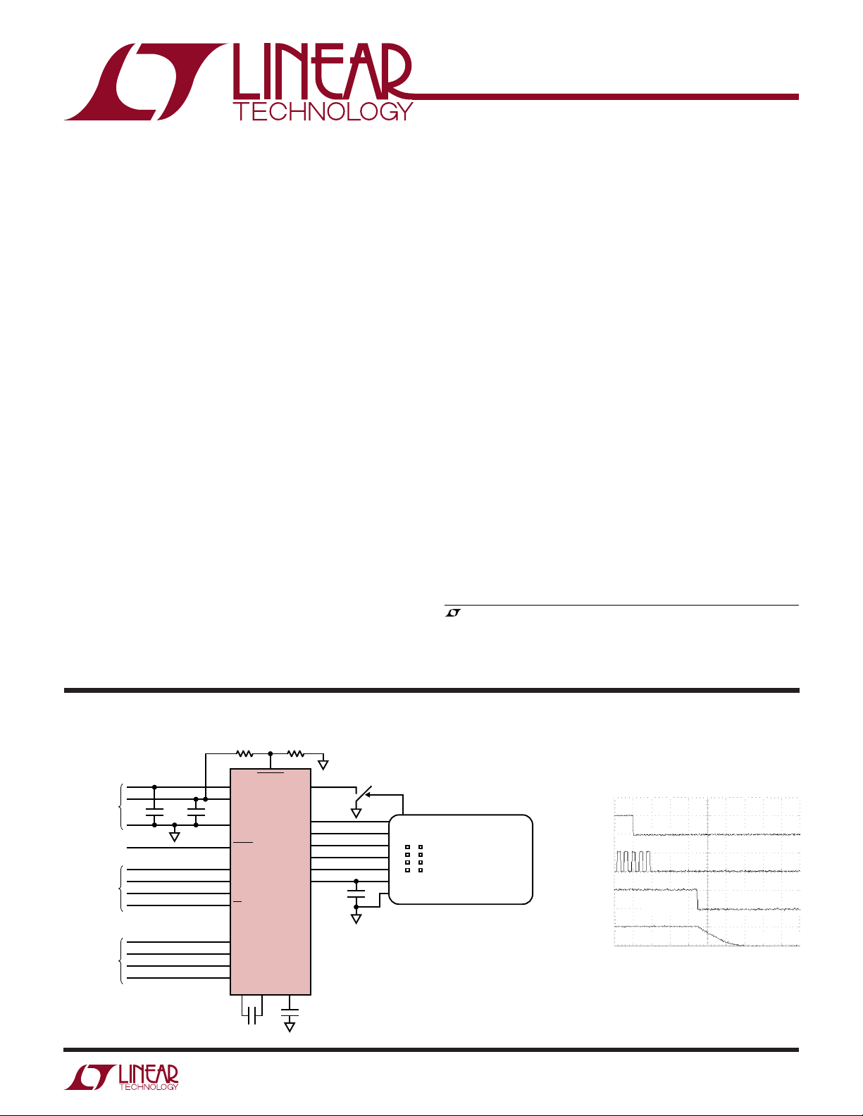
TYPICAL APPLICATIO
240k
UNDERV
1
DV
CC
10
V
INPUT
POWER
4-WIRE
COMMAND
INTERFACE
4-WIRE
CARD
INTERFACE
1µF0.1µF
BATT
8
GND
6
FAULT
21
D
IN
22
D
OUT
23
SCLK
24
LD
2
DATA
3
R
IN
4
SYNC
5
ASYNC
C+C–CPO
LTC4556
1µF
U
180k
20
PRES
RST
CLK
V
12911
19
18
C8
17
C4
16
I/O
15
14
13
CC
1µF
1µF
SMART CARD
4556 TA01
RST
5V/DIV
CLK
5V/DIV
5V/DIV
V
5V/DIV
I/O
CC
Deactivation Sequence
10µs/DIV
4556 G11.eps
4556f
1
LTC4556
WW
W
ABSOLUTE AXI U RATI GS
V
, DVCC, CPO, FAULT,
BATT
U
(Note 1)
UNDERV to GND....................................... –0.3V to 6.0V
PRES, DATA, RIN, SYNC, ASYNC,
LD, DIN, SCLK to GND ............... –0.3V to (DVCC + 0.3V)
I/O, CLK ....................................... –0.3V to (VCC + 0.3V)
UUW
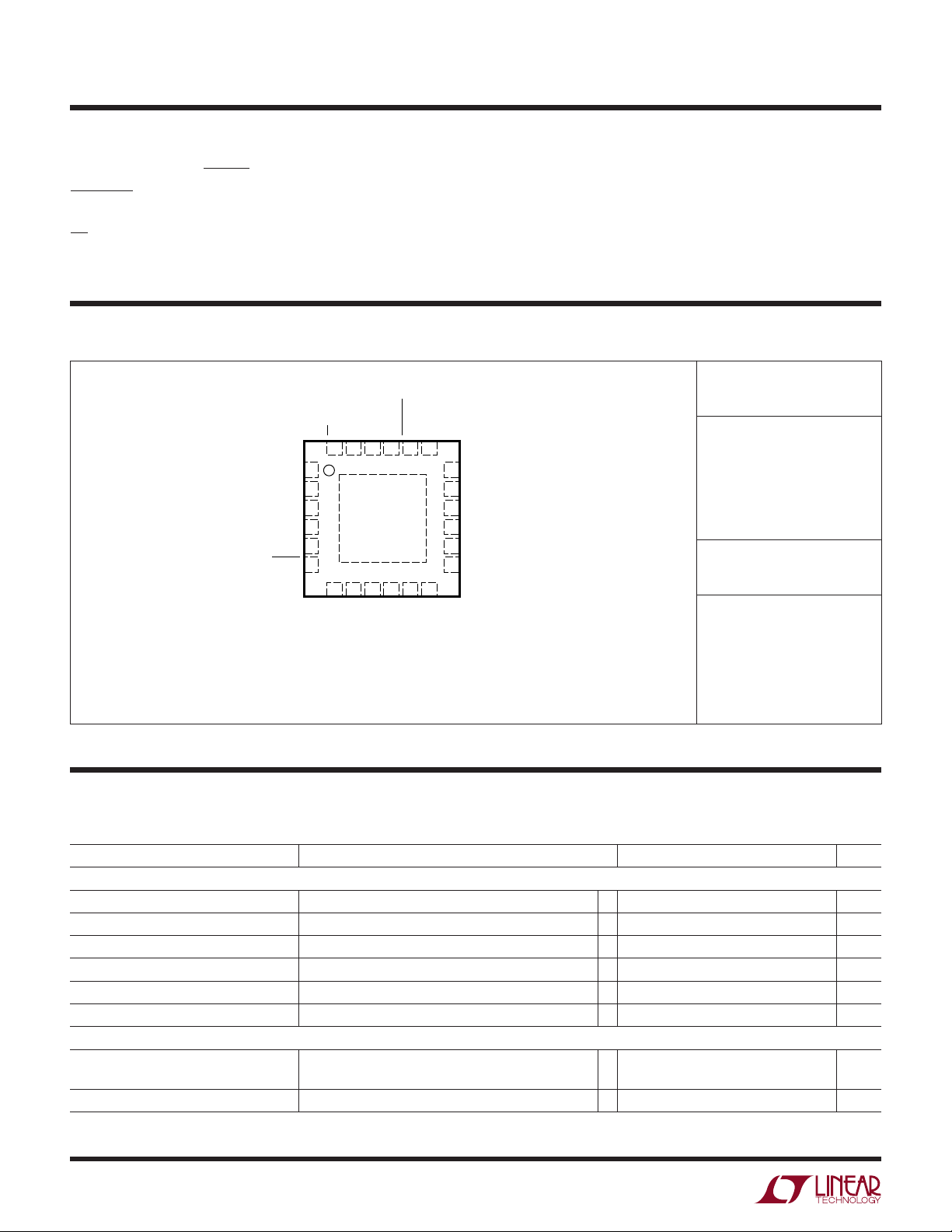
PACKAGE/ORDER I FOR ATIO
TOP VIEW
OUTDIN
LD
SCLK
D
UNDERV
PRES
24 23 22 21 20 19
DV
1
CC
DATA
2
R
3
IN
SYNC
4
ASYNC
5
FAULT
6
24-LEAD (4mm × 4mm) PLASTIC QFN
T
JMAX
EXPOSED PAD (PIN 25) IS SGND.
MUST BE SOLDERED TO PCB
25
7 8 9 10 11 12
–
C
NC
GND
UF PACKAGE
= 125°C, θJA = 37°C/W
BATT
V
18
17
16
15
14
13
+
C
CPO
ICC (Note 5) .......................................................... 65mA
VCC Short-Circuit Duration............................... Indefinite
Operating Temperature Range (Note 4) .. – 40°C to 85°C
Storage Temperature Range ................. –65°C to 125°C
ORDER PART
NUMBER
LTC4556EUF
C8
C4
I/O
RST
CLK
V
CC
UF PART
MARKING
4556
Consult LTC Marketing for parts specified with wider operating temperature ranges.
ELECTRICAL CHARACTERISTICS
temperature range, otherwise specifications are at TA = 25°C. V
PARAMETER CONDITIONS MIN TYP MAX UNITS
Input Power Supply
V
Operating Voltage ● 2.7 5.5 V
BATT
I
Operating Current VCC = 5V, ICC = 0µA ● 250 400 µA
VBATT
I
Shutdown Current No Card Present, V
VBATT
DVCC Operating Voltage ● 1.7 5.5 V
I
Operating Current ● 525µA
DVCC
I
Shutdown Current ● 0.2 1.5 µA
DVCC
Charge Pump
R
5V Mode Open-Loop V
OLCP
Output Resistance
CPO Turn On Time ICC = 0mA, 10% to 90% ● 0.6 1.5 ms
= 3.075V, I
BATT
The ● denotes the specifications which apply over the full operating
= 3.3V, DVCC = 3.3V unless otherwise noted.
BATT
= 0V ● 0.5 1.75 µA
CPO
= ICC = 60mA, (Note 3) ● 8.2 17 Ω
CPO
4556f
2
LTC4556
ELECTRICAL CHARACTERISTICS
temperature range, otherwise specifications are at TA = 25°C. V
The ● denotes the specifications which apply over the full operating
= 3.3V, DVCC = 3.3V unless otherwise noted.
BATT
SYMBOL CONDITIONS MIN TYP MAX UNITS
Smart Card Supply
VCC Output Voltage 5V Mode, 0 < ICC < 60mA ● 4.65 5.0 5.35 V
3V Mode, 0 < I
1.8V Mode, 0 < I
< 50mA ● 2.75 3.0 3.25 V
CC
< 30mA ● 1.65 1.8 1.95 V
CC
VCC Turn On-Time ICC = 0mA, 10% to 90% ● 0.8 1.5 ms
Undervoltage Detection Relative to Nominal Output ● –9 –5 –2.5 %
Overcurrent Detection ● 60 110 150 mA
Smart Card Detection
Debounce Time ( PRES to D7) ● 15 32 60 ms
PRES Pull-Up Current V
Deactivation Time ( RST to VCC = 0.4V) ICC = 0mA, C
= 0 ● 1 2.5 µA
PRES
= 1µF ● 100 250 µs
VCC
CLK (Non-Bidirectional Modes)
Low Level Output Voltage (VOL), (Note 2) Sink Current = –200µA ● 0.2 V
High Level Output Voltage (VOH), (Note 2) Source Current = 200µA ● VCC – 0.2 V
Rise/Fall Time, (Note 2) Loaded with 50pF, 10% to 90% ● 16 ns
CLK Frequency, (Note 2) ● 10 MHz
RST, C4, C8
Low Level Output Voltage (VOL), (Note 2) Sink Current = –200µA ● 0.2 V
High Level Output Voltage (VOH), (Note 2) Source Current = 200µA ● VCC – 0.2 V
Rise/Fall Time, (Note 2) Loaded with 50pF, 10% to 90% ● 100 ns
I/O, CLK (CLK Specifications in Bidirectional Mode Only)
Low Level Output Voltage (VOL), (Note 2) Sink Current = –1mA (V
High Level Output Voltage (VOH), (Note 2) Source Current = 20µA (V
= V
V
SYNC
DVCC
)
DATA
DATA
= 0V or V
= V
DVCC
= 0V) ● 0.3 V
SYNC
or ● 0.85 • V
CC
Rise/Fall Time, (Note 2) Loaded with 50pF, 10% to 90% ● 500 ns
Short Circuit Current, (Note 2) V
DATA
= 0V or V
= 0V ● 510mA
SYNC
DATA, SYNC (SYNC Specifications in Bidirectional Mode Only)
Low Level Output Voltage (VOL) Sink Current = –500µA (V
High Level Output Voltage (VOH) Source Current = 20µA (V
= 0V or V
I/O
= VCC or V
I/O
= 0V) ● 0.3 V
CLK
= VCC) ● 0.8 • DV
CLK
CC
Rise/Fall Time Loaded with 50pF ● 500 ns
RIN, DIN, SCLK, LD, SYNC, ASYNC (SYNC Specifications for Non-Bidirectional Mode)
Low Input Threshold (VIL) ● 0.15 • DV
High Input Threshold (VIH) ● 0.85 • DV
CC
CC
Input Current (IIH/IIL) ● –1 1 µA
D
OUT
Low Level Output Voltage (VOL) Sink Current = –200µA ● 0.3 V
High Level Output Voltage (VOH) Source Current = 200µA ● DVCC – 0.3 V
UNDERV
Threshold ● 1.17 1.23 1.29 V
Leakage Current V
= 3.3V ● 50 nA
UNDERV
V
V
V
V
4556f
3
LTC4556
ELECTRICAL CHARACTERISTICS
temperature range, otherwise specifications are at TA = 25°C. V
The ● denotes the specifications which apply over the full operating
= 3.3V, DVCC = 3.3V unless otherwise noted.
BATT
PARAMETER CONDITIONS MIN TYP MAX UNITS
FAULT
Low Level Output Voltage (VOL) Sink Current = –200µA ● 0.005 0.3 V
Leakage Current V
= 5.5V ● 1 µA
FAULT
Serial Port Timing
t
DS
t
DH
t
DD
t
L
t
H
t
LW
t
CL
t
LC
Note 1: Absolute Maximum Ratings are those values beyond which the life
of a device may be impaired.
Note 2: This specification applies to all three smart card voltage classes:
1.8V, 3V and 5V.
Note 3: R
(I
CC
DIN Valid to SCLK Setup 8 ns
DIN Valid to SCLK Hold 8 ns
D
Output Delay C
OUT
= 15pF 15 60 ns
LOAD
SCLK Low Time 50 ns
SCLK High Time 50 ns
LD Pulse Width 50 ns
SCLK to LD 50 ns
LD to SCLK 0ns
Note 4: The LTC4556E is guaranteed to meet performance specifications
from 0°C to 70°C. Specifications over the –40°C to 85°C operating
temperature range are assured by design, characterization and correlation
with statistical process controls.
OLCP
≡ (2V
BATT
– V
CPO
)/I
CPO
) and minimum supply voltage V
; V
will depend upon total load
CPO
. See Figure 6.
BATT
Note 5: Based on long term current density limitation.
UW
TYPICAL PERFOR A CE CHARACTERISTICS
I/O and CLK Short-Circuit Current
vs Temperature
No Load Supply Current vs V
500
TA = 25°C
= 0µA
I
CC
400
300
200
SUPPLY CURRENT (µA)
100
0
2.7 3.1 3.5 3.9 4.3 4.7 5.1 5.5
VCC = 5V
VCC = 3V
VCC = 1.8V
V
SUPPLY VOLTAGE (V)
BATT
BATT
4556 G01
(CLK in Bidirectional Mode)
6.0
DVCC = V
V
CC
5.5
5.0
4.5
4.0
SHORT-CIRCUIT CURRENT (mA)
3.5
–40
= 3.3V
BATT
= 5V
CLK
I/O
–15 10 35 60 85
TEMPERATURE (°C)
4556 G02
Charge Pump Open-Loop Output
Resistance vs Temperature
(2V
– V
BATT
10
V
= 2.7V
BATT
= 4.9V
V
CPO
9
8
7
OUTPUT RESISTANCE (Ω)
6
–15 10 35 60 85
–40
) / I
CPO
CPO
TEMPERATURE (°C)
4556 G03
4
4556f
UW
TEMPERATURE (°C)
–40
–15 10 35 60 85
I/O LOW OUTPUT VOLTAGE (mV)
4556 G06
200
175
150
125
100
V
DATA
= V
SYNC
= 0V
I
OL
= –1mA
V
BATT
= 3V
VCC = 1.8V
VCC = 3V, 5V
V
DVCC
SUPPLY VOLTAGE (V)
2.7 3.1 3.5 3.9 4.3 4.7 5.1 5.5
SUPPLY CURRENT (µA)
4556 G09
1.0
0.8
0.6
0.4
0.2
0
TA = 25°C
TA = 85°C
TA = –40°C
V
BATT
= V
DVCC
TYPICAL PERFOR A CE CHARACTERISTICS
LTC4556
VCC Overcurrent Shutdown
Threshold vs Temperature
140
V
= 3.3V
BATT
130
120
VCC = 5V, CPO = 5.5V
110
100
LOAD CURRENT (mA)
90
80
–15 10 35 60 85
–40
VCC = 1.8V, CPO = 4V
TEMPERATURE (°C)
Extra Input Current vs
Load Current (I
6
V
= 3.3V
BATT
T
= 25°C
A
5
4
3
BATT
VCC = 3V, CPO = 5.5V
4556 G04
– 2ICC)
Card Detection Debounce Time vs
V
Supply Voltage
BATT
50
45
40
35
DEBOUNCE TIME (ms)
30
25
2.7 3.1 3.5 3.9 4.3 4.7 5.1 5.5
V
SUPPLY VOLTAGE (V)
BATT
V
Shutdown Current vs
BATT
TA = 85°C
TA = 25°C
TA = –40°C
Supply Voltage
3.0
V
= V
BATT
DVCC
2.5
2.0
1.5
TA = –40°C
TA = 25°C
Bidirectional Channel (I/O) Low
Output Level vs Temperature
4556 G05
DVCC Shutdown Current vs Supply
Voltage
2
EXTRA INPUT CURRENT (mA)
1
0
0.01 1 10
Charge Pump and LDO Activation Deactivation Sequence Data – I/O Channel
V
CPO
5V/DIV
5V/DIV
5V/DIV
V
CC
I/O
0.1 100
LOAD CURRENT (mA)
1ms/DIV 4556 G10 10µs/DIV 4556 G11.eps
4556 G07
1.0
SUPPLY CURRENT (µA)
0.5
0
2.7 3.1 3.5 3.9 4.3 4.7 5.1 5.5
RST
5V/DIV
CLK
5V/DIV
I/O
5V/DIV
V
5V/DIV
V
SUPPLY VOLTAGE (V)
BATT
CC
TA = 85°C
4556 G08
I/O
2V/DIV
DATA
2V/DIV
100ns/DIV
4556 G12
4556f
5

LTC4556
UUU
PI FU CTIO S
DVCC (Pin 1): Power. Reference voltage for the control
logic.
DATA (Pin 2): Input/Output. Microcontroller side data I/O
pin. The DATA pin provides the bidirectional communication path to the smart card. The card may be selected to
communicate via the DATA pin. If several LTC4556s are
connected in parallel, the DATA pin can be made high
impedance by selecting neither card socket. The C4 and C8
synchronous card pins can be selected to connect to the
DATA pin via the serial port (see Table 4).
RIN (Pin 3): Input. The RIN pin supplies the RST signal to
the smart card. It is level shifted and transmitted directly
to the RST pin of a selected card. When the card is
deselected, the RST pin is latched at its current state.
SYNC (Pin 4): Input-Input/Output. The SYNC pin provides
the clock input for synchronous smart cards. When a
synchronous card is selected, its CLK pin follows SYNC
directly. When a synchronous card is deselected, the CLK
pin is latched at its current state. In bidirectional mode, the
SYNC pin becomes an input/output with the smart card
CLK pin.
ASYNC (Pin 5): Input. The ASYNC pin provides the clock
input for asynchronous cards and should be connected to
a free running clock. The clock signal to the smart card can
be a ÷1, ÷2, ÷4 or ÷8 version of the signal on ASYNC.
Asynchronous cards can also be placed in clock stop
mode with the clock stopped either high or low.
FAULT (Pin 6): Output. The FAULT pin can be used as an
interrupt to a microcontroller to indicate when a fault has
occurred. It is an open drain output, which is logically
equivalent to D4 . (See Table 1)
NC (Pin 7): No Connection to chip. May be grounded.
GND (Pin 8): Ground. Power ground for the chip. This pin
should be connected directly to a low impedance ground
plane.
CPO (Pin 12): Charge Pump. CPO is the output of the
charge pump. When the smart card requires power, the
charge pump will charge CPO to either 3.7V or 5.35V
depending on what smart card voltage is required. A low
impedance 1µF X5R or X7R ceramic capacitor is required
on CPO.
VCC (Pin 13): Card Socket. The V
nected to the VCC pin of the smart card socket. The
activation of the VCC pin is controlled by the serial port (see
Tables 1 and 2) and can be set to 0V, 1.8V, 3V or 5V.
CLK (Pin 14): Card Socket. The CLK pin should be connected to the CLK pin of the smart card socket. The CLK
signal can be derived from either the SYNC input or the
ASYNC input depending on which type of card is being
accessed. The card type is selected via the serial port (see
Tables 1 and␣ 3). In bidirectional mode, the CLK pin becomes an input/output with the microcontroller side
SYNC pin.
RST (Pin 15): Card Socket. This pin should be connected
to the RST pin of the smart card socket. The RST signal is
derived from the RIN pin. When the card is selected, its
RST pin follows RIN. When the card is deselected, the RST
pin holds the current value on RIN.
I/O (Pin 16): Card Socket. The I/O pin connects to the I/O
pin of the smart card socket. When the smart card is
selected, its I/O pin connects to the DATA pin. When the
smart card is deselected, its I/O pin returns to the idle
state (H).
C4, C8 (Pins 17, 18): Card Socket. These pins connect to
the C4 and C8 pins of synchronous memory cards on the
smart card socket. The signal for these pins is unidirectional and can only be sent to the card. Data for C4 and C8
is transmitted via the DATA pin and may be selected in
place of I/O via the serial port (see Table 4). When either
C4 or C8 is selected, it will follow the DATA pin. When it is
deselected, it will remain latched at its current state.
pin should be con-
CC
C–, C+ (Pins 9, 11): Charge Pump. Charge pump flying
capacitor pins. A 1µF X5R or X7R ceramic capacitor
should be connected from C+ to C–.
V
(Pin 10): Power. Supply voltage for analog and
BATT
power sections of the LTC4556.
6
PRES (Pin 19): Card Socket. The PRES pin is used to
detect the presence of a smart card. It should be connected
to a normally open detection switch on the smart card
acceptor’s socket. This pin has a pull-up current source
on-chip so no external components are required.
4556f

UUU
PI FU CTIO S
LTC4556
UNDERV (Pin 20): Input. The UNDERV pin provides
security by supplying a precision undervoltage threshold
for external supply monitoring. An external resistive voltage divider programs the desired undervoltage threshold.
Once UNDERV falls below 1.23V, the LTC4556 automatically begins the deactivation sequence.
If external supply monitoring is not required, the UNDERV
pin should be connected to either V
BATT
or DVCC.
DIN (Pin 21): Input. Input for the serial port. Command
data is shifted into DIN synchronously with SCLK. DIN can
be connected directly to a microcontroller or the D
OUT
pin
of another LTC4556 or LTC1955 for daisy chained
operation.
D
(Pin 22): Output. Output for the serial port. Smart
OUT
card status data is shifted out of D
synchronously with
OUT
W
BLOCK DIAGRA
CHARGE PUMP
–
C+C
11 9
CHARGE
PUMP
SCLK. D
can be connected directly to a microcontroller
OUT
or the DIN pin of another LTC4556 or LTC1955 for daisy
chained operation.
SCLK (Pin 23): Input. The SCLK pin clocks the serial port.
Each new data bit is received on the rising edge of SCLK.
SCLK should be left high during idle times and should not
be clocked when LD is low.
LD (Pin 24): Input. The falling edge of this pin loads the
current state of the shift register into the command register. Command changes to the smart card will be updated
on the falling edge of LD. The rising edge of LD latches
status information into the shift register for the next read/
write cycle.
SGND (Pin 25): Exposed Pad. Must be soldered to PCB
Ground.
V
GND
8
BATT
10 12
CPO
SMART
CARD
COMMUNICATIONS
SERIAL PORT
COMMAND/STATUS
DATA
DATA
ASYNC
SYNC
D
SCLK
R
D
OUT
1.23V
13
V
CC
16
I/O
17
C4
SMART
6
1
4556 BD
C8
CLK
RST
PRES
FAULT
DV
CC
UNDERV
CARD
SOCKET
DIGITAL
SUPPLY
4556f
18
14
15
19
20
+
–
LDO
2
5
4
3
IN
21
IN
22
23
24
LD
CLOCK
CONTROL
LOGIC
RESET
CONTROL
LOGIC
STATUS DATA
SHIFT REGISTER
COMMAND LATCH
τ
–
+
7

LTC4556
OPERATIO
U
Serial Port
The microcontroller compatible serial port provides all of
the command and control inputs for the LTC4556 as well
as the status of the smart card. Data on the DIN input is
loaded on the rising edge of SCLK. D7 is loaded first and
D0 last. At the same time the command bits are being
shifted into the DIN input, the status bits are being shifted
out of the D
D
on the rising edge of SCLK. Once all bits have been
OUT
output. The status bits are presented to
OUT
clocked into the shift register, the command data is loaded
into the command latch by bringing LD low. At this time
the command latch is updated and the LTC4556 will begin
to act on the new command set. When LD is low, the shift
register is transparent to the status data of the smart card
channel. The status data is latched into the shift register on
the rising edge of LD. SCLK should be held in the high state
when idle and should only be clocked when LD is high.
Likewise LD should only be brought high when SCLK is
high. Figure 2 shows the operation of the serial port.
Multiple LTC4556s may be daisy chained together by
connecting the D
pin of one LTC4556 to the DIN pin of
OUT
another. Figure 7 shows an example of an LTC4556 daisy
chained together with LTC1955s.
The maximum clock rate for the serial port is 10MHz.
The serial port controls the following parameters of the
smart card socket:
• Selection/deselection of the smart card
• Clock mode of the card (synchronous, asynchronous
or bidirectional)
• Operating mode of asynchronous cards (clock stop
high, low, ÷1, ÷2, ÷4 or ÷8)
• Selection of the I/O, C4 or C8 pins
The serial port provides the following status data:
• It indicates the presence or absence of the smart card.
• It indicates the readiness of the smart card VCC supply.
Communication with the smart card is disabled until its
power supply voltage has reached the final value.
• It indicates fault status. In the event of an electrical or
ATR fault, the fault is reported. For electrical faults, the
LTC4556 will automatically deactivate the smart card.
Table 1 illustrates the command inputs and status outputs
associated with each bit of the serial data word.
Three voltage options are available from the LTC4556: 5V,
3V and 1.8V. Bits D0, D1 determine which voltage is
selected. Setting both control bits to 0 deactivates the card
and sets the smart card supply voltage to 0V. Table 2
shows the operation of the supply control bits.
The CLK pin to the smart card can be programmed for
various modes. Both synchronous and asynchronous
cards are supported. There are several options available
with asynchronous cards. Table 3 shows how all clock
options are obtained using bits D5–D7.
•VCC voltage level of the card (5V/3V/1.8V/0V)
SCLK
D
D
OUT
t
LC
IN
LD
t
t
DH
DS
D6 D5D7 D1
t
DD
D6 D2
Figure 2. Serial Port Timing Diagram
8
t
H
t
L
D0 D7
D7 FROM
INPUT
t
t
LW
CL
XD0D7XD1
4556 F02
4556f

OPERATIO
LTC4556
U
Table 1. Serial Port Commands
STATUS OUTPUT BIT COMMAND INPUT
0D0V
0 D1 (See Table 2)
0 D2 Card Select/Deselect
0 D3 Card Communications
Card Electrical Fault D4 Options (See Table 4)
Card ATR Fault D5 Card Clock Options
Card VCC Ready D6 (See Table 3)
Card Present D7
Table 2. VCC and Shutdown Options
D1 D0 STATUS
00V
01V
10V
11V
Table 3. Clock Options
D7 D6 D5 CLOCK MODE
0 0 0 Synchronous Mode
0 0 1 Bidirectional Mode
0 1 0 Asynchronous Stop Low
0 1 1 Asynchronous Stop High
1 0 0 Asynchronous ÷1
1 0 1 Asynchronous ÷2
1 1 0 Asynchronous ÷4
1 1 1 Asynchronous ÷8
= 0V (Shutdown)
CC
= 1.8V
CC
= 3V
CC
= 5V
CC
Options
CC
To receive status data from the serial port, a read/write
operation must be performed. When polling for the presence of a smart card, the input word may be set to $00
since this is the shutdown command for the LTC4556.
Note that current passes from the receiving side of the
channel to the transmitting side. The low output voltage of
the receiving side will be dependent upon the voltage at the
transmitting side plus the IR drop of the pass transistor.
When a card socket is selected, it becomes a candidate to
drive data on the DATA pin and likewise receive data from
the DATA pin. When a card socket is deselected, the
voltage on its I/O pin will return to the idle state (H) and the
DATA side of that channel will become high impedance.
The LTC4556 includes provision for unidirectional communication with the C4 and C8 pins of the smart card. The
C4, C8 and I/O pins are individually multiplexed to the
DATA pin using bits D3 and D4 as shown in Table␣ 4.
Table 4. Communications Options
D4 D3 COMMUNICATION MODE
0 0 Nothing Selected
0 1 C4 Connected to DATA Pin
1 0 C8 Connected to DATA Pin
1 1 I/O Connected to DATA Pin
Dynamic Pull-Up Current Sources
The current sources on the bidirectional pins (DATA, I/O)
are dynamically activated to achieve a fast rise time with a
relatively small static current. Once a bidirectional pin is
relinquished, a small start up current begins to charge the
node. An edge rate detector determines if the pin is
released by comparing its slew rate with an internal
reference value. If a valid transition is detected, a large
pull-up current enhances the edge rate on the node. The
higher slew rate corroborates the decision to charge the
node thereby affecting a dynamic form of hysteresis.
Data Channel
The data channel is level shifted to the appropriate V
CC
voltages at the I/O pin.
An NMOS pass transistor performs the level shifting. The
gate of the NMOS transistor is biased such that the
transistor is completely off when both sides have relinquished the channel. If one side of the channel asserts an
L, then the transistor will convey the L to the other side.
LOCAL
SUPPLY
I
START
dv
BIDIRECTIONAL
PIN
Figure 3. Dynamic Pull-Up Current Sources
dt
V
+
REF
–
4556 F03
4556f
9

LTC4556
OPERATIO
U
Clock Channel
As described in the section Serial Port, the LTC4556
supports both synchronous and asynchronous smart
cards. When bits D5-D7 are set to 0s, the clock channel is
in synchronous mode.
In synchronous mode, the CLK pin follows the SYNC pin
for a channel that is selected. If the channel is deselected
(via the serial port) the CLK line is latched at its current
value.
When control bits D7, D6 and D5 are set to 0, 0 and 1
respectively, the clock channel is in bidirectional mode.
This mode permits clock stretching when communicating
with bidirectional cards. The bidirectional level translation
circuit is identical to the I/O-DATA circuit. A low can be
asserted from either the SYNC pin or the CLK pin and the
other pin will follow. The low can be “handed off” to affect
clock stretching if both sides assert at the same time. It will
not run as fast as the unidirectional synchronous or
asynchronous modes but does employ accelerating pullup sources on both sides for maximum clock rate.
In asynchronous mode the CLK pin follows either the
ASYNC pin (÷1 mode) or a divided version of this pin. The
CLK pin can also be stopped high or low. The available
divider ratios include ÷2, ÷4 and ÷8. When switching
between divider ratios, the internal selection circuitry
ensures that no spikes or glitches appear on the CLK pin.
Consequently, it may take up to 8 clock pulses for the clock
frequency change command to take affect. Synchronization circuitry ensures that no glitches occur when entering
or exiting one of the stop modes. For example, when
entering Stop Low mode, the selection circuitry waits for
the next falling edge of the CLK signal to make the change.
Likewise if Stop High is selected it will occur on the next
rising edge.
Additional synchronization circuitry prevents glitches from
occurring when switching between synchronous mode
and asynchronous mode. Because of this circuitry, two
edges (a falling edge followed by a rising edge) are
necessary at the CLK pin to switch modes from asynchronous to synchronous. For example, if clock stop mode is
engaged, the clock channel will not change modes until
clock stop mode is disengaged.
Both SYNC and ASYNC inputs are independently level
shifted to the appropriate voltage for the CLK pin (5V, 3V,
1.8V).
Reset Channel
When the card is selected, the reset channel provides a level
shifted path from the RIN pin to the RST pin. When the card
is deselected its RST pin is latched at the current value of
RIN.
Smart Card Detection Circuit
The PRES pin is used to detect the presence of a smart
card. An automatic debounce circuit waits until a smart
card has been present for a continuous period of typically
32ms. Once a valid card indication exists, the status bit is
updated and may be polled by cycling data through the
serial port. The D
port can be used to indicate the presence of a card in real
time if LD is held low.
The PRES pin has a built-in pull-up current source so no
external components are required for switch detection.
The pull-up current source is designed to have a small
current when the pin voltage is below approximately 1V
but somewhat higher current when the pin voltage reaches
1V. This helps maintain low power dissipation when a card
is present and yet fast response time to a card removal.
pin (equivalent to D7) of the serial
OUT
Deselection of an asynchronous card does not affect its
CLK pin. Its clock can be started, stopped or its divider
ratio changed at any time.
To clean up the duty cycle of the incoming clock in
asynchronous applications, any of the clock divider modes
÷2, ÷4 or ÷8 will yield a very nearly 50% duty cycle.
10
Activation/Deactivation
For maximum flexibility, the activation sequencing of the
smart card is left to the application programmer. However,
deactivation can be achieved either manually or automatically. An electrical fault condition will trigger the automatic
deactivation.
4556f

OPERATIO
LTC4556
U
The built-in deactivation sequence can be executed via the
serial port simply by setting the control bits D0 and D1
to␣ 0. The deactivation sequence is outlined below.
1. The RST pin is immediately brought low.
2. The deactivation of the CLK pin depends upon which
type of card is used:
If the smart card was set to asynchronous mode then
the CLK pin will be latched low on its next falling edge.
If no falling edges occur within 5µs (min) then the CLK
line is forced low.
If the smart card was set to synchronous mode then the
CLK pin is immediately latched at its current value
(either high or low) and then forced low after a duration
of 5µs (min). During the 5µs timeout period, changes
on SYNC will be ignored.
3. The I/O, C4 and C8 pins are brought low.
4. The VCC pin is brought low.
Upon activation, to comply with relevant smart card standards, none of the smart card signal pins will be allowed
to go high before the smart card supply voltage (VCC) has
reached its final value.
Electrical Fault Detection
Several types of faults are detected by the LTC4556. They
include V
C4 short circuit, card removal during a transaction, failed
answer to reset (ATR), supply undervoltage or UNDERV
and chip overtemperature. To prevent false errors from
plaguing the microcontroller, the electrical faults are acted
upon only after a 5µs (min) timeout period. Card removal
during transaction faults initiate the deactivation sequence
immediately.
VCC undervoltage faults are determined by comparing the
actual output voltage with the internal reference voltage. If
the output is more than ~5% below its set point for the
entire timeout period, the fault is reported and the deactivation sequence is initiated.
undervoltage, V
CC
overcurrent, CLK, RST, C8,
CC
VCC overcurrent faults are detected by comparing the
output current of the LDOs with an internal reference level.
If the current of the LDO is more than 110mA (typ) for the
entire timeout period, the fault is reported and the deactivation sequence is initiated.
CLK and RST faults are detected by comparing the outputs
of these pins with their expected signals. If the signal on
a pin is incorrect for the entire timeout period, the fault is
reported and the deactivation sequence is initiated.
The clock channel is a special case. Since it can have a free
running clock, the error indication is accumulated over a
longer period of time without being cleared. Even though
the clock may be running, an error will still be detected.
An overtemperature fault is detected by sensing the junction temperature of the IC. If the junction temperature
exceeds approximately 150°C for the entire timeout
period, the fault is reported by setting the fault bit (D4) and
the deactivation sequence is initiated.
A card removal fault is determined as soon as the PRES pin
is high. Once this occurs the fault is reported and the
deactivation sequence is initiated.
If no card is present, and the application software attempts
to power up a card socket, an automatic fault will result.
Short circuits on the I/O line will not be detected by the fault
detection hardware; however, a short circuit from I/O to
VCC will be compliant with the maximum current limits set
by applicable standards (<15mA). The same is true of the
CLK pin when it is set to bidirectional mode.
Answer to Reset (ATR) Fault Detection
Answer to Reset faults are detected by an internal counter
that is started once the RST line goes high. If the DATA pin
remains high for 40,000 clock cycles, the ATR fault bit is
set in the serial port’s status register (see Table 1).
An ATR fault can not occur if the clock mode is set to
synchronous. ATR faults will only occur for asynchronous
smart cards.
4556f
11

LTC4556
OPERATIO
U
ATR faults are cleared by bringing the RST pin low via RIN.
An ATR fault will not automatically deactivate the smart
card. It is the application programmer’s responsibility to
check the status register for ATR faults and deactivate the
smart card in accordance with smart card standards.
Generally, the application has 50ms (EMV 2.1.3.1, 2.1.3.2)
from the 40,000th clock pulse to deactivate the card.
Once the LTC4556 receives the deactivation command, it
will shut down the smart card in less than 250µs.
Using the FAULT Pin
The FAULT pin can be used as an interrupt to a microcontroller. It is an open-drain output and generally requires a
pull-up resistor. The FAULT pin will go low when an
electrical fault occurs. The FAULT pin is logically equivalent to D4 (see Table 1).
12
4556f

LTC4556
U
WUU
APPLICATIO S I FOR ATIO
10kV ESD Protection
All smart card pins (CLK, RST, I/O, C4, C8 and VCC) can
withstand over 10kV of human body model ESD in-situ. In
order to ensure proper ESD protection, careful board
layout is required. The GND pin should be tied directly
to a ground plane. The multilayer ceramic chip VCC capacitor should be located very close to the VCC pin and tied
immediately to the ground plane.
Capacitor Selection
Warning: A polarized capacitor such as tantalum or aluminum should never be used for the flying capacitor since its
voltage can reverse upon start up of the LTC4556. Low
ESR ceramic capacitors should always be used for the
flying capacitor.
A total of four capacitors are required to operate the
LTC4556. An input bypass capacitor is required at V
and DVCC. An output bypass capacitor is required on the
smart card VCC pin. A charge pump flying capacitor is
required from C+ to C– and a charge storage capacitor is
required on the charge pump out pin CPO.
BATT
nature of multilayer ceramic chip capacitors will minimize
voltage spikes but only if the power path is kept very short
(i.e., minimum inductance). The V
node should be
BATT
especially well bypassed. The capacitor for this node
should be directly adjacent to the QFN package. The CPO
and flying capacitors should be very close as well. The
LTC4556 can tolerate more distance between the LDO
capacitor and the VCC pin.
Figure 4 shows an example of a tight printed circuit board
layout using single layer copper. For best performance a
multilayer board can be used and should employ a solid
ground plane on at least one layer.
The following capacitors are recommended for use with
the LTC4556:
TYPE VALUE CASE SIZE MURATA P/N
BATT, CPO, X5R 1µF 0603 GRM39 X5R 105K 6.3
, V
C
FLY
CC
CDV
CC
X5R 0.1µF 0402 GRM36 X5R 104K 10
To prevent excessive noise spikes due to charge pump
operation, low ESR (equivalent series resistance) multilayer ceramic chip capacitors are strongly recommended.
There are several types of ceramic capacitors available
each having considerably different characteristics. For
example, X7R/X5R ceramic capacitors have excellent voltage and temperature stability but relatively low packing
density. Y5V ceramic capacitors have apparently higher
packing density but poor performance over their rated
voltage or temperature ranges. Under certain voltage and
temperature conditions Y5V and X7R/X5R ceramic capacitors can be compared directly by case size rather than
specified value for a desired minimum capacitance.
Placement of the capacitors is critical for correct operation
of the LTC4556. Because the charge pump generates large
current steps, all of the capacitors should be placed as
close to the LTC4556 as possible. The low impedance
V
CC
CPO
V
BATT
GND
Figure 4. Optimum Single Layer PCB Layout
4556 F04
4556f
13

LTC4556
U
WUU
APPLICATIO S I FOR ATIO
Interfacing to a Microcontroller
The serial port of the LTC4556 can be connected directly
to a 68HC11 style microcontroller’s serial port. The microcontroller should be configured as the master device and
its clock’s idle state should be set to high (MSTR = 1,
CPOL␣ = 1 and CPHA = 0 for the MC68HC11 family).
Figure␣ 5 shows the recommended configuration and direction of data flow. Note that an additional I/O line is
necessary for LD to load the data once it has shifted around
the loop. Command data is latched into the command
register on the falling edge of the LD signal. The LTC4556
will begin to act on new command data as soon as LD goes
low. Any general purpose microcontroller I/O line can be
configured to control the LD pin.
The status of the LTC4556 is returned over the serial port.
Status data is latched into the shift register on the rising
edge of the LD pin. Whenever the system is waiting for
status data from the LTC4556, its LD pin should be held
low.
Daisy-Chained Operation
For applications requiring more than one card socket, the
serial port of the LTC4556 is designed to be easily daisychained. The D
pin of one LTC4556 can be connected
OUT
directly to the DIN pin of another LTC4556 or LTC1955.
Rather than sending one 8-bit byte before asserting LD,
the microcontroller should send one 8-bit byte per device.
LD should only be asserted after all devices have been
updated. Figure 7 shows an LTC4556 cascaded in daisy
chain fashion with two LTC1955s. In this case the
microcontroller would write five 8-bit bytes before asserting the LD pin.
µCONTROLLER
MOSI
MISO
SCK
LTC4556
D
IN
D
OUT
SCLK
I/O
Figure 5. Microcontroller Interface
LD
CARD
4556 F05
14
4556f

LTC4556
U
WUU
APPLICATIO S I FOR ATIO
Asynchronous Card Detection
Since the shift register is transparent when LD is held
low, D
indicates the status of the card detection channel. Thus
it is not necessary to perform an entire read/write operation to determine the card detection status. With LD low,
D
OUT
interrupt.
Using the UNDERV Pin
The UNDERV pin can be used to add protection against a
supply undervoltage fault. By using two external programming resistors, the undervoltage detection can be set to an
arbitrary level (Figure 8). To ensure that the smart card is
properly shut down, there must be sufficient energy
available in the input bypass capacitor to run it until the
deactivation cycle begins. It can take approximately 30µs
from the detection of a fault until the deactivation sequence begins. It is desirable to maintain the V
at 2.7V or greater during this period.
is the same as D7. Recall from Table 1 that D7
OUT
can be used to generate a real time card detection
supply
BATT
Since the output voltage is programmed to 5V, the charge
pump will be acting as a voltage doubler. With the card
drawing 60mA, the input current will be 2 • (60mA)
or about 120mA. Allowing the V
from 3.1V to 2.7V during the 30us timeout period
the input capacitance would need to be at least
120mA/[(3.1V – 2.7V)/30µs] or 9µF.
Zero Shutdown Current
Although the LTC4556 is designed to have very low
shutdown current it can still draw over a microampere on
both DVCC and V
that require virtually zero shutdown current, the DVCC pin
can be grounded. This will reduce the V
under a single microampere. Internal logic ensures that
the LTC4556 is in shutdown when DVCC is grounded.
Note, however, that all of the logic signals that are referenced to DVCC (DIN, SCLK, LD, DATA, RIN, SYNC and
ASYNC) will have to be at 0V as well to prevent ESD diodes
to DVCC from being forward biased.
when in shutdown. For applications
BATT
supply to droop
BATT
current to well
BATT
Consider the following (worst-case) example:
1) The UNDERV pin is programmed to trip below 3.1V.
2) It is possible to have the card activated at 5V and
drawing 60mA.
Operation at Higher Supplies
If a 5.5V to 6V supply voltage is available, it is possible to
achieve some power savings by overriding the charge
pump. The higher supply can be connected directly to the
CPO pin. As long as the voltage on CPO is higher than that
at which it ordinarily regulates (5.35V or 3.7V depending
on voltage selections) the charge pump’s oscillator will
not run. This configuration can give considerable power
savings since the charge pump is not being used.
4556f
15

LTC4556
U
WUU
APPLICATIO S I FOR ATIO
A voltage source is still needed on both DVCC and V
this configuration. Recall that DVCC sets the logic reference level for all the control and smart card communication pins. The voltage on V
can be any convenient level
BATT
that meets the parameters in the Electrical Characteristics
table.
The 5.5V to 6V supply can be left permanently connected
to CPO but there will be approximately 5µA of current flow
into CPO when the LTC4556 is in shutdown.
Charge Pump Strength
Under low V
conditions, the amount of current avail-
BATT
able to the smart card is limited by the charge pump.
Figure 6 shows how the LTC4556 can be modeled as a
Thevenin equivalent circuit to determine the amount of
current available given the effective input voltage, 2V
and the effective open-loop output resistance, R
From Figure 6, the available current is given by:
BATT
OLCP
in
BATT
.
VVIR
≥ 2–()
CPO BATT CC OLCP
The LDO has been designed to meet all applicable smart
card standards for VCC with V
as low as 5.13V. Given
CPO
this information, trade-offs can be made by the user with
regard to total consumption (ICC) and minimum supply
voltage.
Changing the Smart Card Supply Voltage
Although the LTC4556 control system will allow the smart
card voltage to be changed from one value to the next
without an interim power down, this is not recommended.
When changing from a higher voltage to a lower voltage
there will generally not be a problem; however, changing
from a lower voltage to a higher voltage can result in both
an undervoltage condition or an overcurrent condition.
The likely result is that the LTC4556 will automatically
deactivate. Applicable smart card standards specify that
the smart card supply be powered to zero before applying
a new voltage.
VV
2–
I
CC
R
OLCP
switching term, 1/(f
BATT CPO
≤
R
OLCP
is dependent on a number of factors including the
OSC
• C
), internal switch resis-
FLY
tances and the nonoverlap period of the switching circuit.
However, for a given R
, the minimum CPO voltage can
OLCP
be determined from the following expression:
CPOR
OLCP
+
BATT
–
Figure 6. Equivalent Open-Loop Circuit
Compliance Testing
Inductance due to long leads on type approval equipment
can cause ringing and overshooot that leads to testing
problems. Small amounts of capacitance and damping
resistors can be included in the application without compromising the normal electrical performance of the
LTC4556 or smart card system. Generally a 100Ω resistor
and a 20pF capacitor will accomplish this as shown in
Figure 9.
LDO2V
4556 F06
V
CC
16
4556f

LTC4556
U
WUU
APPLICATIO S I FOR ATIO
INPUT
POWER
FAULT
4-WIRE
COMMAND
INTERFACE
4-WIRE
CARD
INTERFACE
1µF
4.7µF
12, 13
9, 10
10
8
1
20
6
21
22
23
24
2
3
4
5
1
23
24
27
28
26
25
29
30
32
31
1µF
911
–
C
V
BATT
GND
DV
CC
UNDERV
FAULT
D
IN
D
OUT
SCLK
LD
DATA
R
IN
SYNC
ASYNC
1µF
–
C
V
BATT
GND
DV
CC
UNDERV
FAULT
D
IN
D
OUT
SCLK
LD
DATA
R
IN
SYNC
ASYNC
+
LTC4556
+
LTC1955
19
PRESC
SMART CARD
12
CPO
21 211 14
PRES APRES BC
CPO
1µF
VENDOR CARD
VENDOR CARD
15
4.7µF
1µF
4.7µF
12, 13
9, 10
1
23
24
27
28
26
25
29
30
32
31
–
C
V
BATT
GND
DV
CC
UNDERV
FAULT
D
IN
D
OUT
SCLK
LD
DATA
R
IN
SYNC
ASYNC
+
LTC1955
21 211 14
PRES APRES BC
CPO
Figure 7. An LTC4556 and Two LTC1955s Daisy Chained Together
VENDOR CARD
VENDOR CARD
15
4.7µF
4556 F07
4556f
17

LTC4556
U
WUU
APPLICATIO S I FOR ATIO
LTC4556
Figure 8. Setting the Undervoltage Trip Point
100Ω
I/O
100Ω
CLK
RST
V
100Ω
CC
LTC4556
UNDERV
20
20pF
1µF 0.1µF
MAIN SUPPLY
V
TRIP
R1
R2
20pF
= 1.23V (1 + R1/R2)
4556 F08
20pF
C7
C3
C2
C1
SMART
CARD
SOCKET
C5
4556 F09
Fiugre 9. Additional Components for Improved Compliance Testing
18
4556f

PACKAGE DESCRIPTIO
LTC4556
U
UF Package
24-Lead Plastic QFN (4mm × 4mm)
(Reference LTC DWG # 05-08-1697)
0.70 ±0.05
4.50 ± 0.05
3.10 ± 0.05
2.45 ± 0.05
(4 SIDES)
RECOMMENDED SOLDER PAD PITCH AND DIMENSIONS
4.00 ± 0.10
(4 SIDES)
PIN 1
TOP MARK
(NOTE 6)
NOTE:
1. DRAWING PROPOSED TO BE MADE A JEDEC PACKAGE OUTLINE MO-220 VARIATION (WGGD-X)—TO BE APPROVED
2. DRAWING NOT TO SCALE
3. ALL DIMENSIONS ARE IN MILLIMETERS
4. DIMENSIONS OF EXPOSED PAD ON BOTTOM OF PACKAGE DO NOT INCLUDE
MOLD FLASH. MOLD FLASH, IF PRESENT, SHALL NOT EXCEED 0.15mm ON ANY SIDE, IF PRESENT
5. EXPOSED PAD SHALL BE SOLDER PLATED
6. SHADED AREA IS ONLY A REFERENCE FOR PIN 1 LOCATION
ON THE TOP AND BOTTOM OF PACKAGE
0.25 ±0.05
0.50 BSC
PACKAGE OUTLINE
0.75 ± 0.05
2.45 ± 0.10
(4-SIDES)
0.200 REF
0.00 – 0.05
BOTTOM VIEW—EXPOSED PAD
R = 0.115
TYP
0.23 TYP
(4 SIDES)
24
23
0.38 ± 0.10
1
2
(UF24) QFN 1103
0.25 ± 0.05
0.50 BSC
Information furnished by Linear Technology Corporation is believed to be accurate and reliable.
However, no responsibility is assumed for its use. Linear Technology Corporation makes no representation that the interconnection of its circuits as described herein will not infringe on existing patent rights.
4556f
19

LTC4556
TYPICAL APPLICATIO
0.1µF
17
16
V
DREN
DB9
GND
0.1µF
0.1µF
RXEN
RD
782
TD
DR1OUT
3
RX1IN
5
5
+
C1
6
–
C1
2
+
C2
3
–
C2
CC
DR1IN
RX1OUT
C3
C3
25
40
24
39
27
+
0.1µF
26
–
U
Battery-Powered RS232 to Smart Card Interface
FAULT
0.1µF
45
MOD B21VDDV
MC68L11E9PB2LTC1348CG
PD1 (TXD)
PD0 (RXD)
19 37
XIRQ
RH
(MOSI) PD3
(MISO) PD2
47k
RST
IRQ
(SCK) PD4
(SS) PD5
(2MHz) E
PB0
(IC3) PA0
PC0
PA7
PC1
V
136
RST
38
42
41
43
44
24
9
1
28
29
RESET
45
V
CC18
V
CC3
LTC1728ES5-1.8
GND
2
47k
3
CCA
180k
0.1µF
1k
DV
CC
6
FAULT
LTC4556EUF
21
D
IN
22
D
OUT
23
SCLK
24
LD
5
ASYNC
3
R
IN
2
DATA
446
SYNC
262k
2014 10
UNDERV V
BATT
RST
CLK
PRES
V
4.7µF
C8
C4
I/O
CC
18
17
16
15
14
13
19
+
Li-ION
1µF 0.1µF
C8
C4
C7
C2
C3
C1
SMART CARD
C5
0.1µF
V
+
1
–
GND MODA
28 15
0.1µF
SS
22 26 2718 20
XTALEXTALVRLV
10M
8.000MHz
27pF27pF
–
+
CPOV
C
91112
1µF
GNDC
1µF
RELATED PARTS
PART NUMBER DESCRIPTION COMMENTS
LTC1555L/LTC1555L-1.8 1MHz, SIM Power Supply and Level Translator VIN: 2.6V to 6.6V, V
for 1.8V/3V/5V SIM Cards I
LTC1555/LTC1556 650kHz, SIM Power Supply and Level Translator VIN: 2.7V to 10V, V
for 3V/5V SIM Cards SSOP16, SSOP20
LTC1755/LTC1756 850kHz, Smart Card Interface with Serial Control for 3V/5V VIN: 2.7V to 7V, V
Smart Card Applications SSOP16, SSOP24
LTC1955 Dual Smart Card Interface with Serial Control for 1.8V/3V/5V VIN: 3V to 5.5V, V
Smart Card Applications I
LTC1986 900kHz, SIM Power Supply for 3V/5V SIM Cards VIN: 2.6V to 4.4V, V
LTC4555 SIM Power Supply and Level Translator VIN: 3V to 6V, V
for 1.8V/3V SIM Cards QFN16
LTC4557 Dual SIM/Smart Card Power Supply and Level Translator VIN: 2.7V to 5.5V, V
for 1.8V/3V Cards QFN16
ThinSOT is a trademark of Linear Technology Corporation.
Linear Technology Corporation
20
1630 McCarthy Blvd., Milpitas, CA 95035-7417
(408) 432-1900 ● FAX: (408) 434-0507
●
www.linear.com
< 1µA, SSOP16
SD
< 1µA, QFN32
SD
ThinSOT
OUT
OUT
OUT
8
4556 TA02
= 1.8V/3V/5V, IQ = 32µA,
OUT
= 3V/5V, IQ = 60µA, ISD < 1µA,
OUT
= 3V/5V, IQ = 60µA, ISD < 1µA,
= 1.8V/3V/5V, IQ = 200µA,
= 3V/5V, IQ = 14µA, ISD < 1µA,
OUT
= 1.8V/3V, IQ = 40µA, ISD < 1µA,
= 1.8V/3V, IQ = 250µA, ISD < 1µA,
OUT
LT/TP 0604 1K • PRINTED IN USA
LINEAR TECHNOLOGY CORPORATION 2003
4556f
 Loading...