

FEATURES
LTC4440
High Speed, High Voltage
High Side Gate Driver
U
DESCRIPTIO
■
Wide Operating VIN Range: Up to 80V
■
Rugged Architecture Tolerant of 100V V
IN
Transients
■
Powerful 1.5Ω Driver Pull-Down
■
Powerful 2.4A Peak Current Driver Pull-Up
■
7ns Fall Time Driving 1000pF Load
■
10ns Rise Time Driving 1000pF Load
■
Drives Standard Threshold MOSFETs
■
TTL/CMOS Compatible Inputs with Hysteresis
■
Input Thresholds are Independent of Supply
■
Undervoltage Lockout
■
Low Profile (1mm) SOT-23 (ThinSOT)TM and
Thermally Enhanced 8-Pin MSOP Packages
U
APPLICATIO S
■
Telecommunications Power Systems
■
Distributed Power Architectures
■
Server Power Supplies
■
High Density Power Modules
The LTC®4440 is a high frequency high side N-channel
MOSFET gate driver that is designed to operate in applications with VIN voltages up to 80V. The LTC4440 can also
withstand and continue to function during 100V VIN transients. The powerful driver capability reduces switching
losses in MOSFETs with high gate capacitances. The
LTC4440’s pull-up has a peak output current of 2.4A and
its pull-down has an output impedance of 1.5Ω.
The LTC4440 features supply independent TTL/CMOS
compatible input thresholds with 350mV of hysteresis.
The input logic signal is internally level-shifted to the
bootstrapped supply, which may function at up to 115V
above ground.
The LTC4440 contains both high side and low side undervoltage lockout circuits that disable the external MOSFET
when activated.
The LTC4440 is available in the low profile (1mm) SOT-23
and thermally enhanced 8-lead MSOP packages.
, LTC and LT are registered trademarks of Linear Technology Corporation.
ThinSOT is a trademark of Linear Technology Corporation.
Protected by U.S. Patents, including 6677210.
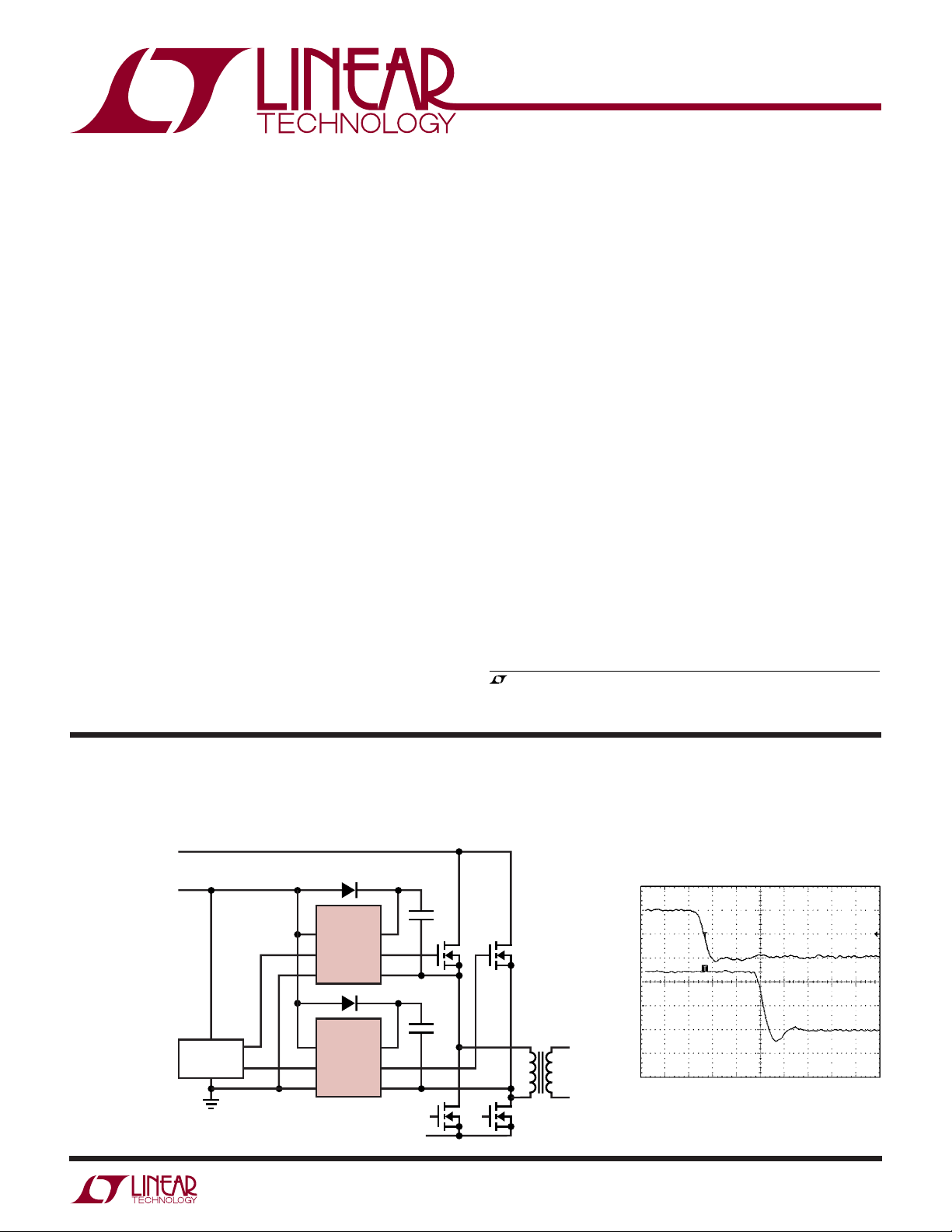
TYPICAL APPLICATIO
Synchronous Phase-Modulated Full-Bridge Converter
V
IN
100V PEAK TRANSIENT
36V TO 72V
(ABS MAX)
V
8V TO 15V
CC
V
CC
LTC3722-1
U
LTC4440
V
CC
INP
GND
LTC4440
V
CC
INP
GND
BOOST
BOOST
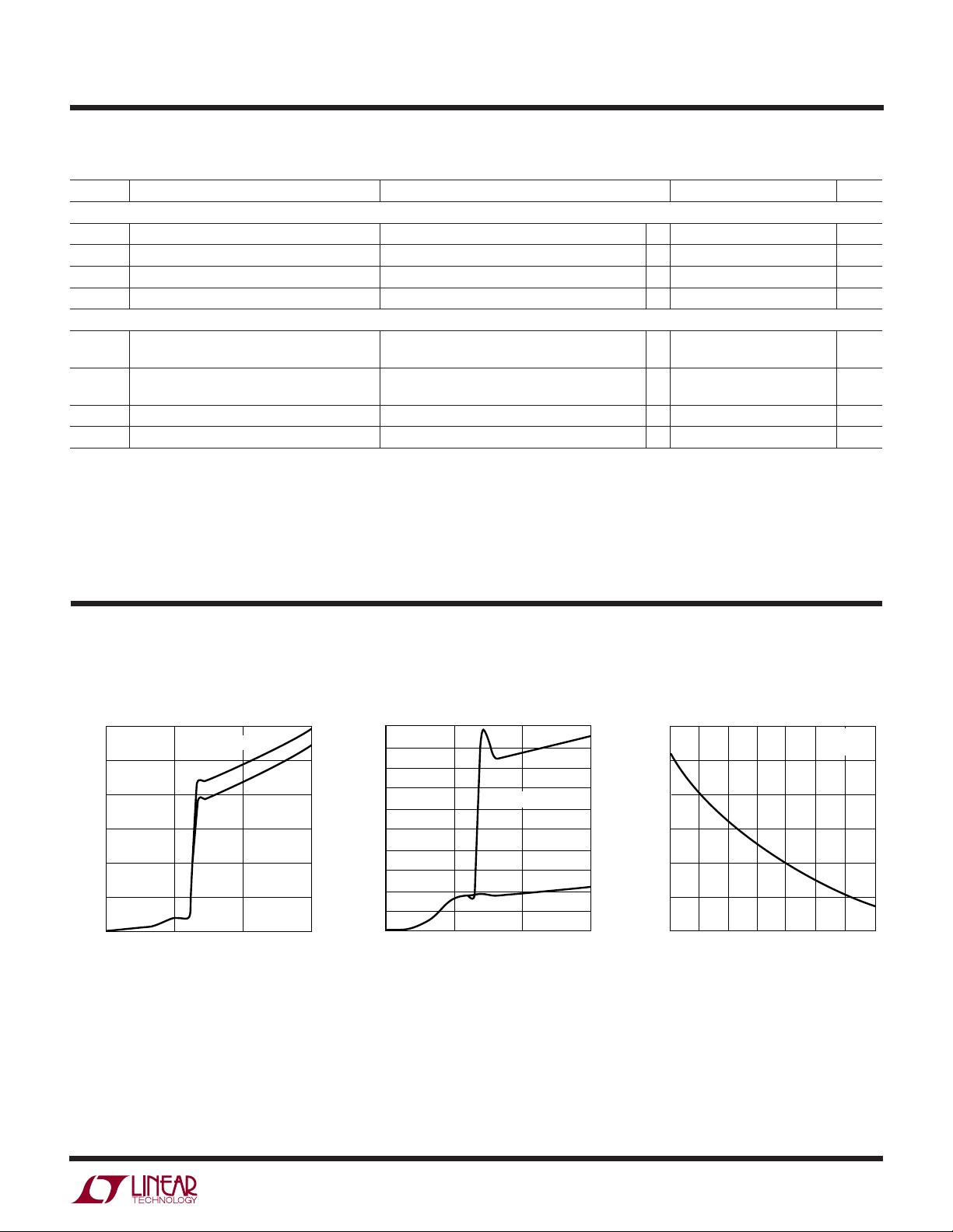
LTC4440 Driving a 1000pF
Capacitive Load
INPUT
(INP)
TG
TS
••
TG
TS
4440 TA01
2V/DIV
OUTPUT
(TG – TS)
5V/DIV
10ns/DIV 4440 F02
4440f
1
LTC4440
1
2
3
4
INP
GND
V
CC
GND
8
7
6
5
TS
TG
BOOST
NC
TOP VIEW
9
MS8E PACKAGE
8-LEAD PLASTIC MSOP
WW
W
ABSOLUTE MAXIMUM RATINGS
U
(Note 1)
Supply Voltage
VCC....................................................... –0.3V to 15V
BOOST – TS ......................................... –0.3V to 15V
INP Voltage............................................... –0.3V to 15V
BOOST Voltage (Continuous) ................... – 0.3V to 95V
BOOST Voltage (100ms) ........................ – 0.3V to 115V
TS Voltage (Continuous) ............................. – 5V to 80V
TS Voltage (100ms)................................... –5V to 100V
U
W
PACKAGE/ORDER INFORMATION
ORDER PART
NUMBER
LTC4440EMS8E
MS8E
T
= 125°C, θJA = 40°C/W (NOTE 4)
JMAX
EXPOSED PAD IS GND (PIN 9)
MUST BE SOLDERED TO PCB
PART MARKING
LTF9
Peak Output Current < 1µs (TG) ............................... 4A
Driver Output TG (with Respect to TS) ..... –0.3V to 15V
Operating Ambient Temperature Range
(Note 2) .............................................. – 40°C to 85°C
Junction Temperature (Note 3)............................ 125°C
Storage Temperature Range ................. –65°C to 150°C
Lead Temperature (Soldering, 10 sec).................. 300°C
U
ORDER PART
TOP VIEW
VCC 1
GND 2
INP 3
S6 PACKAGE
6-LEAD PLASTIC SOT-23
T
= 125°C, θJA = 230°C/W
JMAX
6 BOOST
5 TG
4 TS
NUMBER
LTC4440ES6
PART MARKING
LTZY
S6
Consult LTC Marketing for parts specified with wider operating temperature ranges.
ELECTRICAL CHARACTERISTICS
The ● denotes specifications which apply over the full operating
temperature range, otherwise specifications are at TA = 25°C. VCC = V
SYMBOL PARAMETER CONDITIONS MIN TYP MAX UNITS
Main Supply (VCC)
I
VCC
UVLO Undervoltage Lockout Threshold VCC Rising ● 5.7 6.5 7.3 V
Bootstrapped Supply (BOOST – TS)
I
BOOST
UVLO
Input Signal (INP)
V
IH
V
IL
VIH – VILInput Voltage Hysteresis 0.350 V
I
INP
2
DC Supply Current
Normal Operation INP = 0V 250 400 µA
UVLO V
DC Supply Current
Normal Operation INP = 0V 110 180 µA
UVLO V
Undervoltage Lockout Threshold V
HS
High Input Threshold INP Ramping High ● 1.3 1.6 2 V
Low Input Threshold INP Ramping Low ● 0.85 1.25 1.6 V
Input Pin Bias Current ±0.01 ±2 µA
< UVLO Threshold (Falling) – 0.1V 25 80 µA
CC
Falling ● 5.4 6.2 7.0 V
V
CC
Hysteresis 300 mV
– VTS < UVLO
BOOST
– VTS Rising ● 6.75 7.4 7.95 V
BOOST
– VTS Falling ● 6.25 6.9 7.60 V
V
BOOST
Hysteresis 500 mV
HS(FALLING)
= 12V, VTS = GND = 0V, unless otherwise noted.
BOOST
– 0.1V, VCC = INP = 5V 86 170 µA
4440f
LTC4440
BOOST – TS SUPPLY VOLTAGE (V)
8
OUTPUT (TG – TS) VOLTAGE (mV)
150
155
160
165
170
11 13
4440 G03
145
140
910
12 14 15
ITG = 100mA
T
A
= 25°C
ELECTRICAL CHARACTERISTICS
temperature range, otherwise specifications are at T
The ● denotes specifications which apply over the full operating
= 25°C. VCC = V
A
= 12V, VTS = GND = 0V, unless otherwise noted.
BOOST
SYMBOL PARAMETER CONDITIONS MIN TYP MAX UNITS
Output Gate Driver (TG)
V
OH
V
OL
I
PU
R
DS
High Output Voltage ITG = –10mA, VOH = V
BOOST
– V
TG
0.7 V
Low Output Voltage ITG = 100mA ● 150 220 mV
Peak Pull-Up Current ● 1.7 2.4 A
Output Pull-Down Resistance ● 1.5 2.2 Ω
Switching Timing
t
r
Output Rise Time 10% – 90%, CL = 1nF 10 ns
10% – 90%, CL = 10nF 100 ns
t
f
t
PLH
t
PHL
Note 1: Absolute Maximum Ratings are those values beyond which the life
of a device may be impaired.
Note 2: The LTC4440 is guaranteed to meet performance specifications
from 0°C to 70°C. Specifications over the –40°C to 85°C operating
temperature range are assured by design, characterization and correlation
Output Fall Time 10% – 90%, CL = 1nF 7 ns
10% – 90%, C
= 10nF 70 ns
L
Output Low-High Propagation Delay ● 30 65 ns
Output High-Low Propagation Delay ● 28 65 ns
Note 3: T
is calculated from the ambient temperature TA and power
J
dissipation PD according to the following formula:
= TA + (PD • θJA°C/W)
T
J
Note 4: Failure to solder the exposed back side of the MS8E package to
the PC board will result in a thermal resistance much higher than 40°C/W.
with statistical process controls.
UW
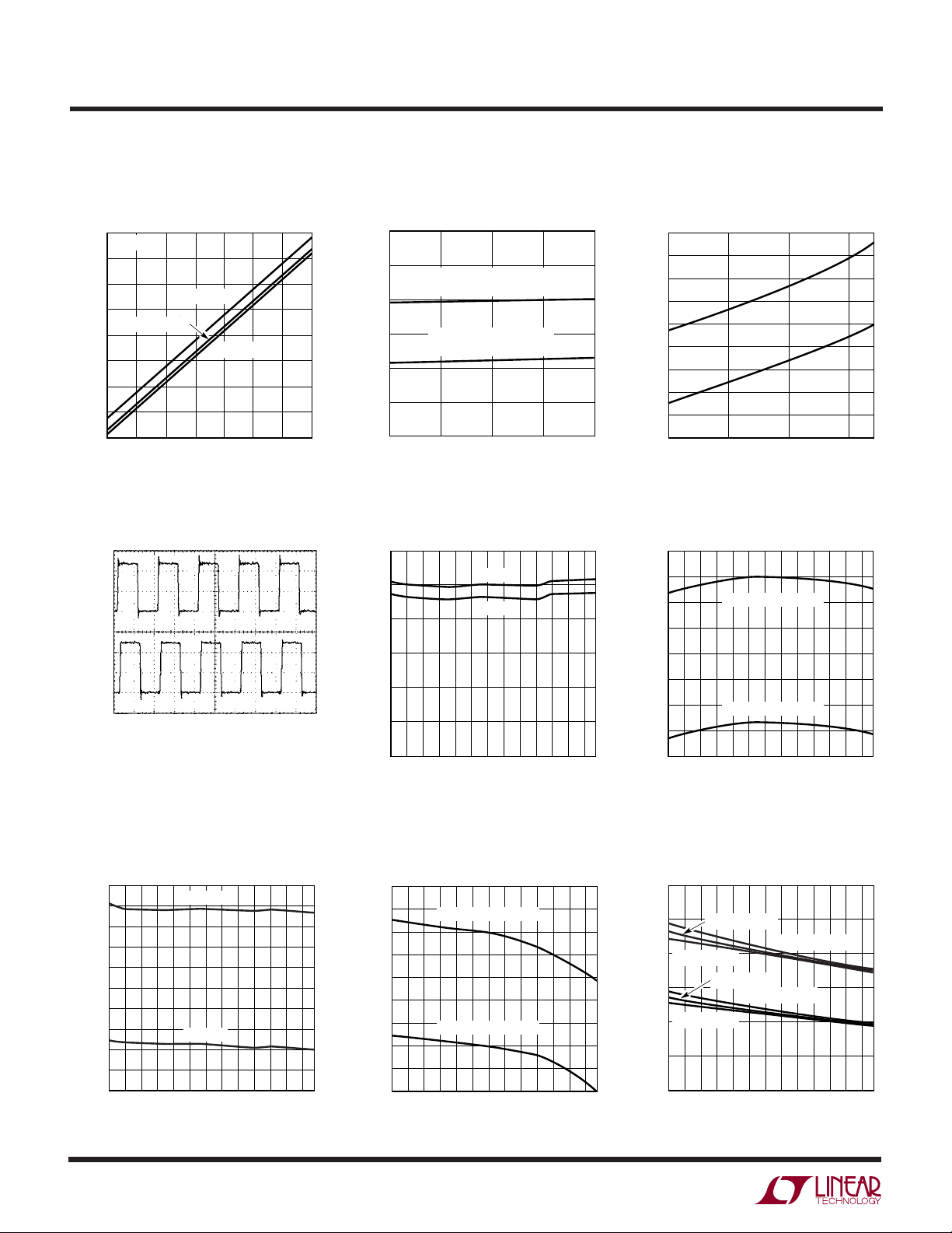
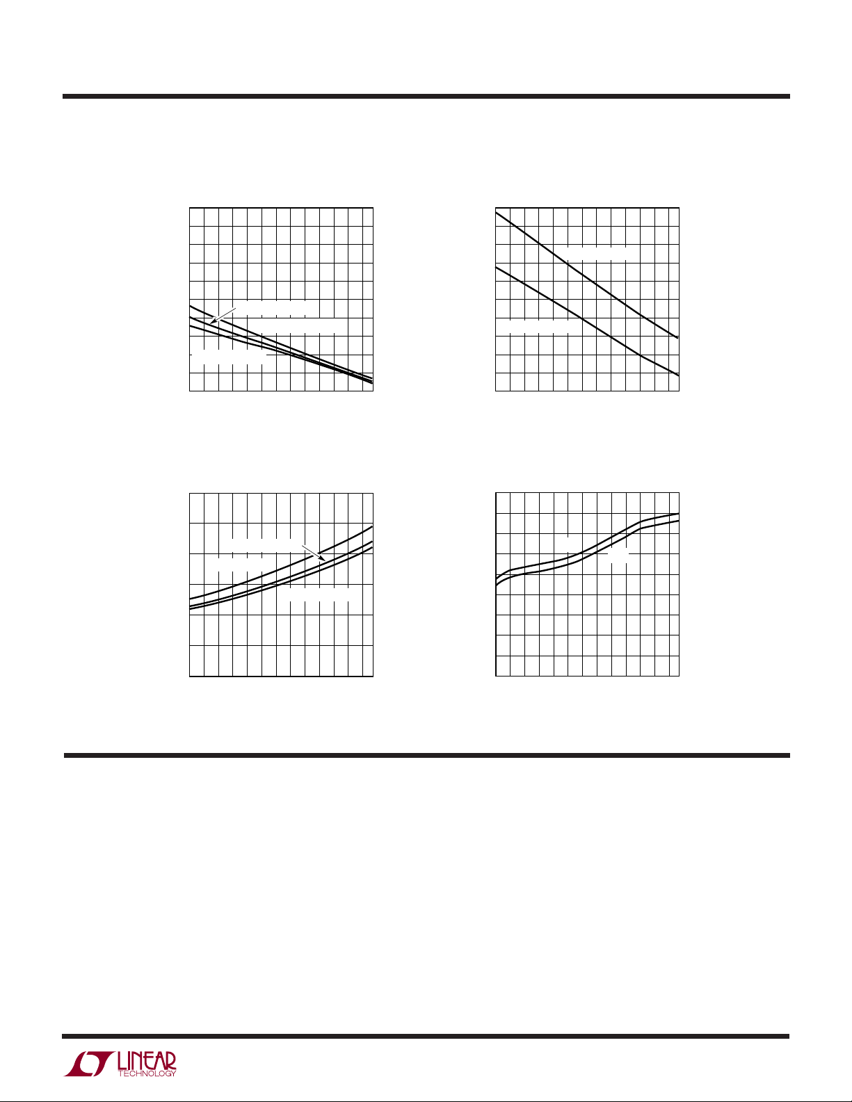
TYPICAL PERFOR A CE CHARACTERISTICS
V
300
250
200
150
100
QUIESCENT CURRENT (µA)
50
0
Supply Quiescent Current
CC
vs Voltage
TA = 25°C
0
510
VCC SUPPLY VOLTAGE (V)
INP = 0V
INP = V
CC
15
4440 G01
BOOST – TS Supply Quiescent
Current vs Voltage
500
TA = 25°C
450
400
350
300
250
200
150
QUIESCENT CURRENT (µA)
100
50
0
0
5
BOOST – TS SUPPLY VOLTAGE (V)
INP = V
INP = 0V
Output Low Voltage (VOL)
vs Supply Voltage
CC
10
15
4440 G02
4440f
3
LTC4440
TEMPERATURE (°C)
–60
INPUT THRESHOLD (V)
1.6
1.8
2.0
12090
4440 G12
1.4
1.2
0.8
–30
30060
1.0
VIH (VCC = 15V)
VIL (VCC = 15V)
VIH (VCC = 8V)
VIL (VCC = 8V)
VIH (VCC = 12V)
VIL (VCC = 12V)
UW
TYPICAL PERFOR A CE CHARACTERISTICS
Output High Voltage (VOH)
vs Supply Voltage
15
TA = 25°C
14
13
12
ITG = –10mA
11
10
9
OUTPUT VOLTAGE (TG – TS) (V)
8
7
910 12
8
BOOST – TS SUPPLY VOLTAGE (V)
ITG = –1mA
11
2MHz Operation
INPUT
(INP)
5V/DIV
OUTPUT
(TG)
5V/DIV
V
= 12V 250ns/DIV 4440 G07
CC
ITG = –100mA
13 14 15
4440 G04
Input Thresholds (INP)
vs Supply Voltage
2.0
TA = 25°C
1.8
1.6
1.4
1.2
INPUT THRESHOLD (V)
1.0
0.8
(INPUT HIGH THRESHOLD)
(INPUT LOW THRESHOLD)
7
9111315
VCC SUPPLY VOLTAGE (V)
V
IH
V
IL
VCC Supply Current (VCC = 12V)
vs Temperature
300
250
200
150
CURRENT (µA)
100
50
0
–60
–30
INP = 0V
INP = 12V
30060
TEMPERATURE (°C)
4440 G05
12090
4440 G08
VCC Supply Current
at TTL Input Levels
380
TA = 25°C
360
340
320
300
280
260
240
SUPPLY QUIESCENT CURRENT (µA)
CC
220
V
200
8
INP = 2V
INP = 0.8V
10
VCC SUPPLY VOLTAGE (V)
VCC Undervoltage Lockout
Thresholds vs Temperature
6.55
6.50
6.45
6.40
6.35
6.30
SUPPLY VOLTAGE (V)
CC
6.25
V
6.20
6.15
–60
RISING THRESHOLD
FALLING THRESHOLD
–30
TEMPERATURE (°C)
30060
12
14
4440 G06
12090
4440 G09
Boost Supply Current
vs Temperature
500
450
400
350
4
300
250
200
CURRENT (µA)
150
100
50
0
–60
INP = 12V
–30
TEMPERATURE (°C)
INP = 0V
30060
12090
4440 G10
Boost Supply (BOOST – TS)
Undervoltage Lockout Thresholds
vs Temperature Input Threshold vs Temperature
7.6
7.5
7.4
7.3
7.2
7.1
7.0
6.9
BOOST – TS SUPPLY VOLTAGE (V)
6.8
6.7
–60
RISING THRESHOLD
FALLING THRESHOLD
–30
TEMPERATURE (°C)
30060
4440 G11
12090
4440f
UW
TYPICAL PERFOR A CE CHARACTERISTICS
LTC4440
Input Threshold Hysteresis
vs Temperature
500
480
460
440
420
400
380
HYSTERESIS (mV)
360
340
VIH-VIL (VCC = 8V)
320
300
–60
VIH-VIL (VCC = 12V)
–30
TEMPERATURE (°C)
VIH-VIL (VCC = 15V)
30060
Output Driver Pull-Down
Resistance vs Temperature
3.0
2.5
2.0
(Ω)
1.5
DS
R
1.0
0.5
0
–60
BOOST – TS = 12V
BOOST – TS = 8V
–30
TEMPERATURE (°C)
BOOST – TS = 15V
30060
12090
4440 G13
12090
4440 G15
Peak Driver (TG) Pull-Up Current
vs Temperature
3.0
2.9
2.8
2.7
2.6
2.5
2.4
BOOST – TS = 12V
PEAK CURRENT (A)
2.3
2.2
2.1
2.0
–60
–30
BOOST – TS = 15V
30060
TEMPERATURE (°C)
Propagation Delay vs Temperature
(VCC = BOOST = 12V)
45
40
35
30
25
20
15
PROPAGATION DELAY (ns)
10
5
0
–60
–30
TEMPERATURE (°C)
t
PLH
t
PHL
30060
12090
4440 G14
12090
4440 G16
U
UU
PI FU CTIO S
SOT-23 Package
VCC (Pin 1): Chip Supply. This pin powers the internal low
side circuitry. A low ESR ceramic bypass capacitor should
be tied between this pin and the GND pin (Pin 2).
GND (Pin 2): Chip Ground.
INP (Pin 3): Input Signal. TTL/CMOS compatible input
referenced to GND (Pin 2).
TS (Pin 4): Top (High Side) Source Connection.
TG (Pin 5): High Current Gate Driver Output (Top Gate).
This pin swings between TS and BOOST.
BOOST (Pin 6): High Side Bootstrapped Supply. An external capacitor should be tied between this pin and TS
(Pin 4). Normally, a bootstrap diode is connected between
VCC (Pin 1) and this pin. Voltage swing at this pin is from
VCC – VD to VIN + VCC – VD, where VD is the forward voltage
drop of the bootstrap diode.
4440f
5

LTC4440
U
UU
PI FU CTIO S
Exposed Pad MS8E Package
INP (Pin 1): Input Signal. TTL/CMOS compatible input
referenced to GND (Pin 2).
GND (Pins 2, 4): Chip Ground.
V
(Pin 3): Chip Supply. This pin powers the internal low
CC
side circuitry. A low ESR ceramic bypass capacitor should
be tied between this pin and the GND pin (Pin 2).
NC (Pin 5): No Connect. No connection required. For
convenience, this pin may be tied to Pin 6 (BOOST) on the
application board.
W
BLOCK DIAGRA
BOOST (Pin 6): High Side Bootstrapped Supply. An external capacitor should be tied between this pin and TS
(Pin 8). Normally, a bootstrap diode is connected between
(Pin 3) and this pin. Voltage swing at this pin is from
V
CC
V
– VD to VIN + VCC – VD, where VD is the forward voltage
CC
drop of the bootstrap diode.
TG (Pin 7): High Current Gate Driver Output (Top Gate).
This pin swings between TS and BOOST.
TS (Pin 8): Top (High Side) Source Connection.
Exposed Pad (Pin 9): Ground. Must be electrically con-
nected to Pins 2 and 4 and soldered to PCB ground for
optimum thermal performance.
8V TO 15V
UWW
TI I G DIAGRA
V
CC
UNDERVOLTAGE
GND
INP
OUTPUT (TG)
LOCKOUT
INPUT (INP)
HIGH SIDE
UNDERVOLTAGE
LOCKOUT
LEVEL SHIFTER
GND
INPUT RISE/FALL TIME <10ns
V
IH
t
r
t
PLH
BOOST
t
PHL
V
IN
UP TO 80V,
BOOST
TG
TS
TS
V
IL
90%
10%
t
f
4440 TD
TRANSIENT
UP TO 100V
4440 BD
6
4440f
WUUU
APPLICATIO S I FOR ATIO
Overview
The LTC4440 receives a ground-referenced, low voltage
digital input signal to drive a high side N-channel power
MOSFET whose drain can float up to 100V above ground,
eliminating the need for a transformer between the low
voltage control signal and the high side gate driver. The
LTC4440 normally operates in applications with input
supply voltages (VIN) up to 80V, but is able to withstand
and continue to function during 100V, 100ms transients
on the input supply.
The powerful output driver of the LTC4440 reduces the
switching losses of the power MOSFET, which increase
with transition time. The LTC4440 is capable of driving a
1nF load with 10ns rise and 7ns fall times using a
bootstrapped supply voltage V
BOOST–TS
Input Stage
The LTC4440 employs TTL/CMOS compatible input thresholds that allow a low voltage digital signal to drive standard
power MOSFETs. The LTC4440 contains an internal voltage regulator that biases the input buffer, allowing the input
thresholds (VIH = 1.6V, VIL = 1.25V) to be independent of
variations in VCC. The 350mV hysteresis between VIH and
VIL eliminates false triggering due to noise during switching transitions. However, care should be taken to keep this
pin from any noise pickup, especially in high frequency, high
voltage applications. The LTC4440 input buffer has a high
input impedance and draws negligible input current, simplifying the drive circuitry required for the input.
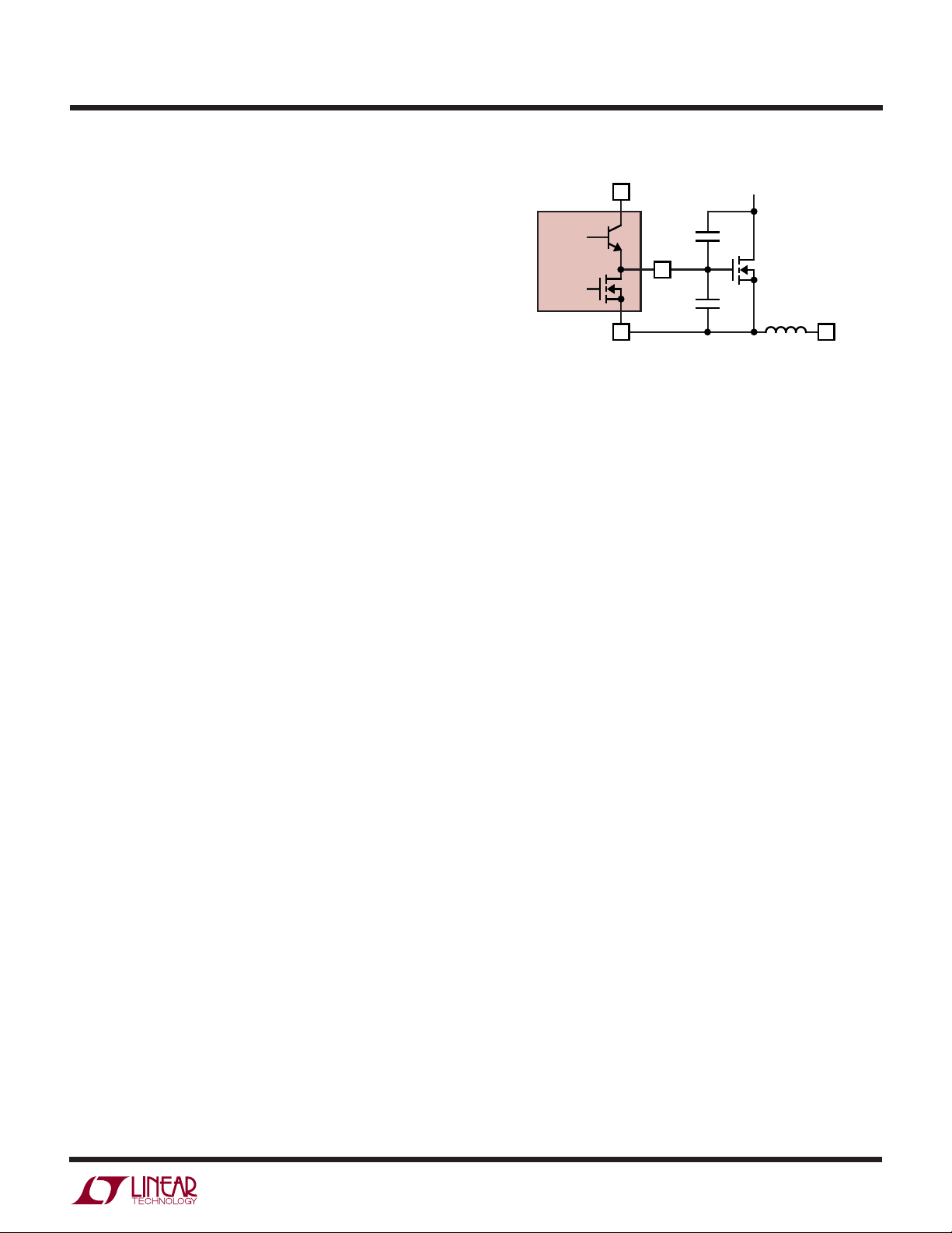
Output Stage
A simplified version of the LTC4440’s output stage is
shown in Figure 3 . The pull-down device is an N-channel
MOSFET (N1) and the pull-up device is an NPN bipolar
junction transistor (Q1). The output swings from the lower
rail (TS) to within an NPN VBE (~0.7V) of the positive rail
(BOOST). This large voltage swing is important in driving
external power MOSFETs, whose R
proportional to its gate overdrive voltage (VGS – VTH).
The LTC4440’s peak pull-up (Q1) current is 2.4A while the
pull-down (N1) resistance is 1.5Ω. The low impedance of
N1 is required to discharge the power MOSFET’s gate
capacitance during high-to-low signal transitions. When
of 12V.
DS(ON)
is inversely
LTC4440
BOOST
LTC4440
Q1
TG
N1
TS
Figure 3. Capacitance Seen by TG During Switching
the power MOSFET’s gate is pulled low (gate shorted to
source through N1) by the LTC4440, its source (TS) is
pulled low by its load (e.g., an inductor or resistor). The
slew rate of the source/gate voltage causes current to flow
back to the MOSFET’s gate through the gate-to-drain
capacitance (CGD). If the MOSFET driver does not have
sufficient sink current capability (low output impedance),
the current through the power MOSFET’s CGD can momentarily pull the gate high, turning the MOSFET back on.
A similar scenario exists when the LTC4440 is used to
drive a low side MOSFET. When the low side power
MOSFET’s gate is pulled low by the LTC4440, its drain
voltage is pulled high by its load (e.g., inductor or resistor). The slew rate of the drain voltage causes current to
flow back to the MOSFET’s gate through its gate-to-drain
capacitance. If the MOSFET driver does not have sufficient
sink current capability (low output impedance), the current through the power MOSFET’s CGD can momentarily
pull the gate high, turning the MOSFET back on.
Rise/Fall Time
Since the power MOSFET generally accounts for the
majority of the power loss in a converter, it is important to
quickly turn it on or off, thereby minimizing the transition
time in its linear region. The LTC4440 can drive a 1nF load
with a 10ns rise time and 7ns fall time.
The LTC4440’s rise and fall times are determined by the
peak current capabilities of Q1 and N1. The predriver that
drives Q1 and N1 uses a nonoverlapping transition scheme
to minimize cross-conduction currents. N1 is fully turned
off before Q1 is turned on and vice versa.
V
IN
UP TO 100V
C
GD
C
GS
POWER
MOSFET
LOAD
INDUCTOR
4440 F03
–
V
4440f
7

LTC4440
WUUU
APPLICATIO S I FOR ATIO
Power Dissipation
To ensure proper operation and long-term reliability, the
LTC4440 must not operate beyond its maximum temperature rating. Package junction temperature can be calculated by:
TJ = TA + PD (θJA)
where:
TJ = Junction Temperature
= Ambient Temperature
T
A
PD = Power Dissipation
θ
= Junction-to-Ambient Thermal Resistance
JA
Power dissipation consists of standby and switching
power losses:
PD = P
STDBY
+ P
AC
where:
P
= Standby Power Losses
STDBY
PAC = AC Switching Losses
The LTC4440 consumes very little current during standby.
The DC power loss at VCC = 12V and V
BOOST–TS
= 12V is
only (250µA + 110µA)(12V) = 4.32mW.
AC switching losses are made up of the output capacitive
load losses and the transition state losses. The capacitive
load losses are primarily due to the large AC currents
needed to charge and discharge the load capacitance
during switching. Load losses for the output driver driving
a pure capacitive load C
Load Capacitive Power = (C
would be:
OUT
OUT
)(f)(V
BOOST–TS
2
)
The power MOSFET’s gate capacitance seen by the driver
output varies with its VGS voltage level during switching.
A power MOSFET’s capacitive load power dissipation can
be calculated using its gate charge, QG. The QG value
corresponding to the MOSFET’s VGS value (VCC in this
case) can be readily obtained from the manufacturer’s Q
G
vs VGS curves:
Load Capacitive Power (MOS) = (V
BOOST–TS
)(QG)(f)
Transition state power losses are due to both AC currents
required to charge and discharge the driver’s internal
nodal capacitances and cross-conduction currents in the
internal gates.
Undervoltage Lockout (UVLO)
The LTC4440 contains both low side and high side undervoltage lockout detectors that monitor V
bootstrapped supply V
BOOST–TS
. When VCC falls below
and the
CC
6.2V, the internal buffer is disabled and the output pin OUT
is pulled down to TS. When V
BOOST – TS
falls below 6.9V,
OUT is pulled down to TS. When both supplies are undervoltage, OUT is pulled low to TS and the chip enters a low
current mode, drawing approximately 25µA from VCC and
86µA from BOOST.
Bypassing and Grounding
The LTC4440 requires proper bypassing on the V
V
BOOST–TS
supplies due to its high speed switching (nano-
CC
and
seconds) and large AC currents (Amperes). Careless
component placement and PCB trace routing may cause
excessive ringing and under/overshoot.
To obtain the optimum performance from the LTC4440:
A. Mount the bypass capacitors as close as possible
between the VCC and GND pins and the BOOST and TS
pins. The leads should be shortened as much as possible to reduce lead inductance.
B. Use a low inductance, low impedance ground plane to
reduce any ground drop and stray capacitance. Remember that the LTC4440 switches >2A peak currents and
any significant ground drop will degrade signal integrity.
C. Plan the power/ground routing carefully. Know where
the large load switching current is coming from and
going to. Maintain separate ground return paths for the
input pin and the output power stage.
D. Keep the copper trace between the driver output pin and
the load short and wide.
E. When using the MS8E package, be sure to solder the
exposed pad on the back side of the LTC4440 package
to the board. Correctly soldered to a 2500mm2 doublesided 1oz copper board, the LTC4440 has a thermal
resistance of approximately 40°C/W. Failure to make
good thermal contact between the exposed back side
and the copper board will result in thermal resistances
far greater than 40°C/W.
4440f
8

TYPICAL APPLICATIO S
18
10
911
12V
V
IN
12
LTC3722EGN-1
PDLY
OUTF
OUTE
COMPSSPGNDGND
CS
V
IN
SBUS
UVLO
1µF
ADLY
330pF
MMBT3904
2.2nF
100k
D12
5.1V
T3
1(1.5mH):0.5
T1
5(105µH):1:1
T2
5:5(105µH):1:1
2.49k
9.53k
10k
2.7k
470Ω
1/4W
L4
1mH
C3
68µF
20V
V
H
•
•
16
15
8
19
5
4
150Ω
0.02Ω
1.5W
30.1k
220pF
100Ω
330Ω
1.10k
909Ω
4.87k
1/4W
4.87k
1/4W
51Ω
2W
220pF
182k
20k
1/4W
220pF
4.99k
20k
180pF
68nF
220pF0.47µF
150k
SYNC PV
CC
CSE
+
LTC3901EGN
CSE
–
8
65
1
41013 7
1µF
1µF
4440 TA03
–V
OUT
V
OUT
–V
OUT
D10
10V
V
OUT
ME ME2
GND PGND GND2 PGND2 TIMER
V
CC
330pF
23
1.10k
909Ω
39.2k
100Ω
1k
CSF
+
–V
OUT
V
OUT
V
OUT
–V
OUT
V
OUT
12V/35A
–V
OUT
CSF
–
11 12
MF MF2
14 15 16
22nF
Si7852DP
×4
Si7852DP
×4
Si7852DP
×2
L1
1.3µH
114
2
12V
D7
D8
4
2
1
6
•
••••
••
•
10
8
7
+
1
0.22µF
Si7852DP
×2
3
6
7
824
A
D2
LTC4440EMS8E
BOOSTINP
TG
TSGNDGND
V
CC
12V
1
0.22µF
Si7852DP
×2
3
6
7
8
12VD
24
C
D3
D4
D5
51Ω
2W
0.47µF
100V
LTC4440EMS8E
BOOSTINP
TG
TSGNDGND
V
CC
12V
1µF
100V
×4
V
IN
V
IN
–V
IN
36V TO 72V
1µF
100V
17
D
OUTD
19
10Ω
10Ω
C
OUTC
20
B
OUTB
21
A
OUTA
C1, C2
180µF
16V
×2
+
1µF
0.47µF, 100V TDK C3216X7R2A474M
1µF, 100V TDK C4532X7R2A105M
C1,C2: SANYO 16SP180M
C3: AVX TPSE686M020R0150
C4: MURATA DE2E3KH222MB3B
D1, D4-D6: MURS120T3
D2, D3, D7, D8: BAS21
D9: MMBZ5226B
D10: MMBZ5240B
D11: BAT54
D12: MMBZ231B
L1: SUMIDA CDEP105-1R3MC-50
L2: PULSE PA0651
L3: PA1294.910
L4: COILCRAFT DO1608C-105
Q1, Q2: ZETEX FMMT619
Q3, Q4: ZETEX FMMT718
T1, T2: PULSE PA0526
T3: PULSE PA0785
6
3
422236
33k
57
D11
8.25k
I
SNS
5V
REF
I
SNS
0.1µF
58
1
2
1
MOC207
C4
2.2nF
250V
0.047µF
3
6
5
8
GND-F
V
+
GND-S
COLL REF
LT1431CS8
1.1k
22Ω
200k
750Ω
100Ω
D9 3.3V
0.02Ω
1.5W
V
H
D1
D6
13k
1/2W
0.47µF
100V
820pF
200V
L3
0.85µH
15Ω
1W
0.47µF
100V
Si7852DP
×2
12VB
Q1
Q3
Q2
Q4
11
10
8
7
MMBT3904
FBSPRG
R
LEB
10k
13
SYNC
5.1k
1
NC
8
DPRG
2
V
REF
5V
REF
14
C
T
24
L2
150nH
•
LTC4440
U
to 12V/35A Isolated Full-Bridge Supply
IN
LTC3722/LTC4440 420W 36V-72V
4440f
9

LTC4440
5
46
A
B
12V
V
IN
15
LTC3723EGN-1
DRVB
SDRB
SDRA
COMP
CS
V
CC
UVLO
9
150k
1
0.47µF
1µF
DRVA
DPRG V
REF
SPRGGND SSFB C
T
330pF
22nF
100k
D8
10V
68nF
270pF
T2
1(1.5mH):0.5
T1
4T:6T(65µHMIN):6T:2T:2T
243k
2.49k
9.53k
10k
750Ω
1k
100Ω
1/4W
813
3
Si7370DP
×2
L4
1mH
C3
68µF
20V
V
F
D2
•
•
3
2
8
19
5
4
16
10k
33k
200Ω
1/4W
R1
0.03Ω
1.5W
66.5k
RLEB
12
7
14
220pF
22nF
100Ω
665Ω
1k
866Ω
6.19k
1/4W
1.5nF
464k
30k
1/4W
SYNC PV
CC
CSF
+
V
F
LTC3901EGN
CSF
–
8
11 12
1
41013 7
22nF
1µF
4.7µF
4440 TA05
–V
OUT
V
OUT
–V
OUT
D7
10V
V
OUT
MF MF2
GND PGND GND2 PGND2 TIMER
V
CC
470pF
14 15
1k
866Ω
42.2k
1k
100Ω
6.19k
1/4W
CSE
+
V
E
–V
OUT
V
OUT
V
F
V
OUT
12V/20A
–V
OUT
CSE
–
65
ME ME2
23 16
Si7370DP
×2
Si7852DPSi7852DP
L5
0.56µH
112
4
12V
D5
D6
3
5
1
6
•
••
•
•
9
7
V
E
+
0.1µF
Si7852DP
1
6
5
4
B
2
A
D3
LTC4440ES6
BOOSTINP
TG
TSGND
V
CC
12V
3
0.1µF
Si7852DP
1
6
5
42
B
D4
LTC4440ES6
BOOSTINP
TG
TSGND
V
CC
12V
1µF
100V
×3
V
IN
V
IN
–V
IN
42V TO 56V
1µF
100V
C1, C2
47µF
16V
×2
+
1µF
1µF
100V
1k
1/4W
1µF, 100V TDK C3225X7R2A105M
C1,C2: SANYO 16TQC47M
C3: AVX TPSE686M020R0150
C4: MURATA GHM3045X7R222K-GC
D2: DIODES INC. ES1B
D3-D6: BAS21
D7, D8: MMBZ5240B
L4: COILCRAFT DO1608C-105
L5: COILCRAFT DO1813P-561HC
L6: PULSE PA1294.132 OR
PANASONIC ETQP1H1R0BFA
R1, R2: IRC LRC2512-R03G
T1: PULSE PA0805.004
T2: PULSE PA0785
6
10
I
SNS
I
SNS
0.1µF
11
58
1
2
1
MOC207
C4
2.2nF
250V
0.1µF
3
6
5
8
GND-F
V
+
GND-S
COLL REF
LT1431CS8
A
1.5k
22Ω
4.7Ω
4.7Ω
R2
0.03Ω
1.5W
V
E
470pF
100V
L6
1.25µH
10Ω
1W
6
93
EFFICIENCY (%)
94
95
96
97
81012
LOAD CURRENT (A)
14
16 18 20
42V
IN
48V
IN
56V
IN
MMBT3904
•
TYPICAL APPLICATIO S
U
10
to 12V/20A Isolated 1/4Brick (2.3" × 1.45")
IN
LTC3723-1 240W 42-56V
4440f
PACKAGE DESCRIPTION
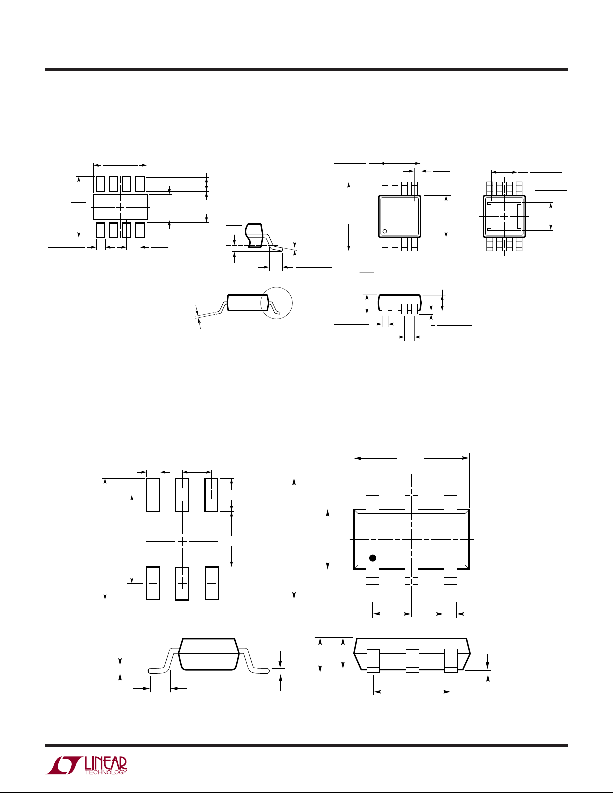
LTC4440
U
MS8E Package
8-Lead Plastic MSOP
(Reference LTC DWG # 05-08-1662)
± 0.102
0.889 ± 0.127
(.035 ± .005)
3.20 – 3.45
(.126 – .136)
GAUGE
PLANE
0.18
(.007)
0.254
(.010)
DETAIL “A”
DETAIL “A”
2.794 ± 0.102
(.110 ± .004)
5.23
(.206)
MIN
0.42 ± 0.038
(.0165 ± .0015)
TYP
RECOMMENDED SOLDER PAD LAYOUT
NOTE:
1. DIMENSIONS IN MILLIMETER/(INCH)
2. DRAWING NOT TO SCALE
3. DIMENSION DOES NOT INCLUDE MOLD FLASH, PROTRUSIONS OR GATE BURRS.
MOLD FLASH, PROTRUSIONS OR GATE BURRS SHALL NOT EXCEED 0.152mm (.006") PER SIDE
4. DIMENSION DOES NOT INCLUDE INTERLEAD FLASH OR PROTRUSIONS.
INTERLEAD FLASH OR PROTRUSIONS SHALL NOT EXCEED 0.152mm (.006") PER SIDE
5. LEAD COPLANARITY (BOTTOM OF LEADS AFTER FORMING) SHALL BE 0.102mm (.004") MAX
2.083
(.082 ± .004)
0.65
(.0256)
BSC
6-Lead Plastic SOT-23
(Reference LTC DWG # 05-08-1636)
° – 6° TYP
0
0.53 ± 0.152
(.021 ± .006)
SEATING
PLANE
S6 Package
3.00 ± 0.102
(.118 ± .004)
(NOTE 3)
4.90
± 0.152
(.193 ± .006)
0.22 – 0.38
(.009 – .015)
TYP
1.10
(.043)
MAX
8
12
0.65
(.0256)
BSC
0.52
7
(.0205)
6
5
REF
3.00 ± 0.102
(.118 ± .004)
(NOTE 4)
4
3
0.86
(.034)
REF
0.127 ± 0.076
(.005 ± .003)
MSOP (MS8E) 0603
1
8
BOTTOM VIEW OF
EXPOSED PAD OPTION
2.06 ± 0.102
(.081 ± .004)
1.83 ± 0.102
(.072 ± .004)
0.62
MAX
3.85 MAX
2.62 REF
RECOMMENDED SOLDER PAD LAYOUT
PER IPC CALCULATOR
0.20 BSC
DATUM ‘A’
NOTE:
1. DIMENSIONS ARE IN MILLIMETERS
2. DRAWING NOT TO SCALE
3. DIMENSIONS ARE INCLUSIVE OF PLATING
0.95
REF
1.22 REF
1.4 MIN
0.30 – 0.50 REF
2.90 BSC
(NOTE 4)
2.80 BSC
0.09 – 0.20
(NOTE 3)
4. DIMENSIONS ARE EXCLUSIVE OF MOLD FLASH AND METAL BURR
5. MOLD FLASH SHALL NOT EXCEED 0.254mm
6. JEDEC PACKAGE REFERENCE IS MO-193
1.50 – 1.75
(NOTE 4)
1.00 MAX
PIN ONE ID
0.95 BSC
0.80 – 0.90
1.90 BSC
0.30 – 0.45
6 PLCS (NOTE 3)
0.01 – 0.10
S6 TSOT-23 0302
4440f
Information furnished by Linear Technology Corporation is believed to be accurate and reliable.
However, no responsibility is assumed for its use. Linear Technology Corporation makes no representation that the interconnection of its circuits as described herein will not infringe on existing patent rights.
11

LTC4440
TYPICAL APPLICATIO
LTC3723-2/LTC4440/LTC3901 240W 42V-56VIN to Unregulated 12V Half-Bridge Converter
30.1k
48V
L1
0.56µH
V
IN
1µF
IN
100V
–V
IN
IN
MMBT3904
15k
1/4W
215k
100pF
12V
MMBZ5242B
1µF
100V
A
120Ω
3
11V12VV
1µF
V
IN
11V
1
V
CC
BOOSTINP
LTC4440ES6
TSGND
5
V
15
UVLO
DPRG V
1µF
330pF
CC
TG
42
DRVA
0.22µF
A
12
62k
D1
6
5
B
46
DRVB
RAMP SPRG GND SSCS FBC
REF
1
150pF
0.47µF
U
1µF
1µF
100V
100V
1µF
10k
7 10 14
100V
68µF
C3
12V
+
SDRB
SDRA
COMP
1k
470pF
Si7852DP
×2
Si7852DP
×2
LTC3723EGN-2
T
8913
16
1µF
100V
1mH
L3
T2
70(980µH):1
+
CS
•
3
2
22Ω
3
11
0.22µF
0.47µF
871
D2
D3
4.7k
V
•
••
72
9
•
•
T3
•
+
CS
7.5Ω
11
Si7370DP
C1
2.2nF
250V
T1
5:4:4:2:2
4
100Ω
5
D4 D5
7.5Ω
V
4
3
•
5
1
6
1(1.5mH):0.5
19
•
0.1µF
8
B
2N7002
E
L2 0.22µH
1500pF
F
×2
V
F
4.7k
1/4W
10k 3k
11 12
+
CSF
SYNC PV
220pF
20Ω 1W
100V
Si7370DP
×2
V
E
4.7k
1/4W
10k 3k
14 15
–
CSF
MF MF2
GND PGND GND2 PGND2 TIMER
1µF, 100V TDK C4532X7R2A105M
C1: MURATA DE2E3KH222MB3B
C2: SANYO 16SP180M
C3: AVX TPSE686M020R0150
D1-D3: BAS21
D4, D5: MMBD914
L1: COILCRAFT DO1813P-561HC
L2: SUMIDA CDEP105-0R2NC-50
L3: COILCRAFT DO1608C-105
T1: PULSE PA0801.005
T2: PULSE P8207
T3: PULSE PA0785
65
+
CSE
CSE
LTC3901EGN
8
41013 7
+
23 16
–
ME ME2
–V
V
OUT
C2
180µF
16V
OUT
V
330pF
CC
CC
V
OUT
1µF
–V
OUT
33.2k 100Ω
1
–V
OUT
1µF
1µF
MMBT3904
4440 TA04
V
OUT
1k
10V
MMBZ5240B
RELATED PARTS
PART NUMBER DESCRIPTION COMMENTS
LTC1155 Dual Micropower High/Low Side Drivers with 4.5V to 18V Supply Range
LT®1161 Quad Protected High Side MOSFET Driver 8V to 48V Supply Range, tON = 200µs, t
LTC1163 Triple 1.8V to 6V High Side MOSFET Driver 1.8V to 6V Supply Range, tON = 95µs, t
LT1339 High Power Synchronous DC/DC Controller Current Mode Operation Up to 60V, Dual N-Channel Synchronous Drive
LTC1535 Isolated RS485 Transceiver 2500V
LTC1693 Family High Speed Dual MOSFET Drivers 1.5A Peak Output Current, 4.5V ≤ VIN ≤ 13.2V
LT3010/LT3010-5 50mA, 3V to 80V Low Dropout Micropower Regulators Low Quiescent Current (30µA), Stable with Small (1µF) Ceramic Capacitor
LT3430 High Voltage, 3A, 200kHz Step-Down Switching Regulator Input Voltages Up to 60V, Internal 0.1Ω Power Switch, Current Mode
LTC3722-1/ Synchronous Dual Mode Phase Modulated Full-Bridge Adaptive Zero Voltage Switching, High Output Power Levels
LTC3722-2 Controllers (Up to Kilowatts)
LTC3723-1/ Synchronous Push-Pull PWM Controllers Current Mode or Voltage Mode Push-Pull Controllers
LTC3723-2
LT3781/LTC1698 36V to 72V Input Isolated DC/DC Converter Chip Set Synchronous Rectification; Overcurrent, Overvoltage, UVLO Protection;
LT3804 Secondary Side Dual Output Controller with Opto Driver Regulates Two Secondary Outputs, Optocoupler Feedback Divider and
LTC3900 Synchronous Rectifier Driver for Forward Converters Programmable Time Out, Reverse Inductor Current Sense
LTC3901 Secondary Side Synchronous Driver for Push-Pull and Programmable Time Out, Reverse Inductor Current Sense
LTC4441 6A MOSFET Driver Adjustable Gate Drive from 5V to 8V, 5V ≤ VIN ≤ 28V
12
Internal Charge Pump
Full-Bridge Converters
Linear Technology Corporation
1630 McCarthy Blvd., Milpitas, CA 95035-7417
(408) 432-1900 ● FAX: (408) 434-0507
●
www.linear.com
= 28µs
OFF
= 45µs
OFF
of Isolation Between Line Transceiver and Logic Level Interface
RMS
Architecture, 16-Pin Exposed Pad TSSOP Package
Power Good Output Signal; Voltage Margining; Compact Solution
Second Output Synchronous Driver Controller
LT/TP 1004 1K • PRINTED IN USA
© LINEAR TECHNOLOGY CORPORATION 2003
4440f
 Loading...