

L DESIGN IDEAS
4358
B530C
CURRENT (A)
VOLTAGE DROP (mV)
5000
6
0
100 200 300 400
1
2
4
3
5
DIODE (B530C)
FET (LTC4358)
CURRENT (A)
0
0
POWER DISSIPATION (W)
0.5
1.0
1.5
2.0
2.5
213 4 5 6
DIODE (B530C)
POWER SAVED
FET (LTC4358)
LTC4358
GND
IN DRAIN
V
DD
OUT
VIN = 12V
V
OUT
TO
5A LOAD
Ideal Diode Betters a Schottky by a
Factor of Four in Power and Space
Consumption
Introduction
High availability systems often use
parallel power supplies or battery
feeds to achieve redundancy and
enhance system reliability. Traditionally, Schottky ORing diodes are used
to connect these supplies at the point
of load and prevent backfeeding into
a faulty power supply. Unfortunately,
the forward voltage drop of these diodes
reduces the available supply voltage
and dissipates significant power at
high currents—costly heat sinks and
elaborate layouts are needed to keep
the diodes cool.
When power dissipation is a
concern, the Schottky diode can be
replaced with a MOSFET-based ideal
diode. This reduces the voltage drop
and power dissipation, thereby reducing the complexity, size and cost of the
thermal layout and increasing system
efficiency. The LTC4355, LTC4357
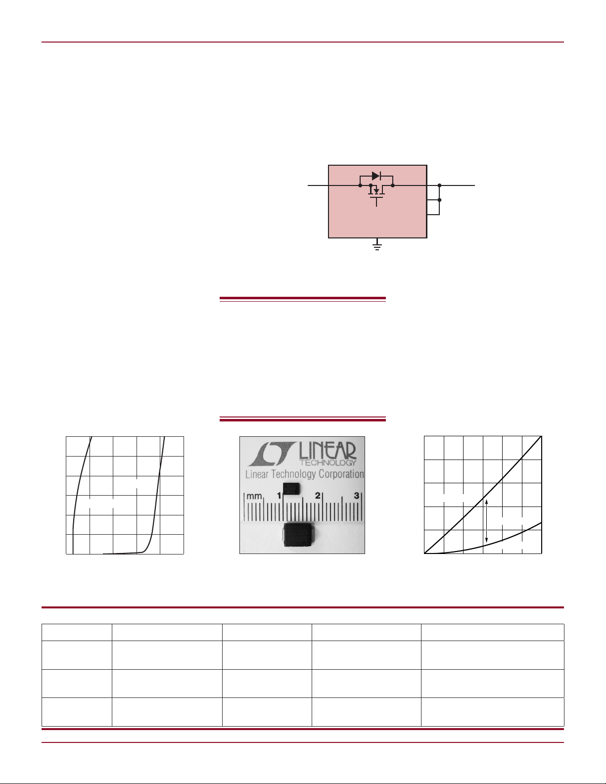
Figure 1. No external components are needed for a 12V/5A ideal diode.
With one-fourth the
dissipated power, system
efficiency is increased and
PCB layout is simplified—no
need for costly and bulky
heat sinks.
by Meilissa Lum
and LTC4358 enable MOSFET-based
ideal diode solutions for various applications—the choice depends on the
current and operating voltage of the
application. Table 1 compares these
devices.
Ideal Diode Easier to Use
Than a Schottky
Of particular interest is the LTC4358,
which includes an internal 20mΩ
Figure 2. The LTC4358 ideal diode takes on a 5A B530C Schottky diode. The LTC4358 easily wins in voltage drop, power loss and package size.
Table 1. Comparison of ideal diode parts
Part Number Description Operating Voltage Configuration Package
LTC4355
LTC4357
LTC4358 Ideal Diode
38
38
Positive Voltage Diode-OR
Controller and Monitor
Single Positive Voltage
Ideal Diode Controller
9V–80V,
100V Abs Max
9V–80V,
100V Abs Max
9V–26.5V,
28V Abs Max
Dual, External MOSFETs DFN14 (4mm × 3mm), SO16
Single, External MOSFET DFN6 (2mm × 3mm), MSOP8
5A Internal MOSFET DFN14 (4mm × 3mm), TSSOP16
Linear Technology Magazine • June 2008
DESIGN IDEAS L
V
IN
GND
V
OU T
DIODE CURRENT (A)
3.5
AREA (INCH
2
)
4.5
10
0.1
1
4.0 6.56.0
5.5
5.0
3.0
85oC 70oC 25oC
TA =
50oC
Authors can be contacted
at (408) 432-1900
MOSFET as the pass element. No external components are required. The
IN pins are the source of the MOSFET
and act like the anode of a diode, while
the drain behaves as the cathode,
as shown for a 12V/5A application
in Figure 1. When power is first applied, the load current initially flows
through the MOSFET’s body diode.
The MOSFET’s gate is enhanced and
turned on to maintain a 25mV forward
voltage drop. If the load current causes
more than 25mV of voltage drop, the
MOSFET is driven fully on, and the
forward drop equals R
DS(ON)
• I
LOAD
. If
the load current reverses, as may occur
during an input short, the LTC4358
responds by turning off the internal
MOSFET in less than 0.5µs.
Power Saved Versus
Schottky Diode
Compared to a B530C Schottky diode in the SMC package, not only is
the LTC4358’s DE14 (4mm × 3mm)
package one-fourth the size, the voltage drop and power dissipation are
also considerably less as shown in
Figure 2. The reduced voltage drop
of the ideal diode also increases the
voltage at the load, which reduces the
capacitance required to hold up the
output during supply disruptions. The
Not only is the LTC4358’s
DE14 (4mm × 3mm) package
one-fourth the size, the
voltage drop and power
dissipation are also
considerably less than
a Schottky. The reduced
voltage drop of the ideal
diode also increases the
voltage at the load, which
reduces the capacitance
required to hold up the
output during supply
disruptions.
power dissipated at 5A in the Schottky
is 2W versus 0.5W for the LTC4358.
With one-fourth the power dissipated,
system efficiency is increased and PCB
Figure 4. Maximum diode current vs PCB area
layout is simplified—no need for costly
and bulky heat sinks.
PCB Layout
As described above, with only onefourth as much power dissipation as
a Schottky, thermal layout with the
LTC4358 is much easier. Most of the
heat escapes the part through the
DRAIN/exposed pad, while some exits
through the IN pins. Maximizing the
copper of these connections increases
the allowable maximum current.
Figure 3 shows an optimal layout for
a 1" × 1" single sided PCB with the
DFN package. Copper connected to
the exposed pad above and below the
LTC4358 helps remove heat from the
package. If you are using a two-sided
PCB, use vias under the LTC4358 to
transfer heat to copper on the bottom of the PCB, thus increasing the
maximum current by 10%. Use Figure
4 to determine the amount of copper
area needed for a specified current
and ambient temperature.
Linear Technology Magazine • June 2008
Figure 3. DFN layout considerations for 1" × 1" single sided PCB
Conclusion
The LTC4358 is a MOSFET -based
ideal diode that can directly replace
a 5A Schottky diode in 9V to 26.5V
applications. The LTC4358 betters a
Schottky by a factor of four on voltage drop, power loss and package
size, thus significantly shrinking the
thermal layout and improving overall
performance. Also, simple optimization the PCB layout increases the
maximum current—no heat sinks
required.
L
3939
 Loading...