

L DESIGN FEATURES
LOAD CURRENT (A)
0
0
POWER DISSIPATION (W)
2.5
2.0
1.5
1.0
0.5
4.0
3.0
3.5
2
4 6 8 10
DIODE (SBG1025L)
MOSFET (Si7336ADP)
POWER
SAVED
V
CC
UV
OV
REV
LTC4352
STATUS
FAULT
MOSFET ON
STATUS
OPTIONAL
0.1µF
TO LOAD
2.9V TO 18V
Si4438DY
FAULT
0.1µF
CPO V
IN
SOURCE GATE
GND
OUT
VINV
CC
V
CC
UV
OV
0.5V
REV
1V
–
+
LDO
GND
LOGIC
CHARGE
PUMP
OPEN
MOSFET
DETECT
MOSFET
ON
DETECT
STATUS
FAULT
10µA
10µA
100µA
0.1µF
0.1µF
25mV
OUTCPOGATESOURCE
AMP
Si7336ADP
SUPPLY
INPUT
OUTPUT
TO LOAD
V
IN
V
CC
V
CC
+
–
+
–
+
–
+
0V to 18V Ideal Diode Controller
Saves Watts and Space over Schottky
Introduction
Schottky diodes are used in a variety
of ways to implement multisource
power systems. For instance, high
availability electronic systems, such
as network and storage servers, use
power Schottky diode-OR circuits to
realize a redundant power system.
Diode-ORing is also used in systems
that have alternate power sources,
such as an AC wall adapter and a
backup battery feed. Power diodes
can be combined with capacitors to
hold up a load voltage during an input brownout. In this case, the power
diodes are placed in series with the
input voltage, with the capacitors on
the load side of the diode. While the
capacitors provide power, the reversebiased diode isolates the load from the
sagging input.
Schottky diodes suffice for these
applications when currents are below
a few amperes, but for higher currents, the excess power dissipated in
the diode due to its forward voltage
drop demands a better solution. For
instance, 5A flowing through a diode
with a 0.5V drop wastes 2.5W within
the diode. This heat must be dissipated
with dedicated copper area on the
PCB or heat sinks bolted to the diode,
both of which take significant space.
The diode’s forward drop also makes
by Pinkesh Sachdev
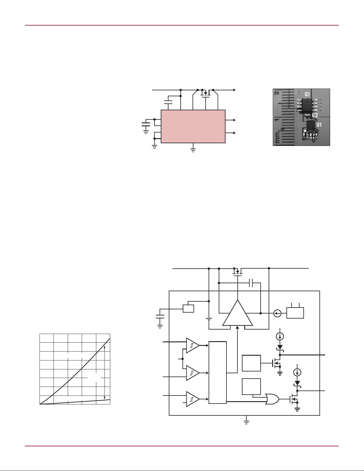
Figure 1. The LTC4352 controlling an N-Channel MOSFET replaces a power diode and associated
heat sink to save power, PCB area, and voltage drop. Also shown: the small PCB footprint of the
ideal diode circuit using a 3mm × 3mm DFN-12 packaged LTC4352 and SO-8 size MOSFET.
it impractical for low voltage applications. This problem calls out for an
ideal diode with a zero forward voltage
drop to save power and space.
The LTC4352 ideal diode controller
in tandem with an N-channel MOSFET
creates a near -ideal diode for use with
0V to 18V input supplies. Figure 1 illustrates the simplicity of this solution.
This ideal diode circuit can replace a
power Schottky diode to create a highly
efficient power ORing or supply holdup
application. Figure 2 shows the power
savings of the ideal diode circuit over
a Schottky diode. 3.5W is saved at
10A, and the saving increases with
load current. With its fast dynamic
response, the controller excels in low
voltage diode-OR applications which
are more sensitive to voltage droop.
Figure 2. As load current increases, so do the
power savings gained from using an ideal diode
(LTC4352 + Si7336ADP) instead of a power
Schottky diode (SBG1025L).
24
Figure 3. Simplified internals of the LTC4352
Linear Technology Magazine • September 2008
DESIGN FEATURES L
FORWARD VOLTAGE (V)
0.025
0
CURRENT (A)
CONSTANT
R
DS(ON)
0.5
CONSTANT
VOLTAGE
SCHOTTKY
DIODE
LTC4352
25mV
R
DS(ON)
TIME (5µs/DIV)
V
IN1
V
LOAD
V
IN1
V
IN2
V
IN2
VOLTAGE
(2V/DIV)
V
CC
UV
OV
REV
LTC4352
STATUS
FAULT
0.1µF
V
IN1
3.5V
Q1
Si4438DY
Q3
Si4438DY
0.1µF
CPO V
IN
SOURCE GATE
GND
OUT
V
CC
UV
OV
REV
LTC4352
STATUS
FAULT
0.1µF
C
L
100µF
V
IN2
3.3V
I
L
8A
0.1µF
CPO V
IN
SOURCE GATE
GND
OUT
TIME (5µs/DIV)
$V
GATE1
$V
GATE
= V
GATE
– V
SOURCE
$V
GATE2
VOLTAGE
(2V/DIV)
What Makes It Ideal?
The LTC4352 monitors the differential
voltage across the MOSFET source
(the “anode”) and drain (the “cathode”)
terminals. The MOSFET has an intrinsic source-to-drain body diode which
conducts the load current at initial
power-up. When the input voltage is
higher than the output, the MOSFET is
turned on, resulting in a forward voltage drop of I
can be suitably chosen to provide an
easy 10x reduction over a Schottky
diode’s voltage drop. When the input
drops below the output, the MOSFET
is turned off, thus emulating the behavior of a reverse biased diode.
An inferior ideal diode control technique monitors the voltage across the
MOSFET with a hysteretic comparator.
For example, the MOSFET could be
turned on whenever the input to output voltage exceeds 25mV. However,
choosing the lower turn-off threshold
can be tricky. Setting it to a positive
forward voltage drop, say 5mV, causes
the MOSFET to be turned off and
on repeatedly at light load currents.
Setting it to a negative value, such as
–5mV, allows DC reverse current.
LOAD
• R
DS(ON)
. The R
DS(ON)
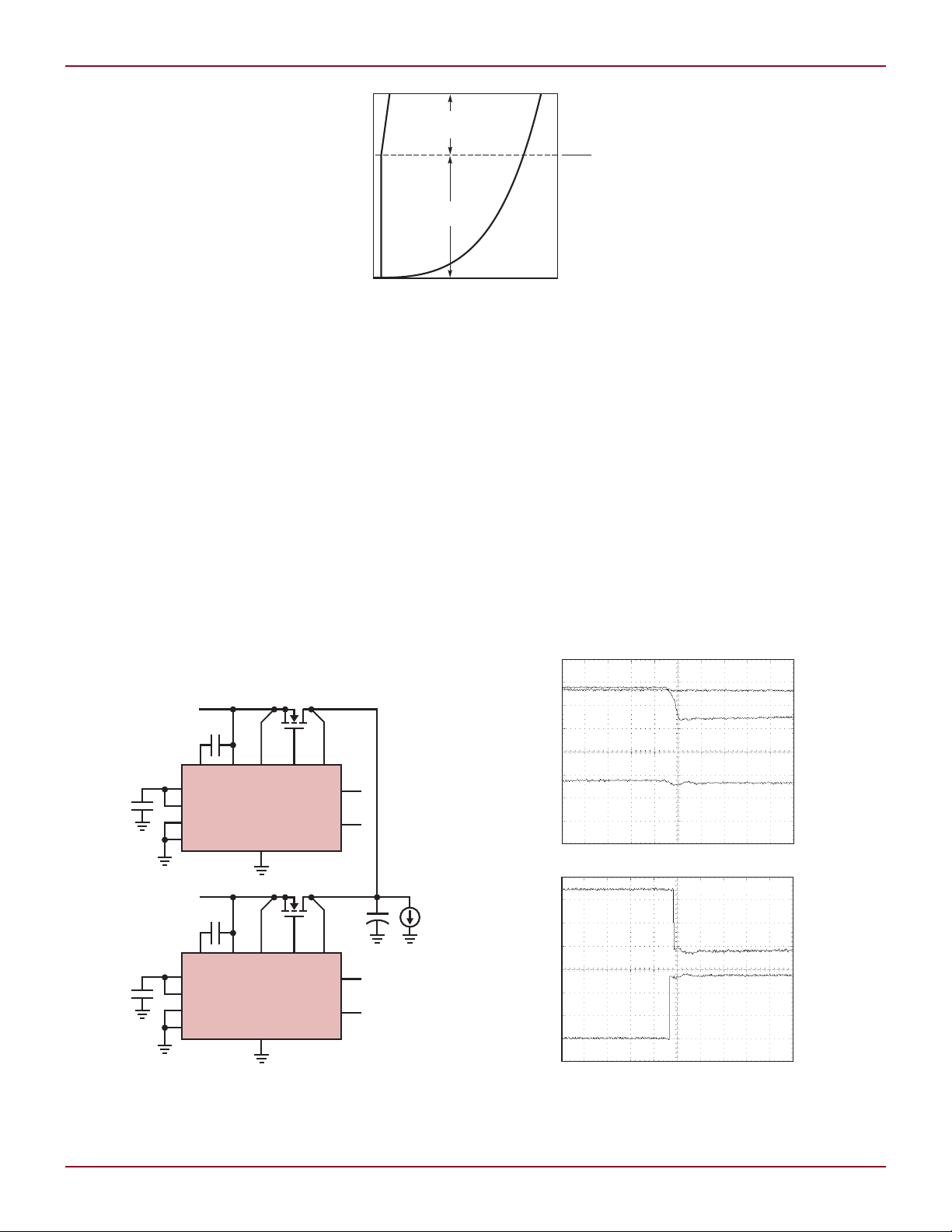
Figure 4. The forward I-V characteristic of the
LTC4352 ideal diode vs a Schottky diode.
The LTC4352 implements a linear
control method to avoid the problems
of the comparator-based technique.
It servos the gate of the MOSFET to
maintain the forward voltage drop
across the MOSFET at 25mV (AMP
of Figure 3). At light load currents,
the gate of the MOSFET is slightly
above its threshold voltage to create a resistance of 25mV/I
LOAD
. As
the load current increases, the gate
voltage rises to reduce the MOSFET
resistance. Ultimately, at large load
currents, the MOSFET gate is driven
fully on, and the forward voltage drop
rises linearly with load current as I
• R
. Figure 4 shows the resulting
DS(ON)
LOAD
ideal diode I-V characteristic.
In a reverse voltage condition, the
gate is servoed low to completely turn
off the MOSFET, thus avoiding DC
reverse current. The linear method
also provides a smooth switchover
of currents for slowly crossing input
supplies in diode-OR applications. In
fact, depending on MOSFET and trace
impedances, the input supplies share
the load current when their voltages
are nearly equal.
Fast Switch Control
Most ideal diode circuits suffer slower
transient response compared to conventional diodes. The LTC4352, on
the other hand, responds quickly to
changes in the input to output voltage. A powerful driver turns off the
MOSFET to protect the input supply
and board traces from large reverse
currents. Similarly, the driver turns
on the switch rapidly to limit voltage
droop during supply switchover in
diode-OR applications.
Figure 5 shows a fast switchover
event occurring in a 3.3V ideal diode-
Linear Technology Magazine • September 2008
a. Ideal diode-OR of 3.5V and 3.3V input supply. b. Supply switchover from V
on V
shows minimal disturbance on load voltage.
IN1
Figure 5. Ideal diode-OR fast switchover
IN1
to V
due to short-circuit
IN2
25

L DESIGN FEATURES
UV
LTC4352
FAULT
STATUS
V
CC
31.6k
1%
1k
1%
3.09k
1%
TO LOAD
5V
Q2
Si7336ADPQ1Si7336ADP
0.1 µF
CPOV
IN
SOURCE GATE
FAULT
D1: GREEN LED LN1351C
D2: RED LED LN1261CAL
MOSFET ON
OUT
0.15µF
REV
GND
5V
D2 D1
5V
1k 1k
OV
OR circuit. Initially V
supplies the
IN1
Table 1. Operating state of the LTC4352 ideal diode as indicated by the STATUS and FAULT lights
entire load current since it is higher
than V
. In this state, MOSFET Q1
IN2
is on and Q3 is off. A short circuit
causes V
to collapse below V
IN1
IN2
.
The LTC4352’s fast response shuts
off Q1 and turns on Q3 so that the
load current can now be supplied by
V
. This fast switchover minimizes
IN2
disturbance on the load voltage so that
downstream circuits can continue to
operate smoothly.
To achieve fast switch turn-on,
the LTC4352 uses an internal charge
pump with an external reservoir capacitor. This capacitor is connected
between the CPO and SOURCE pins.
CPO is the output of a charge pump
that can deliver up to 100µA of pullup current. The reservoir capacitor
accumulates and stores charge, which
can be called upon to produce 1.5A of
transient GATE pull-up current during a fast turn-on event. The reservoir
capacitor voltage drops after the fast
turn-on since it charge-shares with
the input gate capacitance (C
ISS
) of
the MOSFET. For an acceptable drop,
the reservoir capacitor value should
be around 10 times the C
of the
ISS
MOSFET.
It is easy to disable fast turn-on.
Omitting the reservoir capacitor slows
down the gate rise time as determined
by the CPO pull-up current charging
C
. Slow gate turn-on may cause the
ISS
load to droop roughly a volt below the
input as current flows through the
MOSFET body diode until the channel
is enhanced. This may be acceptable
LED State
STATUS Green LED FAULT Red LED
at higher input voltage applications,
such as 12V.
Do What No Diode
Has Done Before
The LTC4352 goes above and beyond
the functionality of a diode by incorporating input undervoltage and
overvoltage protection, outputs to
report status and fault information,
open MOSFET detection, and the ability to allow reverse current.
Figure 6 shows the LTC4352 in a 5V
ideal diode circuit with undervoltage
and overvoltage protection. The UV
and OV pins have comparators with a
0.5V trip threshold and 5mV hysteresis
(Figure 3). The resistive dividers from
the input supply to these pins set up an
input voltage window, typically 4.36V
to 5.78V, where the ideal diode function operates. The STATUS pin pulls
low to light up a green LED whenever
the gate is high and power is flowing
through the external MOSFET. For VIN
MOSFET UV/OV
OPEN NO
outside the input voltage window, the
gate is held off and the FAULT pin pulls
low to signal a fault condition. A red
LED, D2, provides visual indication.
Back-to-back MOSFETs are needed to
block conduction through their intrinsic source-to-drain body diodes in the
gate low condition. A single MOSFET,
Q1, could be used in the case where
only a VIN out-of-range indication is
sufficient. But care should be taken
that the load current flowing through
Q1’s body diode, when its gate is low,
does not cause excessive heat dissipation in the MOSFET.
The MOSFET switch could fail open
circuit or its R
years of operation, increasing the voltage drop across the switch. A large drop
also results when excessive current
flows through the MOSFET, possibly
due to an output short circuit. The
LTC4352 detects such failures and
flags it through its FAULT pin. The
open MOSFET detection circuit trips
Ideal Diode
Operating State
OFF NO
ON NO
OFF YES
may degrade over
DS(ON)
whenever it senses more than 250mV
of forward voltage drop across the
MOSFET—even with the gate turned
on. Note that this condition only causes
the FAULT pin to pull low, but no action is taken to turn off the switch.
Table 1 translates STATUS and FAULT
LED status to the operating state of
the LTC4352.
The input at the REV pin configures
the LTC4352’s behavior for reverse
Figure 6. A 5V ideal diode circuit with input undervoltage and overvoltage protection.
Ideal diode function operates for 4.36V < V
26
< 5.78V, else GATE is low.
IN
current. It is tied low for normal diode
operation, which blocks reverse current from flowing through the external
MOSFET. Driving REV above 1V turns
the gate completely on to its limit, even
during reverse current conditions.
Linear Technology Magazine • September 2008

V
CC
UV
OV
REV
LTC4352
STATUS
FAULT
C2
0.1µF
0V TO 18V
5V
Q1
Si7336ADP
TO LOAD
C1
0.1µF
CPO V
IN
SOURCE GATE
GND
OUT
LTC4352
PLUG-IN CARDCONNECTORSBACKPLANE
Q2
Si7336ADPQ1Si7336ADP
TO LOAD
V
IN
UV
CPO
OV
SOURCE GATE OUT
GND
12V
GND
105k
0.1µF
C
G
10k
10Ω
R
G
5.11k
Z1
Z1: DIODES INC. SMAJ12A
TIME (5ms/DIV)
C
LOAD
= 10mF
GATE
LOAD
VOLTAGE
(5V/DIV)
UV
(0.5V/DIV)
SUPPLY
CURRENT
(5A/DIV)
a. Omitting the CPO capacitor and adding an RC network
on the gate allows inrush current control on a Hot Swap board.
Figure 7. Controlling inrush current
DESIGN FEATURES L
b. After short pin makes contact and UV is above 0.5V,
GATE starts ramping up. Once it crosses the MOSFET
threshold voltage, LOAD follows with the same dV/dt.
Here, inrush is limited to 8.3A peak for a 10mF C
LOAD
.
Only undervoltage, overvoltage, and
VCC undervoltage lockout can override
this to turn-off the gate. This feature
is handy either in power path control
applications which allow reverse
current flow to occur, or for testing
purposes.
Inrush Control on a
Hot Swap Board
When the diode power input flows
across a connector on a hot swap
board, the LTC4352 can do doubleduty to control the inrush current.
Again, back-to-back MOSFETs are
required for this application to block
conduction through the MOSFET body
diodes. The inrush current is limited
by slowing the rise rate of the load
voltage. This is done by limiting dV/dt
on the MOSFET gate and operating it
in a source-follower configuration.
Figure 7 illustrates an application where the LTC4352 is used for
inrush control. Since the goal is
to limit dV/dt on the gate, the fast
turn-on characteristic of the ideal
diode is disabled by omitting the CPO
reservoir capacitor. The gate current
is now limited to the CPO pull-up
current of 100µA. To further reduce
dV/dt, an RC network is added on
the gate. The resistor decouples the
capacitor during fast turn-off due to
reverse current or overvoltage faults.
Linear Technology Magazine • September 2008
Resistor RG prevents high frequency
oscillations in Q2.
When the board is hot-plugged, the
long power pins make contact first.
The LTC4352 powers up, but holds
the gate off since UV is low. After a few
milliseconds of board insertion delay,
the short UV pin makes contact. If
VIN is above 10.8V, the MOSFET gate
starts ramping up. The MOSFET turns
on as the gate reaches the threshold
voltage, and current starts charging
the output. Q2 operates in the source
follower mode and suffers the most
power dissipation. Its VDS starts off
at VIN and decreases to 25mV/2.
Care should be taken that the power
dissipated during inrush falls within
the safe operating area (SOA) of the
MOSFET.
Figure 8. A 0V to 18V ideal diode circuit. By powering the VCC pin with an external
supply in the 4.7V to 6V range (here 5V), VIN can operate down to 0V and up to 18V.
Down to Earth Operation
The VIN operating range extends all
the way down to 0V. However, when
operating with inputs below 2.9V,
an external supply is needed on the
VCC pin. This supply should be in the
range 2.9V to 6V. For a 2.9V to 4.7V
subset of this range, VIN should always
be lower than VCC. A 0.1µF bypass
capacitor is also needed between the
VCC and GND pins. Figure 8 shows an
ideal diode circuit, where a 5V supply
powers up the VCC pin. In this case,
VIN can operate all the way down to
0V and up to 18V.
For input supplies from 2.9V to 18V,
the external supply at the VCC pin is
not needed. Instead, an internal low
dropout regulator (LDO in Figure 3)
continued on page 31
27

DESIGN IDEAS L
bias supply. Another boost converter
and an inverter generate VON and
V
, which also use the 5V supply
OFF
as input.
When power is first applied to the
input, the RUN-SS1 capacitor starts
charging. When its voltage reaches
0.8V, Switcher 1 is enabled. The capacitor at the RUN-SS1 pin controls
the ramp rate for the Switcher 1 output, V
and inrush current in L1.
LOGIC
Switchers 2, 3 and 4 are controlled
by the BIAS pin, which is usually
connected to V
. When the BIAS
LOGIC
pin is higher than 2.8V, the capacitors
at the RUNSS-2 and RUN-SS3/4 pin
begin charging to enable Switchers 2,
3 and 4. When AV
reaches 90% of
DD
its programmed voltage, the PGOOD
pin is pulled low. When AV
DD
, V
OFF
and
E3 all reach 90% or their programmed
voltages, the C
timer is enabled and a
T
20µA current source begins to charge
CT. When the C
pin reaches 1.1V, the
T
output PNP turns on, connecting E3
to VON. Figure 2 shows the start up
sequence of the circuit in Figure 1.
If one of the regulated voltages,
V
LOGIC
, AV
DD
, V
or E3 dips more
OFF
than 10%, the internal PNP turns off
to shut down VON. This action protects
the panels, as V
must be present to
ON
turn on the TFT display. The PGOOD
pin can drive an optional PMOS device
at the output of the boost regulator to
disconnect the load at AV
from the
DD
input during shutdown. The converter
uses all ceramic capacitors. X5R and
X7R types are recommended, as these
materials maintain capacitance over
a wide temperature range.
All four switchers employ a constant frequency, current mode control
scheme. Switching regulator 1 uses a
feedback scheme that senses inductor current, while the other switching
regulators monitor switch current.
The inductor current sensing method
avoids minimum on-time issues and
maintains the switch current limit at
any input-to-output voltage ratio. The
other three regulators have frequency
foldback scheme, which reduces the
switching frequency when its FB pin
is below 0.75V. This feature reduces
the average inductor current during
start up and overload conditions,
minimizing the power dissipation
in the power switches and external
components.
Layout Considerations
Proper PC board layout is important
to achieve the best operating performance. Paths that carry high switching
current should be short and wide to
minimize parasitic inductance. In a
buck regulator, this loop includes
the input capacitor, internal power
switch and Schottky diode. In a boost
regulator, this loop includes the output capacitor, internal power switch
and Schottky diode. Keep all the loop
compensation components and feedback resistors away from the high
switching current paths. The LT3513
pin out was designed to facilitate PCB
layout. Keep the traces from the center
of the feedback resistors to the corresponding FB pins as short as possible.
LT3513 has an exposed ground pad
on the backside of the IC to reduce
thermal resistance. A ground plane
with multiple vias into ground layers
should be placed underneath the part
to conduct heat away from the IC.
Conclusion
The LT3513 is a comprehensive, but
compact, power supply solution for
TFT-LCD panels. Its wide input range
and low power dissipation allow it
to be used in a wide variety of applications. All four of the integrated
switching regulators have a 2MHz
switching frequency and allow the
exclusive use of the ceramic capacitors to minimize circuit size, cost and
output ripple.
L
LTM4604, LTM4608, continued from page 29
than 5% at full load. Excellent cur-
leled LTM4608 boards supplying 16A
output current.
rent sharing results in well balanced
thermal stresses on the paralleled
LTM4608s, which in turn makes
for a more reliable system. Figure 7
demonstrates the small temperature
difference between these two paral-
LTC4352, continued from page 27
generates a 4.1V supply at the VCC
pin. For VIN below 4.1V, VCC follows
approximately 50mV below VIN. The
0.1µF VCC capacitor is still needed for
bypassing and LDO stability.
Conclusion
The LTM4604 and LTM4608 15mm
× 9mm µModule regulators are complete power supply solutions for low
input voltage and high output cur-
trend has been to lower the voltage of
distributed power, which increases the
current to maintain power levels. Given
these constraints, board designers
must scrutinize each diode in a high
current power path for its power and
area consumption.
Conclusion
An ever-present theme in electronic
system design has been to pack more
computation in smaller form factors
and tighter power budgets. Another
Linear Technology Magazine • September 2008
provides the same functionality as a
diode but at higher efficiencies and
cooler temperatures, especially as
currents increase. It also incorporates
The LTC4352 MOSFET controller
rent applications. They significantly
simplify circuit and layout designs
by effortlessly fitting into the tightest
spaces, including the bottom of the
PCB. Despite their compact form,
these µModules are rich in features,
and they can be easily paralleled when
more output current is needed.
L
useful features such as fast switch
control, 0V operation, undervoltage
and overvoltage protection, open
MOSFET detection, ability to allow
reverse current, Hot Swap capability, and fault and status outputs. All
of this functionality comes wrapped
in space-saving 12-pin DFN (3mm ×
3mm) and MSOP packages, making
it possible to produce an ideal diode
solution in a smaller footprint than
conventional diodes.
L
3131
 Loading...