

FEATURES
LTC4350
Hot Swappable
Load Share Controller
U
DESCRIPTIO
■
Build N + 1 Redundant Supply
■
Hot SwapTM Power Supplies
■
Isolates Supply Failures from Output
■
Eliminates ORing Diodes
■
Identifies and Localizes Output Low, Output High
and Open-Circuit Faults
■
Output Voltages from 1.5V to 12V
■
16-Lead Narrow SSOP Package
U
APPLICATIO S
■
Servers and Network Equipment
■
Telecom and Base Station Equipment
■
Distributed Power Systems
U
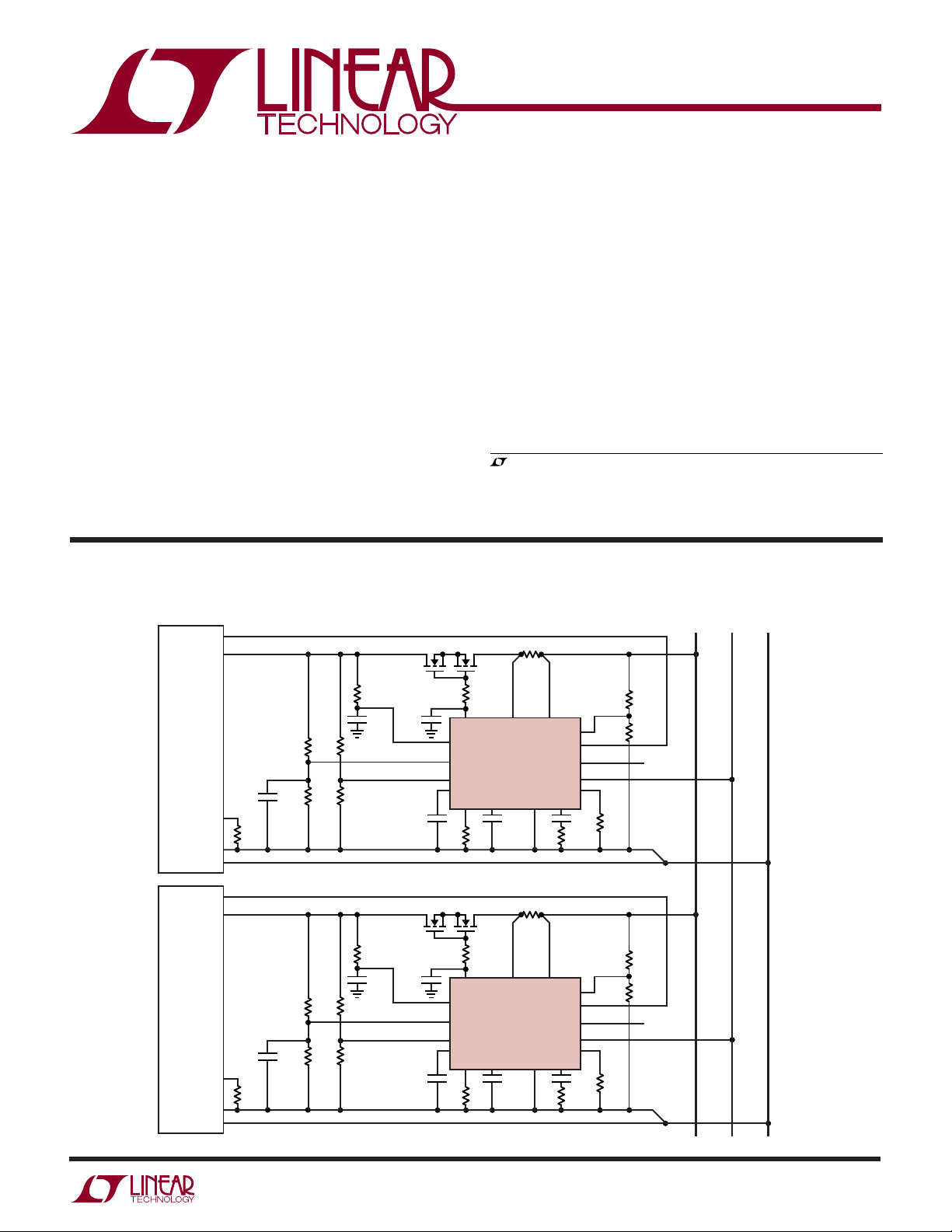
TYPICAL APPLICATIO
5V Load Share (5A per Module)
+
SENSE
+
OUT
SUD50N03-07
The LTC®4350 is a load share controller that allows
systems to equally load multiple power supplies connected in parallel. The output voltage of each supply is
adjusted using the SENSE+ input until all currents match
the share bus. The LTC4350 also isolates supply failures
by turning off the series pass transistors and identifying
the failed supply. The failed supply can then be removed
and replaced with a new unit without turning off the
system power. The LTC4350 is available in a 16-pin
narrow SSOP package.
, LTC and LT are registered trademarks of Linear Technology Corporation.
Hot Swap is a trademark of Linear Technology Corporation.
0.010Ω
V
OUT
+
SHARE BUS
–
V
OUT
VICOR*
VI-J30-CY
SENSE
SENSE
VICOR*
VI-J30-CY
SENSE
51Ω 100Ω
0.1µF
0.1µF
43.2k
274k
12.1k
121k
0.1µF
TRIM
470k
–
–
OUT
+
+
OUT
43.2k
274k
0.1µF
TRIM
470k
–
–
OUT
*LOAD SHARING CIRCUIT WORKS WITH MOST POWER SUPPLIES THAT HAVE A SENSE
12.1k121k
0.1µF
SUD50N03-07
51Ω 100Ω
0.1µF
0.1µF
0.1µF
–
34k
34k
R+R
LTC4350
1000pF
0.010Ω
R+R
LTC4350
1000pF
STATUS STATUS
–
STATUS STATUS
+
OR FB PIN
GATE
V
CC
UV
OV
TIMER
GAIN COMP1 GND COMP2
GATE
V
CC
UV
OV
TIMER
GAIN COMP1 GND COMP2
37.4k
FB
I
OUT
SB
R
SET
4.7µF
150Ω
FB
I
OUT
SB
R
SET
4.7µF
150Ω
12.1k
100Ω
37.4k
12.1k
100Ω
4350 TA01
4350fa
1
Note 1: A
LTC4350
WW
W
U
ABSOLUTE MAXIMUM RATINGS
(Note 1)
Supply Voltage (VCC) ............................................... 17V
Input Voltage
TIMER .................................................. –0.3V to 1.2V
R+, R– (Note 2) ......................................–0.3V to 17V
FB ........................................................ – 0.3V to 5.3V
OV, UV ....................................................... –0.3V to 17V
Output Voltage
COMP1 ................................................... – 0.3V to 6V
COMP2 ................................................... – 0.3V to 3V
GAIN, SB ............................................. –0.3V to 5.6V
GATE (Note 3) ...........................................– 0.3V to 20V
I
, STATUS ........................................... – 0.3V to 17V
OUT
R
.......................................................................
SET
Operating Temperature Range
LTC4350C ............................................... 0°C to 70°C
LTC4350I........................................... – 40°C to 85°C
Storage Temperature Range ................. –65°C to 150°C
Lead Temperature (Soldering, 10 sec).................. 300°C
–0.3V to 1V
U
W
U
PACKAGE/ORDER INFORMATION
TOP VIEW
1
UV
2
OV
3
TIMER
4
GAIN
5
COMP2
6
COMP1
7
SB
8
GND
GN PACKAGE
16-LEAD PLASTIC SSOP
T
= 150°C, θJA = 135°C/W
JMAX
Consult LTC marketing for parts specified with wider operating temperature ranges.
16
15
14
13
12
11
10
9
V
CC
STATUS
GATE
+
R
–
R
I
OUT
R
SET
FB
ORDER PART
NUMBER
LTC4350CGN
LTC4350IGN
GN PART MARKING
4350
4350I
ELECTRICAL CHARACTERISTICS
The ● denotes the specifications which apply over the full operating
temperature range, otherwise specifications are at TA = 25°C. VCC = 5V unless otherwise noted.
SYMBOL PARAMETER CONDITIONS MIN TYP MAX UNITS
DC Characteristics
I
CC
V
LKOH
V
LKOL
V
FB
V
FBLIR
V
FBLOR
V
UVTH
V
OVTH
V
TM
I
TM
V
G
V
GO
V
SB(MIN)
V
SB(MAX)
I
SB(MAX)
R
SB
V
E/A2OFF
VCC Supply Current UV = V
VCC Undervoltage Lockout High ● 2.36 2.45 2.52 V
VCC Undervoltage Lockout Low ● 2.24 2.34 2.44 V
FB Pin Voltage 0°C to 85°C (LTC4350I) or 0°C to 70°C (LTC4350C) 1.208 1.220 1.236 V
FB Line Regulation VCC = 3.3V to 12V, COMP1 = 1.240V 0.02 0.05 %/V
FB Load Regulation COMP1 = 2V ● –0.0008 –0.1 %
UV Pin Threshold High Going Threshold ● 1.215 1.244 1.258 V
OV Pin Threshold High Going Threshold ● 1.203 1.220 1.250 V
TIMER Pin Threshold ● 1.18 1.22 1.26 V
TIMER Pin Current TIMER On, V
GAIN Pin Voltage R
GAIN Pin Offset R
SB Pin Minimum Voltage 28 mV
SB Pin Maximum Voltage VCC = 3.3V ● 2.4 2.7 2.9 V
SB Pin Maximum Current V
SB Pin Resistor Value ● 14 20 33 kΩ
E/A2 Offset VSB – V
CC
–40°C to 85°C (LTC4350I) 1.196 1.220 1.244 V
COMP1 = 0.64V
Low Going Threshold
Low Going Threshold
= 0V ● –1.75 – 2 –2.3 µA
TIMER
TIMER On, V
= 25k, (V
GAIN
= 25k, (V
GAIN
VCC = 12V ● 5.6 7.8 10.5 V
= 0V ● –8 –33 –41 mA
SB
GAIN
= 0V, VOV > V
TIMER
+
– V
R
+
– V
R
–
R
–
R
OVTH
) = 100mV ● 2.3 2.5 2.7 V
) = 0mV ● 0 0.02 0.20 V
● 1.0 1.6 2.0 mA
● 0.003 0.1 %
● 1.205 1.220 1.237 V
● 1.180 1.205 1.229 V
● – 5.30 – 6 – 6.7 µA
● 82550 mV
2
4350fa
LTC4350
ELECTRICAL CHARACTERISTICS
The ● denotes the specifications which apply over the full operating
temperature range, otherwise specifications are at TA = 25°C. VCC = 5V unless otherwise noted.
SYMBOL PARAMETER CONDITIONS MIN TYP MAX UNITS
DC Characteristics
V
RSET(MAX)RSET
V
RSET(MIN)RSET
I
RSET(MAX)RSET
V
RCTH
∆V
GATE
I
GATE
V
SOL
Note 1: Absolute Maximum Ratings are those values beyond which the life
of a device may be impaired.
Note 2: R
Pin Maximum Voltage VCC = 3.3V, R
V
Pin Minimum Voltage VCC = 5V, R
V
Pin Maximum Current R
Reverse Current Threshold V
External N-Channel Gate Drive V
GATE Pin Current Gate On, V
STATUS Pin Output Low I
+
and R– could be at 17V while VCC = 0V.
OUT
= 100Ω ● 0.94 1 1.03 V
– V
SET
= 100Ω ● 0.94 1 1.03 V
SET
= 1000Ω ● 0.001 0.5 V
SET
= 100Ω ● 0.001 0.5 V
SET
= 1.1V ● 18 20 21 mA
IOUT
+
R
CC
= 0V ● –8 –10 –12 µA
GATE
● 10 30 40 mV
● 10.8 12 12.7 V
= 12V, R
CC
= 5V, R
CC
= 50Ω, V
SET
+
– V
R
GATE
= 3mA ● 0.1 0.3 1.2 V
Note 3: An internal clamp limits the GATE pin to a minimum of 10.8V
above V
. Driving this pin to voltages beyond the clamp may damage the
CC
part.
UW
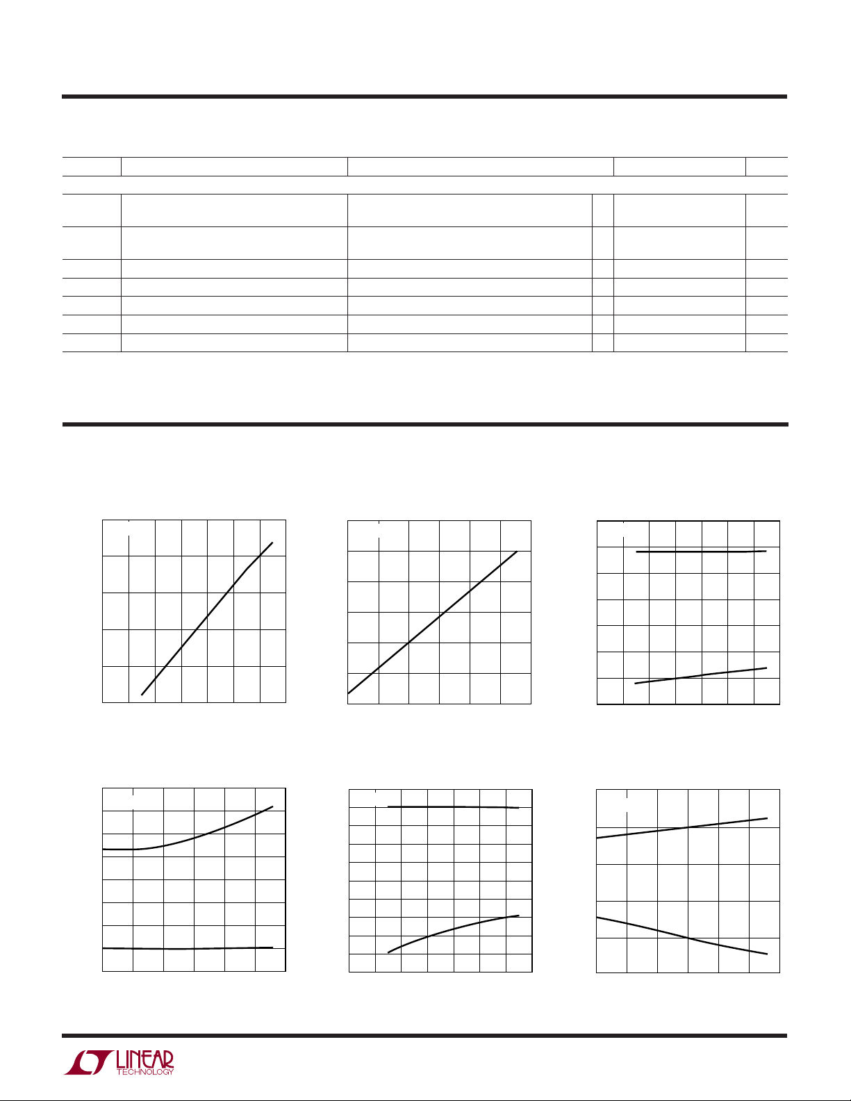
TYPICAL PERFOR A CE CHARACTERISTICS
3.5
3.0
2.5
(mA)
CC
I
2.0
1.5
ICC vs V
TA = 25°C
CC
ICC vs Temperature UV Threshold vs V
1.66
1.64
1.62
1.60
(mA)
CC
I
1.58
1.56
VCC = 5V
1.250
TA = 25°C
1.245
1.240
1.235
1.230
UV THRESHOLD (V)
1.225
1.220
CC
1.0
02
4
VCC (V)
10
8
6
12
14
4350 G01
1.54
–50
–25 0
UV Threshold vs Temperature OV Threshold vs V
1.255
VCC = 5V
1.250
1.245
1.240
1.235
1.230
UV THRESHOLD (V)
1.225
1.220
1.215
–50
–25
02550
TEMPERATURE (°C)
75 100
4350 G04
1.222
TA = 25°C
1.220
1.218
1.216
1.214
1.212
1.210
OV THRESHOLD (V)
1.208
1.206
1.204
1.202
02
25 75
TEMPERATURE (°C)
CC
8
6
4
VCC (V)
50 100
4350 G02
12
14
4350 G05
10
1.215
02
6
4
VCC (V)
OV Threshold vs Temperature
1.225
VCC = 5V
1.220
1.215
1.210
OV THRESHOLD (V)
1.205
1.200
–50
02550
–25
TEMPERATURE (°C)
8
10
14
12
4350 G03
75 100
4350 G06
4350fa
3
LTC4350
VCC (V)
02
2.2
GAIN (V)
2.4
2.7
4
8
10
4350 G09
2.3
2.6
2.5
6
12
14
R
GAIN
= 25k
(V
R
+
– V
R
–
) = 100mV
T
A
= 25°C
UW
TYPICAL PERFOR A CE CHARACTERISTICS
FB vs V
CC
1.230
TA = 25°C
1.225
1.220
FB (V)
1.215
1.210
02
4
VCC (V)
10
8
6
12
14
4350 G07
Gain Pin Voltage vs Temperature ∆V
2.7
R
= 25k
GAIN
+
–
– V
) = 100mV
(V
R
R
= 5V
V
CC
2.6
2.5
GAIN (V)
2.4
2.3
FB vs Temperature Gain PIn Voltage vs V
1.230
VCC = 5V
1.225
1.220
FB (V)
1.215
1.210
(V)
GATE
∆V
13
12
11
10
9
8
7
–50
GATE
TA = 25°C
02550
–25
TEMPERATURE (°C)
vs V
CC
75 100
4350 G08
(V)
GATE
∆V
13.0
12.5
12.0
11.5
∆V
vs Temperature
GATE
VCC = 5V
CC
2.2
–50
U
02550
–25
TEMPERATURE (°C)
75 100
4350 G10
UU
6
0
24
PI FU CTIO S
UV (Pin 1): Undervoltage Pin. The threshold is set at
1.244V with a 24mV hysteresis. When the UV pin is pulled
high, the charge pump ramps the GATE pin. When the UV
pin is pulled low, the GATE pin will be pulled low.
OV (Pin 2): Overvoltage Pin. The threshold is set at 1.220V
with a 15mV hysteresis. When the OV pin is pulled high,
the GATE pin is pulled low. After a timer cycle, the STATUS
pin is pulled low until the OV pin is pulled low.
TIMER (Pin 3): Analog System Timing Generator Pin. This
pin is used to set the delay before the load sharing turns
on after the UV pin goes high. The other use for the TIMER
pin is to delay the indication of a fault on the STATUS pin.
81214
610
VCC (V)
4350 G11
11.0
–50
02550
–25
TEMPERATURE (°C)
75 100
4350 G12
When the timer is off, an internal N-channel shorts the
TIMER pin to ground. When the timer is turned on, a 2µA
or 6µA timer current (I
) from VCC is connected to the
TIMER
TIMER pin and the voltage starts to ramp up with a slope
given by: dV/dt = I
TIMER/CT
. When the voltage reaches the
trip point (1.220V), the timer will be reset by pulling the
TIMER pin back to ground. The timer period is given by:
(1.220V • CT)/I
TIMER
.
GAIN (Pin 4): Analog Output Pin. The voltage across the
R+ and R– pins is divided by a 1k resistor and sourced as
a current from the GAIN pin. An external resistor on the
GAIN pin determines the voltage gain from the current
sense resistor to the GAIN pin.
4350fa
4

LTC4350
U
UU
PI FU CTIO S
COMP2 (Pin 5): Analog Output Pin. This pin is the output
of the share bus error amplifier E/A2. (A compensation
capacitor between this pin and ground sets the crossover
frequency for the power supply adjustment loop.) In most
cases, this pin operates between 0.5V to 1.5V and represents a diode voltage up from the voltage at the R
It is clamped at 3V. During start-up, this pin is clamped to
ground. After a timer cycle (and if the GATE pin is high), the
COMP2 pin is released.
COMP1 (Pin 6): Analog Output Pin. This pin is the output
of the voltage regulating error amplifier E/A1. A compensation capacitor between this pin and ground sets the
crossover frequency of the share bus loop. This pin
operates a diode voltage up from the voltage at the SB pin
and is clamped at 8.4V.
SB (Pin 7): Analog Output Pin. This pin drives the share
bus used to communicate the value of shared load current
between several power supplies. There is an amplifier that
drives this pin a diode below the COMP1 pin using an
internal NPN as a pull-up and a 20k resistor as a pull-down.
GND (Pin 8): Chip Ground.
FB (Pin 9): Analog Error Amplifier Input (E/A1). This pin is
used to monitor the output supply voltage with an external
resistive divider. The FB pin voltage is compared to 1.220V
reference. The difference between the FB pin voltage and
the reference is amplified and output on the COMP1 pin.
R
(Pin 10): Analog Output Pin. The I
SET
OUT
converts the voltage at the COMP2 pin (down a diode
voltage) to the R
external resistor (R
ground is (COMP2 – V
pin. Therefore, the current through the
SET
) placed between the R
SET
DIODE
)/R
. This current is used to
SET
SET
adjust the output voltage.
I
(Pin 11): Analog Output Pin. The current flowing into
OUT
the I
pin that was set by the external resistor R
pin is equal to the current flowing out of the R
OUT
. This current
SET
is used to adjust the output supply voltage by modifying
the voltage sensed by the power supply’s internal voltage
feedback circuitry.
pin.
SET
amplifier
pin and
SET
R– (Pin 12): Analog Input Pin. With a sense resistor placed
in the supply path between the R+ and R– pins, the power
supply current is measured as a voltage drop between R
and R–. This voltage is measured by the I
SENSE
block and
+
multiplied at the GAIN pin.
+
(Pin 13): Analog Input Pin. With a sense resistor placed
R
in the supply path between the R
supply current is measured as a voltage drop between R
and R–. This voltage is measured by the I
+
and R– pins, the power
block and
SENSE
+
multiplied at the GAIN pin.
GATE (Pin14): The high side gate drive for the external
N-Channel power FET. An internal charge pump provides
the gate drive necessary to drive the FETs. The slope of the
voltage rise or fall at the GATE is set by an external
capacitor connected between GATE and GND, and the
10µA charge pump output current. When the undervoltage
lockout circuit monitoring V
trips, the OV pin is pulled
CC
high or the UV pin is pulled low, the GATE pin is immediately pulled to GND.
STATUS (Pin 15): Open-Drain Digital Output. The STATUS pin has an open-drain output to GND. This pin is
pulled low to indicate a fault has occurred in the system.
There are three types of faults. The first is a undervoltage
lockout on VCC or the UV pin is low while the output
voltage is active. The second is when the COMP2 pin is
above 1.5V or below 0.5V and the voltage on the GAIN pin
is greater than 100mV. The final failure is when the OV pin
is high. The three faults will activate the pull-down on the
STATUS pin after a timing cycle.
VCC (Pin 16): The Positive Supply Input, Ranging from
3.3V to 12V for Normal Operation. ICC is typically 1.6mA.
An undervoltage lockout circuit disables the chip until the
voltage at VCC is greater than 2.47V. A 0.1µF bypass
capacitor is required on the VCC pin. If the VCC pin is tied
to the same power supply output that is being adjusted,
then a 51Ω decoupling resistor is needed to hold up the
supply during a short to ground on the supply output. V
CC
must be greater than or equal to the supply that is
connected to the R+ and R– pins.
4350fa
5

LTC4350
BLOCK DIAGRA
W
6
9
1
COMP1
FB
–
R
UV
V
CC
REF
+
–
+
–
REVERSE CURRENT
+
R
30mV
+
–
+
–
–
E/A1
E/A2
1416
GATE
CHARGE
PUMP
OVER/UNDER
CURRENT
13
12
+
–
R
R
+
I
OUT
+
I
SENSE
20k
–
gm = 1m
Ω
GAIN
COMP2
I
OUT
4
SB
7
5
11
–
R
SET
10
6
REF
OV
2
REF
+
+
2µA/6µA
LOGIC
–
GND
8
TIMER
STATUS
3
15
4350 BD
4350fa

WUUU
APPLICATIO S I FOR ATIO
LTC4350
INTRODUCTION
Many system designers find it economically feasible to
parallel power supplies to achieve redundancy. The second trend is providing some load sharing between the
many supplies. In some cases, a failure in any one supply
will trigger a sequence that disconnects the faulty supply
and sends a flag to the system. Then, a service technician
will swap in a good supply. For systems that are continuously powered, there is Hot Swap circuitry to prevent
glitches on the power buses when power cards are
swapped. A block diagram of this system is shown in
Figure 1.
By combining the features of a load share and a Hot Swap
controller into one IC, the LTC4350 simplifies the design
of redundant power supplies. A complete redundant power
supply is a combination of a power module and the
LTC4350 as shown in Figure 2. Note that the power
CONNECTOR
LOAD
HOT
SWAP
CONNECTOR
HOT
SWAP
OUTPUT
SHARE
BUS
Figure 1. Redundant Power Card System
INPUT BUS
OUTPUT BUS
SHARE BUS
INPUT
BUS
BUS
POWER
MODULE
+
OUT
+
SENSE
–
SENSE
–
OUT
Figure 2. Redundant Power Supply
LOAD
SHARE
LOAD
SHARE
LTC4350
4350 F02
POWER
SUPPLY
POWER
SUPPLY
4350 F01
module must have accessible feedback network or a
remote sensing pin (SENSE+) to interface to the LTC4350.
The LTC4350 provides a means for paralleling power
supplies. It also provides for load sharing, fault isolation
and power supply hot insertion and removal. The power
supply current is accurately measured and then compared
to a share bus signal. The power supply’s output voltage
is adjusted until the load current matches the share bus,
which results in load sharing. There are two optional
power FETs in series with the load that provide a quick
disconnect between a load and a failed power supply.
These same power FETs allow a power supply to be
connected into a powered backplane in a controlled manner or removed without disruption.
CURRENT SHARING
The current sharing components will now be discussed.
Figure 3 shows a simplified block diagram of these components. The I
block measures the power supply
SENSE
current by amplifying the voltage drop across the sense
resistor. An external resistor on the GAIN pin determines
the gain of the I
block. The voltage drop across the
SENSE
sense resistor is divided by a precision 1k resistor to
produce a current at the GAIN pin. For example, a 10mV
sense voltage translates to a 10µA current. If a 10k resistor
is on the GAIN pin, then the voltage gain is 10k/1k or 10.
The voltage at the GAIN pin is compared to the current
share bus using the E/A2 block. The output of E/A2 is used
to adjust the output voltage of the power supply using the
I
block. The objective of the E/A2 block is forcing the
OUT
GAIN pin voltage to equal the SB pin voltage. When the
GAIN pin voltages of all the LTC4350s in the system equal
the SB pin voltage, the load current is shared.
VOLTAGE MONITOR
Unique to the LTC4350 is tight output voltage regulation.
This is handled by the LTC4350’s error amplifier and
reference and not the power supply’s error amplifier and
reference. The E/A1 amplifier monitors the output voltage
via the feedback divider connected to the FB pin. The FB pin
is compared to the internal reference of the LTC4350. If the
FB pin is at or below the reference, then the output of E/A1
4350fa
7

LTC4350
WUUU
APPLICATIO S I FOR ATIO
PASS-FET USED TO
DISCONNECT A BAD POWER
SUPPLY AND TO HOT-SWAP A
+
OUT
THE POWER SUPPLY CURRENT
POWER SUPPLY
C
G
GATE
DRIVE
THIS VOLTAGE REPRESENTS
MEASURED USING A SENSE
3
+
RESISTOR
R
I
SENSE
SENSE
21
–
gm = 1m
R
GAIN
R
OUT
+
SENSE
4
FB PIN
Ω
–
E/A1
+
REF
+
E/A2
–
THIS VOLTAGE REPRESENTS
THE
REFERENCE CURRENT
(i.e., SHARE BUS)
VALUE
NEEDED TO FORCE THE OUTPUT
VOLTAGE TO EQUAL THE REF
COMP1 PIN
20k
COMP2 PIN
+
I
OUT
SHARE BUS
I
OUT
PIN
–
THIS AMPLIFIER FORCES THE POWER
SUPPLY CURRENT TO EQUAL THE
REFERENCE CURRENT VALUE
(i.e., SHARE BUS)
+–
I
ADJ
LOAD
THIS RESISTOR CONVERTS I
TO A VOLTAGE TO MODIFY THE
REMOTE SENSE INPUT OF THE
POWER SUPPLY (SENSE
CREATES AN ARTIFICIAL
+
VOLTAGE THAT
SENSE
ADJUSTS THE POWER
SUPPLY’S OUTPUT VOLTAGE
UP OR DOWN
THIS AMPLIFIER CONVERTS
THE E/A2 VOLTAGE OUTPUT TO
A CURRENT OUTPUT (I
R
PIN
SET
R
SET
4350 F03
ADJ
ADJ
+
). IT
)
Figure 3. Simplified Block Diagram
drives the SB pin (or share bus). If the FB pin is above the
reference, the COMP1 pin is grounded and the SB pin is
disconnected from the COMP1 pin using the series diode.
The LTC4350 with the highest reference will drive the SB
pin and the 20k loads connected to the SB pin. All of the
other LTC4350’s COMP1 pins are pulled low because their
FB pins are at a higher voltage than their references. The
series diode between the COMP1 pin and the SB pin is
actually a low impedance buffer amplifier with a diode in
the output stage. Therefore, the master LTC4350’s E/A1
drives the share bus to the proper value that keeps the
output voltage tightly regulated. The buffer amplifier is
capable of driving at least fifty 20k loads (each 20k load
represents an LTC4350).
OUTPUT VOLTAGE ADJUSTMENT
The LTC4350 is designed to work with supplies featuring
remote sense. The output voltage of each power supply
needs to be adjusted below the final output voltage at the
common load. For example, a 5V system would require the
power supply output be set to 4.90V or some value below
5V. This is normally done using the trim pin of the module.
The power supply output is then increased by artificially
reducing the positive sense voltage by a small amount.
The LTC4350 would then adjust the output voltage to 5V,
an increase of 2%. The maximum range of adjustment can
be set from 2% to 5% to compensate for voltage drops in
the wiring, but no more than 300mV.
In most power supplies, the voltage sense is tied directly
to the output voltage. If a small valued resistor, R
OUT
, is
placed in series with the power supply sense line, a voltage
drop across R
appears as a lower sensed voltage. This
OUT
requires the power supply to increase its output voltage to
compensate. Thus, the LTC4350 exercises complete control of the final output voltage.
The I
a current that flows through R
voltage at COMP2 increases, the current in R
block converts the E/A2 output (COMP2 pin) to
OUT
(see Figure 3). As the
OUT
OUT
4350fa
8

WUUU
APPLICATIO S I FOR ATIO
LTC4350
increases. The output voltage will then increase by an
amount equal to the voltage drop across R
external resistor, R
tionship in the I
as I
ADJ
= (V
OUT
COMP2
, sets the voltage to current rela-
SET
block. The current in R
– 0.58V)/R
SET
.
OUT
The maximum voltage that can be applied across R
. The
OUT
is defined
is
SET
1V. The range of the output voltage adjustment is set to be
V
MAXADJ
voltage if the share bus is accidentally shorted to V
= R
OUT/RSET
. This sets the worst-case output
. As
CC
mentioned previously, this range is set to be 2% to 10%
in value.
The compensation elements, C
CP1
and C
, are used to
CP2
set the crossover frequencies of the two error amplifiers
E/A1 and E/A2. In the Design Example section, the
calculations for choosing all of the components will be
discussed.
Output Adjust Soft-Start
In the LTC4350, there is soft-start circuitry that holds the
COMP2 pin at ground until both the GATE pin is 4V above
the VCC pin and a timer cycle is completed following the
UV pin becoming active.
In cases where the power FETs are turned on but the
power supply is still ramping up, the load voltage may
overshoot. For these cases, the COMP2 pin is clamped to
ground during one timing cycle. If the UV pin is greater
than 1.244V, the chip begins the timer cycle. The timer
cycle uses a 2µA current source into an external capacitor
on the TIMER pin. As soon as the voltage at the TIMER pin
exceeds 1.220V, the timer cycle is over. The time-out is
defined as t = C
• 1.220V/2µA. At the end of the timer
T
cycle, the power supply ramping should be complete.
Faults
There are several types of power supply output faults.
Shorts from the output to ground or to a positive voltage
greater than the normal output voltage are considered
“hard faults.” These faults require the bad power supply to
be immediately disconnected from the load in order to
prevent disruption of the system. “Soft faults” include
power supply failed open-circuit or load current sharing
failure where the output voltage is normal but load sharing
between several supplies is not equal. The LTC4350 can
isolate soft and hard faults and signal a system controller
using the STATUS pin.
Upon power-up, most of the circuitry is active including
the circuits that monitor and adjust the output voltage.
The external power FETs are initially open circuit when
power is applied. It takes about 10ms to 100ms for the
FETs to transition from the off to the fully on state (as
discussed in the following Hot Swapping section). During this time the FB pin is near ground which forces the
SB to the positive rail. The COMP2 pin is then forced to
the positive rail, which forces the R
pin to 1V. The
SET
voltage at the output of the power supply is now adjusted
to its maximum adjusted value, which can be 10% above
nominal. Once the power FETs are turned on, the load will
see this adjusted output voltage. This appears to be a
voltage overshoot at the load that exists until the loop can
correct itself. The dominant pole in the loop exists on the
COMP2 pin. Therefore, the overshoot duration is determined by the discharge time of the COMP2 pin.
In order to eliminate this overshoot, the COMP2 pin is
clamped at ground until the GATE pin is 4V above the V
CC
pin (power FETs are turned on). Now, the COMP2 pin will
begin to charge up until the FB pin regulates at 1.220V.
HARD FAULTS
The LTC4350 can identify faults in the power supply and
isolate them from the load if optional external power FETs
are included between the power supply and the load. In the
case of a power supply output short to ground, the reverse
current block will sense that the voltage across the current
sense resistor has changed directions and has exceeded
30mV for more than 5µs. The gate of the external power
FETs is immediately pulled low disconnecting the short
from the load. The gate is allowed to ramp-up and turn-on
the power FETs as soon as the reverse voltage across the
sense resistor is less than 30mV.
The condition where a power supply output shorts to a
high voltage is referred to as an overvoltage fault. In this
case, the gate of the power FETs is pulled low disconnecting the overvoltage from the load. This feature uses the OV
pin to monitor the power supply output voltage. Once the
voltage on the OV pin exceeds the 1.220V threshold, the
gate of the external power FETs is pulled low.
4350fa
9

LTC4350
WUUU
APPLICATIO S I FOR ATIO
A timer is started as soon as the OV pin exceeds 1.220V.
The timer consists of a 6µA current source into an external
capacitor on the TIMER pin. As soon as the voltage on the
TIMER pin exceeds 1.220V, the STATUS pin is pulled low.
There are two external power FETs in Figure 3. The FET
with its drain on the power supply side (left) and its source
on the load side (right) is used to block high voltage faults
from the load. If overvoltage protection is not needed, this
FET is omitted. Likewise, the FET with its drain on the load
side (right) can be eliminated if protection from a ground
short is not needed. The other use for the power FETs is to
allow hot swapping of the power supply. Hot swapping will
be discussed in a later section.
SOFT FAULTS
The existence of a share bus that forces tight regulation of
the system output voltage allows the system to detect if
the load current is not sharing properly. As mentioned
previously, the output of E/A2 will adjust until the measured current equals the share bus value. If the power
supply output fails to share properly, the E/A2 output will
hit the plus or minus supply. The LTC4350 uses the over/
under current block to monitor the E/A2 output. This block
signals the logic that a soft fault has occurred if the E/A2
output goes out of the normal 0.5V to 1.5V range where the
I
block is active. After a timer cycle, the STATUS pin
OUT
indicates a soft fault. The timer consists of a 2µA current
source into an external capacitor on the TIMER pin. As
soon as the voltage on the TIMER pin exceeds 1.220V, the
STATUS pin is pulled low.
The fault indication at the STATUS pin is disabled under
one condition. The E/A2 output can be less than 0.5V when
the load currents are low. In this case, it is desired to
disable the soft fault indication until the current is higher.
Higher current is defined as when the GAIN pin is greater
than 100mV.
The most common situations for soft faults are a disconnected power supply and the share bus shorts to VCC or
ground.
HOT SWAPPING
The LTC4350 controls external power FETs to allow power
supplies to be hot swapped in and out of the powered
system without disturbing the power buses. The gate of
the power FETs are slowly ramped up. This slowly charges
the power supply input and output capacitors, preventing
the large inrush currents associated with capacitors being
hot plugged into power buses.
When power is first applied to the V
power FET is pulled low. As soon as V
pin, the gate of the
CC
rises above the
CC
undervoltage lockout threshold, the chip’s UV pin is functional. A 0.1µF bypass capacitor is required on the VCC pin.
If the VCC pin is tied to the same power supply output that
is being adjusted, then a 51Ω decoupling resistor is
needed to hold up the supply during a short to ground on
the supply output.
If the UV pin is greater than 1.244V, the gate of the external
FETs is charged with a 10µA current source. The voltage
at the GATE pin begins to rise with a slope equal to 10µA/
CG (Figure 4), where CG is the external capacitor connected between the GATE pin and GND. This slow charging
allows the power supply output to begin load sharing in a
nondisruptive manner.
VCC + 10V
V
SLOPE = 10µA/C
CC
t
Figure 4. Supply Turn-On
G
1
t
2
GATE
V
OUT
4350 F04
10
4350fa

WUUU
APPLICATIO S I FOR ATIO
LTC4350
When the power supply is disconnected, the UV pin will
drop below 1.220V if the supply is loaded. The LTC4350
then discharges the gate of the power FET isolating the
load from the power supply.
DESIGN EXAMPLE
Load Share Components
This section demonstrates the calculations involved in
selecting the component values. The design example in
Figure 5 is a 5V output. This design can be extended to
each of the parallel sections.
The first step is to determine the final output voltage and
the amount of adjustment on the output voltage. The
power supply voltage before the load sharing needs to be
lower than the final output voltage. If the load is expecting
to see a 5V output, then all of the shared power supplies
need to be trimmed to 4.90V or lower. This allows 2%
variation in component and reference tolerances so that
the output always starts below 5V.
Now that the output voltage is preset below the desired
output, the LTC4350 will be responsible for increasing the
output utilizing the SENSE+ input to the power supply. If
a SENSE+ line is not available, then the feedback divider at
the module’s error amplifier can be used. The next step is
to determine the maximum positive adjustment needed for
each power supply. This adjustment includes any I • R drops
across sense resistors, power FETs, wiring and connectors in the supply path between the power supply and the
load. For example, if the maximum current is 10A and the
parasitic resistance between the power supply and load is
0.01Ω, then the positive adjustment range for I • R drops
is 0.1V. Since the starting voltage is 4.9V ±0.1V, then the
lowest starting voltage can be 4.8V. This voltage is 0.2V
below the target. The total adjustment range that the
LTC4350 will need for this example is 0.1V + 0.2V = 0.3V.
Note that the lowest starting voltage should not be lower
than 300mV below the target voltage.
The I • R drops should be designed to be low to eliminate
the need for additional bulk capacitance at the load. In
most cases the bulk capacitance exists at the power
supply output before the I • R drops. If a 0.002Ω sense
resistor is used and the FET resistance is below 0.003Ω,
then a total 0.005Ω series resistance is acceptable for
loads to 20A. Obviously, the FB pin compensates for the
DC output impedance, but the AC output impedance is the
I • R drops plus the ESR of the capacitors.
4.9V NOMINAL, 5.3V MAXIMUM
+
OUT
+
SENSE
C
UV
0.1µF
4 × SUD50N03-07
(0.007Ω EACH)
R
OUT
R
GAIN
86.6k
51Ω
GATE
V
CC
I
OUT
R
SET
GAIN
GND
UV
OV
R
R
FB
TIMER
LTC4350
STATUS STATUS
SB
COMP1
COMP2
C
P2
1µF
R
P1
150Ω
R
G
100Ω
+
–
30Ω
0.1µF
R
SET
100Ω
43.2k274k
12.1k121k
Figure 5. 5V Load Share (20A per Module)
C
G
0.1µF
C
T
0.1µF
C
P1
1000pF
3
R
SENSE
0.002Ω
5V
SHARE
BUS
BUS
21
4
37.4k
12.1k
4350 F05
4350fa
11

LTC4350
WUUU
APPLICATIO S I FOR ATIO
The resistors R
voltage on R
ratio of R
OUT/RSET
output voltage will track the voltage at the R
and R
OUT
is translated to a voltage on R
SET
set the adjustment range. The
SET
. Therefore, the adjustment on the
OUT
pin which
SET
by the
is also the voltage on the COMP2 pin minus a diode
voltage. The expression is V
(V
V
RSET
COMP2
– V
DIODE
) • R
OUT/RSET
is limited to 1V. The maximum adjustment on the
output is expressed as V
value for R
If we set R
is in the 50Ω to 100Ω range.
SET
to be 100Ω, then an R
SET
= (V
ADJ
. The maximum voltage at
ADJMAX
= R
) • R
RSET
OUT/RSET
OUT
OUT/RSET
. A normal
of 100Ω allows
=
the output voltage a full 1V adjustment. For the 0.3V range
in this example, the R
is 30Ω. In some power modules,
OUT
there already exists a resistor between the SENSE+ line
and the power output. In this case, the value of R
OUT
is the
parallel combination of two resistors, one in the module
and one placed between the SENSE+ and output terminals
of the module.
The value of the gain setting resistor, R
depends on
GAIN,
the maximum voltage drop across the sense resistor and
the supply voltage VCC for the chip. The highest possible
voltage at the GAIN pin is 1.5V from the VCC voltage. The
maximum voltage on the GAIN pin is expressed as:
V
GAINMAX
expression for R
I
MAX
is 0.002Ω. Therefore, R
= R
SENSE
GAIN
• I
: R
MAX
GAIN
). In this example, V
GAIN
• R
= (VCC – 1.5V) • 1k/(R
is 5V, I
CC
/1k = VCC – 1.5V. The
GAIN
is 20A and R
MAX
SENSE
is 87.5k but using 1% values
•
SENSE
results in 86.6k.
The FB pin divider provides a 1.220V output for a 5V input.
The precision of the FB pin divider resistors will impact the
accuracy of the final output voltage. The UV resistive
divider in this example, turns on the gate when V
CC
increases above 4V. This corresponds to the UV pin at
1.220V. The capacitor CUV prevents false activation during
load steps. The OV set point needs to occur above the
adjustment max for VCC. The power supply output (which
also is VCC), can start as high as 5V and adjust upwards to
5.3V. The OV set point in this example is 5.5V on V
CC
when
the OV pin is at 1.220V.
charge up to 9V before the output can ramp to 5V which
happens in 90ms. In this case, the output adjust soft-start
turns on when the gate ramps above 9V. The soft-start
circuitry releases the COMP2 pin allowing the load sharing
loop to function. A 100Ω resistor RG prevents high frequency oscillations from the power FETs at their turn-on
threshold. A 0.1µF bypass capacitor is required on the V
CC
pin. If the VCC pin is tied to the same power supply output
that is being adjusted, then a 51Ω decoupling resistor is
needed to hold up the supply during a short to ground on
the supply output.
COMPENSATION
The compensation capacitor, CP1, is needed to set the
crossover frequency of the feedback error amplifier E/A1.
The crossover frequency of 200kHz is adequate for most
applications and requires CP1 to be 1000pF (0.001µF).
The design of the other compensation capacitor will
require some knowledge about the power supply’s bandwidth. The bandwidth can be measured easily. First, use
a storage oscilloscope to monitor the power supply
output voltage. Then place a 1A resistive fixed load and
switch in a second resistive load that increases the total
load current close to rated maximum. Tapping the second
resistor (with the correct power rating) to the power
supply output creates this load step. Trigger the scope on
the falling edge of the output voltage as it drops more than
100mV (for example from 5V to 4.8V). The recovery time,
tR, from the step needs to be measured. tR is defined as
the 10% to 90% time measurement (see Figure 6). The
90%
(t)
OUT
V
10%
0.1∆V
0.1∆V
t
r
∆V
The timer capacitor CT is set to be 0.1µF for a 61ms timer
cycle. The expression is t = CT • 1.22V/2µA. The gate
capacitor CG is set to be 0.1µF which sets a slope of 10µA/
CG or 1V every 10ms. In this case, the GATE pin must
12
t
Figure 6. tR Measurement
4350 F06
4350fa

WUUU
APPLICATIO S I FOR ATIO
LTC4350
compensation capacitor CP2 can be looked up in Table 1
using tR. The value for the zero setting resistor, RP1, is
150Ω. This value guarantees the zero is at or above the
crossover frequency.
Table 1
t
R
5µs 70kHz 0.1µF
10µs 35kHz 0.22µF
20µs 17.5kHz 0.47µF
40µs 8.8kHz 1µF
60µs 5.8kHz 1.5µF
80µs 4.4kHz 2.2µF
100µs 3.5kHz 2.7µF
150µs 2.3kHz 3.3µF
200µs 1.8kHz 4.7µF
300µs 1.2kHz 6.8µF
400µs 0.9kHz 10µF
500µs 0.7kHz 12µF
fC = 0.35/t
R
C
P2
OTHER APPLICATIONS
The application shown on the first page of this data sheet
assumes that the power supplies and the load reside on
one main board. If the system is a true N + 1 hot swappable
power supply, then the LTC4350 will reside with the power
supply on a daughter card that plugs into the main board.
In this case, the input and output capacitors need to be hot
swapped (see Figure 7). The output capacitors are Hot
Swap protected by the LTC4350. The input capacitors are
®
Hot Swap protected using the LT
4250. Other Hot Swap
parts are described in Table 2.
Table 2
VOLTAGE RANGE PART NUMBER
3.3V to 12V LTC1422 Single Channel
LTC1645 Dual Chanel
3.3V to 15V LTC1642 Overvoltage Protection
2.7V to 16.5V LTC1647 Dual Channel
9V to 80V LT1641 Positive High Voltage
–20V to – 80V LT4250 Negative High Voltage
In some cases, the output voltage is below the undervoltage
lockout of the LTC4350. In this case, an external supply of
3.3V or greater needs to provide for the chip. Figure 8
shows a 1.5V output redundant power supply that uses
24V to 1.5V switching power supplies. The V
pin of the
CC
LTC4350 can be driven from the INTVCC pin of the LTC1629.
4350fa
13

LTC4350
WUUU
APPLICATIO S I FOR ATIO
–48V
LOAD
–48V
3.3V
OUT
GND
STATUS
–48V
3.3V
OUT
GND
STATUS
SB
CONNECTOR
SB
CONNECTOR
RTN–48V RTN–48V RTN
–48V
RTN–48V RTN
–48V
POWER SUPPLY 1
V
PWRGD
EE
EE
DD
LT4250L
21
V
DD
LT4250L
21
DRAIN
GATESENSEV
43
POWER SUPPLY 2
PWRGD
DRAIN
GATESENSEV
43
UV
OV
UV
OV
+
V
IN
ON/OFF
–
V
IN
+
V
IN
ON/OFF
–
V
IN
OUT
SENSE
SENSE
OUT
OUT
SENSE
SENSE
OUT
+
R
OUT
+
–
R
G
–
V
GATE
CC
STATUS
LTC4350
COMP2
CC
STATUS
LTC4350
COMP2
TIMER
COMP1
C
R
P2
GATE
TIMER
COMP1
C
R
P2
+
R
–
R
FB
SB
P2
R
G
+
R
–
R
FB
SB
P2
I
OUT
R
SET
R
SET
R
GAIN
GAIN
GND
UV
C
UV
+
+
–
–
C
UV
OV
R
OUT
V
I
OUT
R
SET
R
SET
R
GAIN
GAIN
GND
UV
OV
R
SENSE
3
C
G
C
T
C
P1
R
SENSE
3
C
G
C
T
C
P1
3.3V
21
4
3.3V
21
4
14
4350 F07
Figure 7. –48V to 3.3V Hot Swap Power Supply
4350fa

PACKAGE DESCRIPTIO
LTC4350
U
GN Package
16-Lead Plastic SSOP (Narrow .150 Inch)
(Reference LTC DWG # 05-08-1641)
.045 ±.005
.254 MIN
RECOMMENDED SOLDER PAD LAYOUT
.007 – .0098
(0.178 – 0.249)
.016 – .050
NOTE:
1. CONTROLLING DIMENSION: INCHES
2. DIMENSIONS ARE IN
3. DRAWING NOT TO SCALE
*DIMENSION DOES NOT INCLUDE MOLD FLASH. MOLD FLASH
SHALL NOT EXCEED 0.006" (0.152mm) PER SIDE
**DIMENSION DOES NOT INCLUDE INTERLEAD FLASH. INTERLEAD
FLASH SHALL NOT EXCEED 0.010" (0.254mm) PER SIDE
(0.406 – 1.270)
INCHES
(MILLIMETERS)
.150 – .165
.0250 BSC.0165 ± .0015
.015
(0.38 ± 0.10)
0° – 8° TYP
± .004
× 45°
.229 – .244
(5.817 – 6.198)
.0532 – .0688
(1.35 – 1.75)
.008 – .012
(0.203 – 0.305)
TYP
16
15
12
.189 – .196*
(4.801 – 4.978)
14
12 11 10
13
5
4
3
678
.0250
(0.635)
BSC
(0.229)
9
.150 – .157**
(3.810 – 3.988)
.004 – .0098
(0.102 – 0.249)
GN16 (SSOP) 0204
.009
REF
Information furnished by Linear Technology Corporation is believed to be accurate and reliable.
However, no responsibility is assumed for its use. Linear Technology Corporation makes no representation that the interconnection of its circuits as described herein will not infringe on existing patent rights.
4350fa
15

LTC4350
WUUU
APPLICATIO S I FOR ATIO
V
24V
LOAD
24V
GND
1.5V
OUT
STATUS
24V
IN
SB
CONNECTOR
IN
IN
V
GND
V
IN
VCCSENSE
ON
TIMER GND
IN
GATE
LT1641
C
IN
C
IN
INTV
LTC1629
R
SENSE
C
OUT
R
G
C
R
CC
+
V
OS
C
UV
C
OUT
OUT
V
GATE
CC
I
R
OUT
R
R
SET
R
SET
R
GAIN
GAIN
GND
UV
OV
STATUS
LTC4350
COMP1
COMP2
TIMER
C
R
P1
FB
SB
P2
G
+
–
C
T
C
P1
R
SENSE
1.5V
1.5V
R
G
C
G
+
–
C
T
C
P1
GND GND
V
OUT
SB
STATUS
CONNECTOR
VCCSENSE
LT1641
ON
TIMER GND
GATE
INTV
LTC1629
R
CC
+
V
OS
C
UV
OUT
R
SET
R
GAIN
I
OUT
R
GAIN
GND
UV
OV
V
SET
CC
LTC4350
COMP2
GATE
STATUS
TIMER
COMP1
C
R
P1
R
R
FB
SB
P2
Figure 8. 24V to 1.5V Hot Swap Power Supply
RELATED PARTS
PART NUMBER DESCRIPTION COMMENTS
LTC1421 Hot Swap Controller Multiple Supplies from 3V to 12V and –12V
LT1640AL/LT1640AH Negative Voltage Hot Swap Controllers Negative High Voltage Supplies from –10V to – 80V
LT1641 Positive Voltage Hot Swap Controller Positive High Voltage Supplies from 9V to 90V
LTC1645 2-Channel Hot Swap Controller Operates from 1.2V to 12V, Power Sequencing
LTC1646 Dual CompactPCITM Hot Swap Controller 3.3V/5V Only with Precharge and Local Reset Logic
LTC1647-1/LTC1647-2 Dual Hot Swap Controllers Dual ON Pins, Operates from 2.7V to 16.5V
LTC4211 Hot Swap Controller with Multifunction Circuit Breaker 2.5V to 16.5V Supplies and RESET Output
LTC4251 –48V Hot Swap Controller in ThinSOT
ThinSOT is a trademark of Linear Technology Corporation. CompactPCI is a trademark of the PCI Industrial Computer Manufacturers Group.
Linear Technology Corporation
16
1630 McCarthy Blvd., Milpitas, CA 95035-7417
(408) 432-1900 ● FAX: (408) 434-0507
●
www.linear.com
TM
Active Current Limiting, –15V to –100V Supplies
LT/TP 1004 1K REV A • PRINTED IN THE USA
© LINEAR TECHNOLOGY CORPORATION 2001
4350fa
 Loading...