

L DESIGN FEATURES
LTC4311
1V/DIV
VCC = 5V
CLD = 200pF
f
I2C
= 100kHz
1µs/DIV
R
PULL-UP
= 15.8k
LTC4311
V
CC
ENABLE
GND
V
CC
1.6V
C1
0.01µF
BUS1
BUS2
DEVICE 1
CLK
IN
CLK
OUT
V
CC
1.6V
DATA
IN
DATA
OUT
DEVICE N
CLK
IN
10k
CLK
OUT
DATA
IN
DATA
OUT
10k
I2C
SCL
SDA
Increase I2C or SMBus Data Rate and
Reduce Power Consumption with
Low Power Bus Accelerator
Introduction
I2C and SMBus 2‑wire buses use
simple open‑drain pull‑down drivers
with resistive or current source pull‑
ups. Communications protocols in
these systems allow multiple devices
to drive and monitor the bus without
bus contention, creating a robust
communications link. Unfortunately,
as systems trend towards higher com‑
plexity and lower supply voltages, the
advantages gained by the simplicity
of the open‑drain pull‑down protocol
are offset by the disadvantages of
increased rise times and greater DC
bus power consumption.
As designs require higher reliability
and a greater number of features, the
number of peripherals attached to the
I2C or SMBus system increases. Some
systems extend the bus to edge connec‑
tors where I/O cards with additional
peripherals are removed and inserted
onto the bus. The added peripherals
directly increase the equivalent capaci‑
tance on the bus, slowing rise times.
Slow rise times can seriously impact
data reliability and limit the maximum
practical bus speed to well below the
established I2C or SMBus maximum
transmission rate. Rise times can be
improved by using lower bus pull‑up
resistor values or higher fixed current
source values, but the additional bus
pull‑up current raises the low state
bus voltage, VOL, as well as the DC bus
power consumption. Another issue in
systems with swappable I/O cards is
ESD susceptibility.
The LTC4311 bus accelerator ad‑
dresses all of these issues. It comes
in a tiny 2mm × 2mm DFN or SC70
package and operates over a wide
power supply range of 1.6V to 5.5V,
making it easy to fit in any number
of applications.
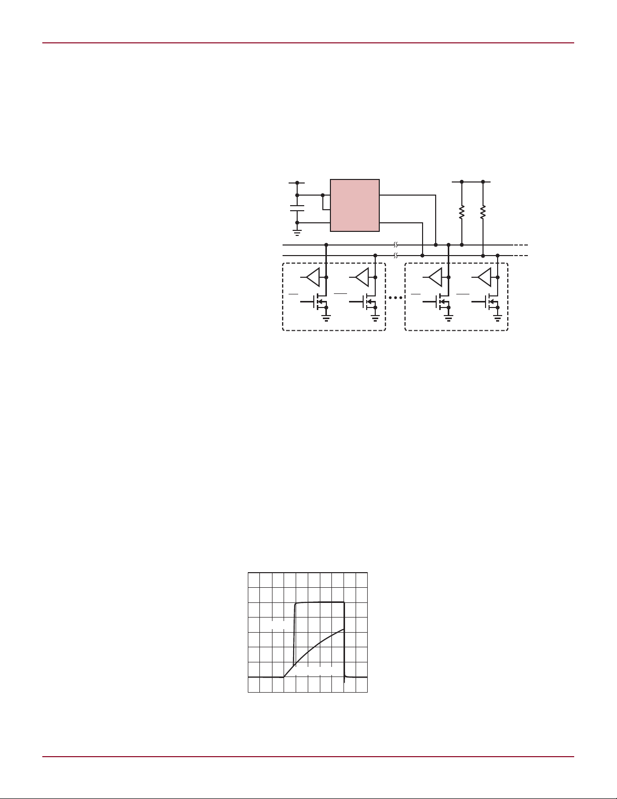
Figure 1 shows a typical low volt‑
age application circuit. The LTC4311
8
provides strong slew rate controlled
pull‑up currents on the bus for
smooth, controlled transitions during
rising edges to decrease rise times in
highly capacitive systems, as shown
in Figure 2. The LTC4311’s slew rate
controlled pull‑up currents are strong
enough to allow I2C or SMBus systems
to achieve switching frequencies up
to 400kHz for bus capacitances in
excess of 1nF. In addition, because
the accelerator pull‑up impedance
is significantly lower than the bus
pull‑up resistance, the system has
greater immunity to noise on rising
edges.
Figure 2. Comparison of I2C waveform
for the LTC4311 vs resistive pull-up
Figure 1. Typical LTC4311 low voltage application circuit
by Sam Tran
The LTC4311’s strong pull‑up cur‑
rents allow users to choose larger bus
pull‑up resistor values to reduce VOL,
DC bus power consumption and fall
times, while still meeting rise time and
switching frequency requirements.
This is especially helpful for 2‑wire
systems where devices require resis‑
tances in series with their pull‑down
devices for ESD protection, since
VOL on these devices is reduced with
larger bus pull‑up resistor values. The
larger bus pull‑up resistor values are
also beneficial in systems operating
at bus supplies below 2.7V, where
VOL can be reduced well below the
I2C specification, thereby increasing
noise margins.
For I2C or SMBus systems where
large numbers of I/O cards can be
inserted and removed, the LTC4311’s
slew rate controlled pull‑up currents
properly address rise time issues
despite large variations in bus ca‑
pacitance. The controlled slew rate
regulates the rise rate of the bus to
50V/µs–100V/µs, independent of bus
capacitance.
With very light loads, as occurs
when some or all cards are removed,
no reflections occur on the bus due
Linear Technology Magazine • March 2008
to the slew rate controlled nature of
–
+
–
+
–
+
–
+
–
+
V
THR
SLEW RATE
DETECTOR
CONTROL
LOGIC AND
INTERNAL SLEW
COMPARATOR
V
THR
V
CC
– 0.4
V
CC
– 0.4
1V
SLEW RATE
DETECTOR
5mA
BUS1 V
CC
GND
BUS2
ENABLE
5mA
LTC4311
V
CC
ENABLE
GND
V
CC
2.5V
C1
0.01µF
BUS1
BUS2
DEVICE 1
CLK
IN
CLK
OUT
V
CC
2.5V
DATA
IN
DATA
OUT
DEVICE N
CLK
IN
R2
10k
CLK
OUT
DATA
IN
DATA
OUT
R1
10k
OFF ON
I2C
SCL
SDA
the pull‑up currents. When the bus is
heavily loaded, the LTC4311 provides
strong, controlled pull‑up currents
to significantly decrease rise times
on the bus for capacitive loads well
beyond 1nF.
All of these features, coupled with
high ±8kV HBM ESD ruggedness,
make the LTC4311 ideally suited, and
in many cases necessary, for I2C or
SMBus systems having large numbers
of removable I/O cards.
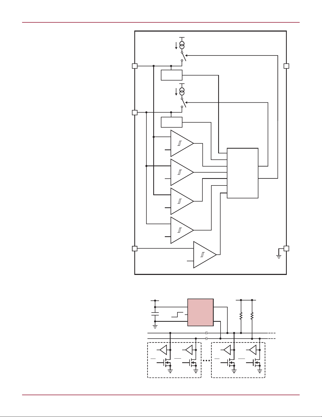
Circuit Operation
Figure 3 shows a functional block
diagram of the LTC4311. The LTC4311
consists of two independent but identi‑
cal circuits for each bus, consisting of
a slew rate detector, two voltage com‑
parators, and a slew rate controlled
bus pull‑up current.
The slew‑rate detector monitors
the bus and activates the accelerators
only when the bus rise rate is greater
than 0.2V/µs. This ensures that the
accelerators never turn on when the
bus voltage is in a DC state or falling.
The first voltage comparator is used to
hold off the accelerator until the bus
voltage exceeds a threshold voltage,
V
. For supply voltages below 2.7V,
THR
V
is supply dependent, defined as
THR
0.3 • VCC. At higher supply voltages,
V
is a constant 0.8V. This optimizes
THR
the LTC4311 for use in low voltage
systems, while offering rise time ac‑
celeration over a larger voltage range
for I2C and SMBus systems operating
at bus voltages above 2.7V.
Once both conditions are met, the
slew limited bus accelerator is enabled
to quickly slew the bus. An internal
slew rate comparator monitors the bus
rise rate and controls the accelerator
pull‑up current to limit the bus rise
rate to 50V/µs–100V/µs, independent
of the bus capacitance. A second volt‑
age comparator disables the pull‑up
current when the bus is within 400mV
of the bus pull‑up supply.
For systems where a single bus ac‑
celerator is not sufficient to meet the
rise time requirement, additional bus
accelerators can be added in parallel
to further decrease the rise time.
Linear Technology Magazine • March 2008
continued on page 23
Figure 4. Typical LTC4311 application with low current shutdown
DESIGN FEATURES L
Figure 3. LTC4311 functional block diagram
9

DESIGN FEATURES L
V V
mA
R
V V
A
S MAX
CC
S MIN( ) ( )
.−
≤ ≤
−5 7
5
7
250µ
comparators incorporate anti‑glitch
circuitry. Any transient at the input
of the monitor comparator must be
of sufficient magnitude and duration
(energy) to switch the comparator. De‑
signs utilizing these single supervisors
promote correct and glitch‑free resets,
which leads to stable and ultimately
more reliable systems.
Processor Communication
Two of the monitors (LTC2917 and
LTC2918) communicate with host
processors through their watchdog
circuits. The basic requirement for
the processor is to “pet” the watchdog
periodically to avoid being “bitten” by
the dog. Processor resets are invoked
by the built‑in watchdog hardware
when the watchdog petting frequency
has become too slow or too fast. Pre‑
cise knowledge of the system’s timing
characteristics is required to set the
watchdog timeout period. Adjust the
watchdog timeout period by connect‑
ing a capacitor between the watchdog
timing input (WT) and ground. Connect
WT to VCC to achieve a default 1.6s
timeout, without the need for external
capacitance.
Simple and Compliant Bias
A unique feature common to all four
of these devices is the ability to pro‑
vide operating bias from almost any
positive voltage. It does not matter
whether it is a 1.8V LDO, 5V switcher,
12V car battery, 24V wall‑wart or 48V
telecom supply; the integrated 6.2V
shunt regulator can work with any
system. For input voltages above 5.7V
the only requirement is to size the
bias resistor (RCC) to the range of the
input voltage. Connect RCC between
the high voltage supply and the VCC
input. Below 5.7V, simply connect
the supply directly to the VCC input.
Deriving resistor sizing for worst‑case
operation requires knowledge of the
minimum (V
(V
) input supply:
S(MAX)
) and maximum
S(MIN)
Be sure to decouple the VCC input
using a 0.1µF (or greater) capacitor
to ground.
Qualify Once, Specify Forever
During product development cycles,
power supply requirements often
change. While supply requirements
are changing, your choice of supervi‑
sor doesn’t have to. The LTC2915,
LTC2916, LTC2917 and LTC2918
can relieve the burden of having to
find the right supervisor for the job.
Qualify any one of these parts and you
can monitor any one of eight different
supply voltages, each with three dif‑
ferent internally fixed thresholds. You
can also monitor any custom voltage
down to 0.5V using an external resis‑
tor divider. Multi‑supply monitoring is
easily achieved by using two or more
devices and connecting their RST
outputs together.
Meet Your Match
The LTC2915, LTC2916, LTC2917 and
LTC2918 single supervisors are the
perfect match for a variety of applica‑
tions. Browse the applications shown
in the figures and quickly find the right
application for your system.
Conclusion
The LTC2915, LTC2916, LTC2917
and LTC2918 are feature‑laden single
supervisors that can be comfortably
placed near your monitored supply
and/or microprocessor, leading to
easy printed circuit board layout and
reliable system operation.
Unprecedented configurability
makes it possible to qualify and stock
just one product that can meet all of
your supervisory needs. Integration
provides twenty‑seven user‑select
able monitor thresholds with ±1.5%
accuracy. Any non‑standard thresh
old can be user‑configured with the
adjustable setting.
Other features include high volt‑
age operation, configurable reset and
watchdog timers, manual reset, and
low quiescent current. External com‑
ponents are seldom required to realize
fully functional designs. Electrical
specifications are guaranteed from
–40°C to 125°C.
L
‑
‑
LTC4311, continued from page 9
Auto Detect Standby Mode
and Disable Mode
To conserve power, when both bus
voltages are within 400mV of the bus
pull‑up supply, the LTC4311 enters
standby mode, consuming only 26µA
of supply current. When ENABLE
is forced low, as shown in Figure 4,
the LTC4311 enters a disable mode
and consumes less than 5µA of sup‑
ply current. Both bus pins are high
impedance when in disable mode or
when the LTC4311 is powered down,
regardless of the bus voltage.
Linear Technology Magazine • March 2008
Conclusion
The LTC4311 efficiently and effectively
addresses slow rise times, decreased
noise margins at low bus supplies, and
increased DC bus power consumption
found in 2‑wire bus systems. Strong
slew rate controlled pull‑up currents
quickly and smoothly slew the I2C
or SMBus bus lines, decreasing rise
times to allow up to 400kHz opera‑
tion for bus capacitances in excess
of 1nF. The advantages of the strong
slew rate controlled currents extend
to reducing the low state bus voltage,
DC bus power consumption, and fall
times, since larger value bus pull‑up
resistors can be used.
With a small 2mm × 2mm × 0.75mm
DFN or SC70 footprint, high ±8kV HBM
ESD performance and low power con‑
sumption in standby or disable mode,
the LTC4311 Low Voltage I2C or SMBus
accelerator is also ideally suited for
all I2C or SMBus systems. Examples
of such systems include notebooks,
palmtop computers, portable instru‑
ments, RAIDs, and servers where I/O
cards are hot‑swapped.
L
23
 Loading...