

LTC4309
Level Shifting Low Offset Hot
Swappable 2-Wire Bus Buffer
with Stuck Bus Recovery
FEATURES
n
Bidirectional Buffer Increases Fanout
n
60mV Buffer Offset Independent of Load
n
Optional Disconnect when Bus is Stuck Low
n
Prevents SDA and SCL Corruption During Live
Board Insertion and Removal from Backplane
n
Level Shift 2.5V, 3.3V and 5V Busses
n
Compatible with Non-Compliant VOL I2C Devices
n
±6kV Human Body Model ESD Ruggedness
n
Isolates Input SDA and SCL Lines from Output
n
Compatible with I2C™, I2C Fast-Mode and SMBus
n
READY Open Drain Output
n
FAULT Open Drain Output
n
1V Precharge on All SDA and SCL Lines
n
Optional Rise Time Accelerators
n
High Impedance SDA, SCL Pins for VCC = 0
n
Available in Small 12-Pin DFN (4mm x 3mm) and
16-Lead SSOP Packages
APPLICATIONS
n
Live Board Insertion
n
Servers
n
Capacitance Buffer/Bus Extender
n
RAID Systems
n
ATCA
DESCRIPTION
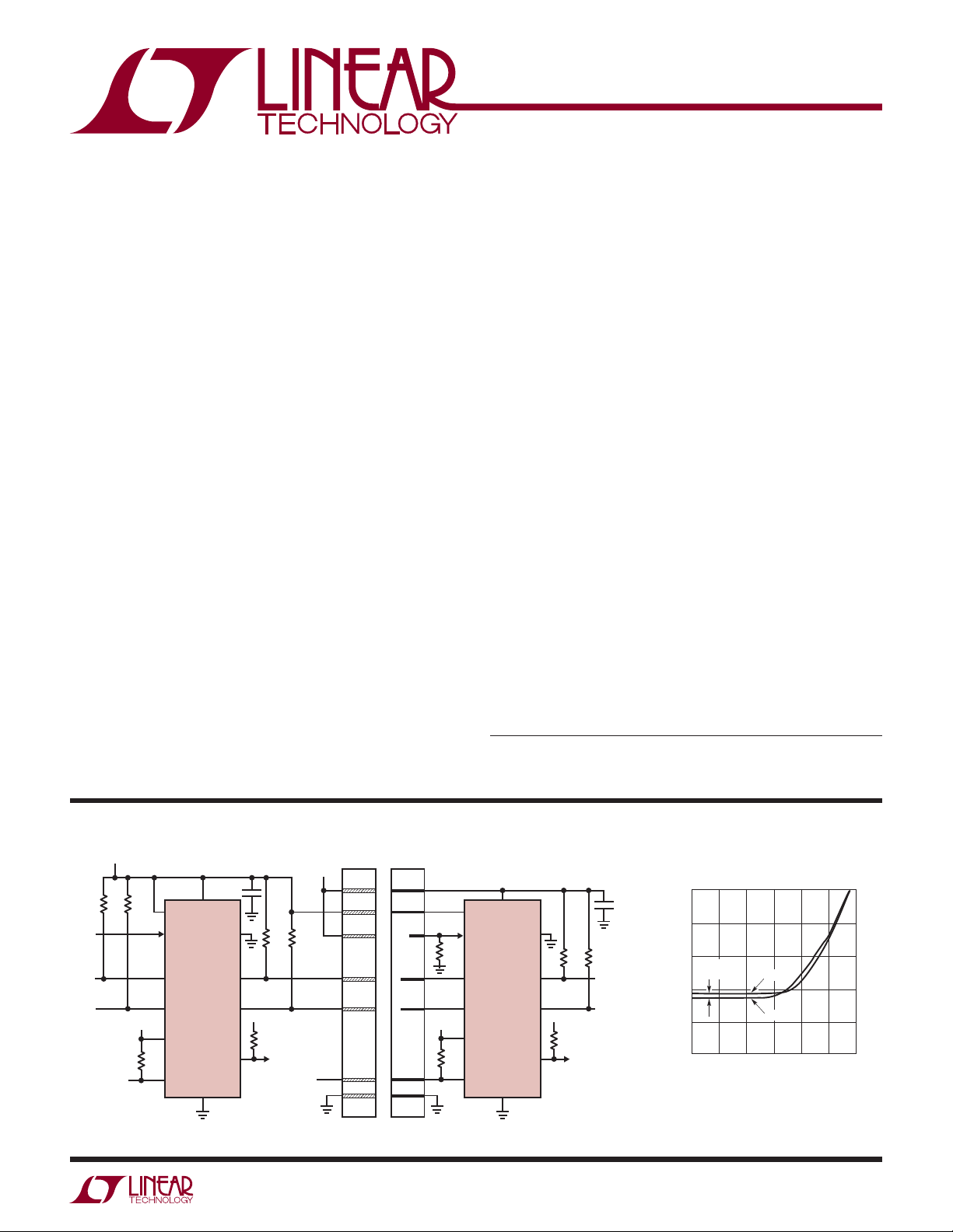
The LTC®4309 hot swappable 2-wire bus buffer allows
I/O card insertion into a live backplane without corruption of the data and clock busses. The LTC4309 provides
bidirectional buffering, keeping the backplane and card
capacitances isolated. Low offset and high VOL tolerance
allows cascading of multiple devices on the clock and data
busses. If SDAOUT or SCLOUT are low for 30ms, FAULT
will pull low indicating a stuck bus low condition. If DISCEN
is tied high, the LTC4309 will automatically break the bus
connection and generate up to 16 clock pulses and a stop
bit in an attempt to free the bus. A connection will resume
if the stuck bus is cleared. If DISCEN is connected to GND,
the busses will remain connected with no clock or stop
bit generation. ACC input enables rise-time accelerators
for high capacitively loaded busses.
During insertion, the SDA and SCL lines are precharged to
1V to minimize bus disturbances. When driven high, the
ENABLE input allows the LTC4309 to connect after a stop
bit or bus idle. Driving ENABLE low breaks the connection
between SDAIN and SDAOUT, SCLIN and SCLOUT. READY
is an open drain output which indicates that the backplane
and card sides are connected.
L, LT, LTC and LTM are registered trademarks of Linear Technology Corporation. All other
trademarks are the property of their respective owners. Protected by U.S. Patents including
6356140, 6650174, 7032051.
TYPICAL APPLICATION
3.3V
10k 10k
SCL1
SDA1
FAULT FAULT
V
ENABLEEN
SCLIN
SDAIN
3.3V
10k
FAULT
CC2
V
CC
LTC4309
GND
0.01μF
ACC
SCLOUT
SDAOUT
READY
2.7k 2.7k
3.3V
10k
5V
BACKPLANE
CONNECTOR
CARD
CONNECTOR
Rising Edge from Asserted Low
V
CC
V
CC2
ENABLE
100k
SCLIN
SDAIN
5V
DISCENDISCEN
10k
FAULT
LTC4309
GND
ACC
SCLOUT
SDAOUT
READY
10k 10k
5V
10k
0.01μF
SCL2
SDA2
4309 TA01
1000
200mV/DIV
800
600
400
200
0
LOW
OFFSET
0
200 300 400
100
SDAOUT
SDAIN
100ns/DIV
500 600
4309 G01
4309fa
1
LTC4309
T
ABSOLUTE MAXIMUM RATINGS
VCC, V
SDAIN, SCLIN, SDAOUT, SCLOUT,
ENABLE, FAULT, ACC, DISCEN .......................–0.3 to 6V
Maximum Sink Current (SDA, SCL, FAULT, READY)
I
SINK
to GND ............................................–0.3 to 6V
CC2
READY,
......................................................................50mA
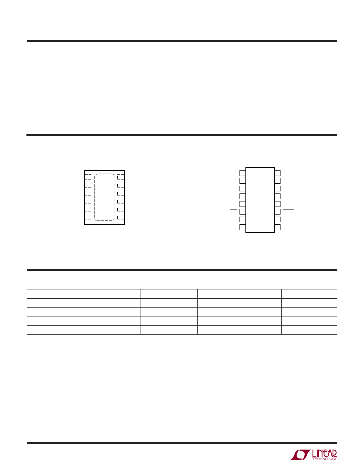
PIN CONFIGURATION
TOP VIEW
ENABLE
SCLOUT
EXPOSED PAD (PIN 13) PCB CONNECTION TO GND IS OPTIONAL
1
DISCEN
2
3
SCLIN
4
ACC
5
GND
6
12-LEAD (4mm × 3mm) PLASTIC DFN
DE12 PACKAGE
T
= 125°C, θJA = 43°C/W
JMAX
12
V
CC
V
11
CC2
SDAOUT
10
13
9
8
7
SDAIN
FAULT
READY
(Note 1, 6)
Operating Temperature
LTC4309C ................................................ 0°C to 70°C
LTC4309I.............................................. –40°C to 85°C
Storage Temperature Range (DE)........... –65°C to 125°C
Storage Temperature Range (GN) .......... –65°C to 150°C
Lead Temperature (Soldering, 10 sec)
GN Package ......................................................300°C
TOP VIEW
ENABLE
DISCEN
SCLOUT
1
2
NC
3
4
5
SCLIN
6
ACC
7
NC
8
GND
GN PACKAGE
16-LEAD NARROW PLASTIC SSOP
T
= 150°C, θJA = 110°C/W
JMAX
V
16
CC
NC
15
V
14
CC2
SDAOU
13
SDAIN
12
FAULT
11
NC
10
READY
9
ORDER INFORMATION
LEAD FREE FINISH TAPE AND REEL PART MARKING* PACKAGE DESCRIPTION TEMPERATURE RANGE
LTC4309CDE#PBF LTC4309CDE#TRPBF 4309 12-Lead (4mm × 3mm) Plastic DFN 0°C to 70°C
LTC4309IDE#PBF LTC4309IDE#TRPBF 4309 12-Lead (4mm × 3mm) Plastic DFN –40°C to 85°C
LTC4309CGN#PBF LTC4309CGN#TRPBF 4309 16-Lead Plastic SSOP 0°C to 70°C
LTC4309IGN#PBF LTC4309IGN#TRPBF 4309I 16-Lead Plastic SSOP –40°C to 85°C
Consult LTC Marketing for parts specifi ed with wider operating temperature ranges. *The temperature grade is identifi ed by a label on the shipping container.
Consult LTC Marketing for information on non-standard lead based fi nish parts.
For more information on lead free part marking, go to: http://www.linear.com/leadfree/
For more information on tape and reel specifi cations, go to: http://www.linear.com/tapeandreel/
4309fa
2
LTC4309
ELECTRICAL CHARACTERISTICS
The l denotes the specifi cations which apply over the full operating
temperature range, otherwise specifi cations are at T
SYMBOL PARAMETER CONDITIONS MIN TYP MAX UNITS
V
CC
V
CC2
I
CC
I
SD
I
CC2
I
SD2
Propagation Delay and Rise Time Accelerators
t
PHL
t
PLH
t
RISE
t
FALL
I
PULLUPAC
Start-Up Circuitry
V
PRE
t
IDLE
V
THR_EN
V
THR_EN(HYST)
V
THR_CTRL
I
CTRL
t
PLH_EN
t
PHL_EN
t
PLH_READY
t
PHL_READY
V
OL_READY
I
OFF_READY
Timing Characteristics
f
I2C, MAX
t
BUF
t
HD, STA
t
SU, STA
t
SU, STO
t
HD, DATI
t
SU, DAT
Input-Output Connection
V
OS
V
THR
Positive Supply Voltage
Input Side Accelerator Supply Voltage
VCC Input Supply Current Enabled VCC = V
V
Input Supply Current Disabled VCC = V
CC
V
Input Supply Current Enabled VCC = V
CC2
V
Input Supply Current Disabled VCC = V
CC2
SDA/SCL Propagation Delay High to Low C
SDA/SCL Propagation Delay Low to High C
SDA/SCL Rise Time C
SDA/SCL Fall Time C
Transient Boosted Pull-up Current Positive Transition > 0.8V/μS on SDA, SCL, VCC = 3.3V (Note 7) 5 8 mA
Precharge Voltage SDA, SCL Open
Bus Idle Time
ENABLE Threshold Voltage ENABLE Rising Edge
ENABLE Threshold Voltage Hysteresis (Note 3) 100 mV
ACC, DISCEN Threshold Voltage 0.5 0.7 1 V
ENABLE, ACC, DISCEN Input Currents ENABLE, ACC, DISCEN from 0 to V
ENABLE Delay Off-On (Figure 1) 95 μs
ENABLE Delay On-Off (Note 3), (Figure 1) 10 ns
READY Delay On-Off (Note 3), (Figure 1) 10 ns
READY Delay Off-On (Note 3), (Figure 1) 10 ns
READY Output Low Voltage I
READY Off Leakage Current VCC = READY = 5.5V
I2C Maximum Operating Frequency (Note 3) 400 600 kHz
Bus Free Time Between Stop and Start
Condition
Hold Time After (Repeated)
Start Condition
Repeated Start Condition Set-Up Time (Note 3) 0 ns
Stop Condition Set-Up Time (Note 3) 0 ns
Data Hold Time Input (Note 3) 0 ns
Data Set-Up Time (Note 3) 100 ns
Input-Output Offset Voltage 2.7k to V
SDA, SCL Logic Input Threshold Voltage VCC ≥ 2.9V
= 25°C. VCC = 3.3V, V
A
= 5.5V, V
CC2
= 5.5V, SDA = SCL = 5.5V, ENABLE = OV
CC2
= 5.5V, V
CC2
= 5.5V, SDA = SCL = 5.5V, ENABLE = OV
CC2
= 50pF, 2.7k to VCC on SDA, SCL, (Note 3, 4), (Figure 1) 85 ns
LOAD
= 50pF, 2.7k to VCC on SDA, SCL, (Note 3, 4), (Figure 1) 10 ns
LOAD
= 100pF, 10k to VCC on SDA, SCL, VCC = 5V V
LOAD
SDAIN
SDAIN
= 3.3V, unless otherwise noted.
CC2
= V
= V
= 0V (Note 2)
SCLIN
= 0V (Note 2)
SCLIN
CC2
= 5V,
l
2.3 5.5 V
l
1.8 5.5 V
l
l
l
l
711 mA
900 1400 μA
190 250 μA
140 180 μA
30 300 ns
(Note 3, 5), (Figure 1)
= 100pF, 10k to VCC on SDA, SCL, VCC = 5V (Note 3, 5),
LOAD
30 300 ns
(Figure 1)
l
0.8 1.0 1.2 V
l
55 95 175 μs
l
0.8 1.4 2 V
= 3mA, VCC = 2.3V
READY
CC
l
l
l
0.1 ±5 μA
0.4 V
0.1 ±5 μA
(Note 3) 1.3 μs
(Note 3) 100 ns
l
20 60 100 mV
1.4
1.65
1.1
1.35
1.9
1.6
V
CC
< 2.9V
on SDA, SCL, Driven SDA, SCL = 0.2V
CC2
V
V
4309fa
3
LTC4309
The l denotes the specifi cations which apply over the full operating
ELECTRICAL CHARACTERISTICS
temperature range, otherwise specifi cations are at T
SYMBOL PARAMETER CONDITIONS MIN TYP MAX UNITS
V
THR(HYST)
C
IN
I
LEAK
V
OL
V
ILMAX
Bus Stuck Low Timeout
t
TIMEOUT
V
OL_FAULT
I
OFF_FAULT
Note 1: Stresses beyond those listed under Absolute Maximum Ratings
may cause permanent damage to the device. Exposure to any Absolute
Maximum Rating condition for extended periods may affect device
reliability and lifetime.
Note 2: Test performed with connection circuity active.
Note 3: Determined by design, not subject to test.
Note 4: For larger equivalent bus capacitance, the skew increases, and
SDA, SCL Logic Input Threshold Voltage
Hysteresis
Digital Input Capacitance SDAIN,
SDAOUT, SCLIN, SCLOUT
Input Leakage Current SDA, SCL, ACC, DISCEN Pins
Output Low Voltage SDA, SCL Pins, I
Buffer Input Logic Low Voltage
Bus Stuck Low Timer SDAOUT, SCLOUT = OV
FAULT Output Low Voltage I
FAULT Off Leakage Current
= 25°C. VCC = 3.3V, V
A
= 3.3V, unless otherwise noted.
CC2
(Note 3) 50 mV
(Note 3) 10 pF
V
= 2.7V
CC2
2.7k to V
V
= V
CC
= 3mA
FAULT
= 4mA, Driven SDA/SCL = 0.2V, VCC =
SINK
on SDA, SCL, Driven SDA/SCL = 0.1V,
CC
= 3.3V
CC2
l
l
0 0.4 V
l
120 170 205 mV
l
l
25 30 35 ms
l
l
±5 μA
1.2 V
0.4 V
0.1 ±5 μA
setup and hold times must be adjusted accordingly. Please see the
Operation Section of the datasheet.
Note 5: Measure points are 0.3 • V
and 0.7 • VCC.
CC
Note 6: All currents into pins are positive, all voltages are referenced to
GND, unless otherwise specifi ed.
Note 7: I
varies with temperature and VCC voltage as shown in the
PULLUPAC
Typical Performance Characteristics section.
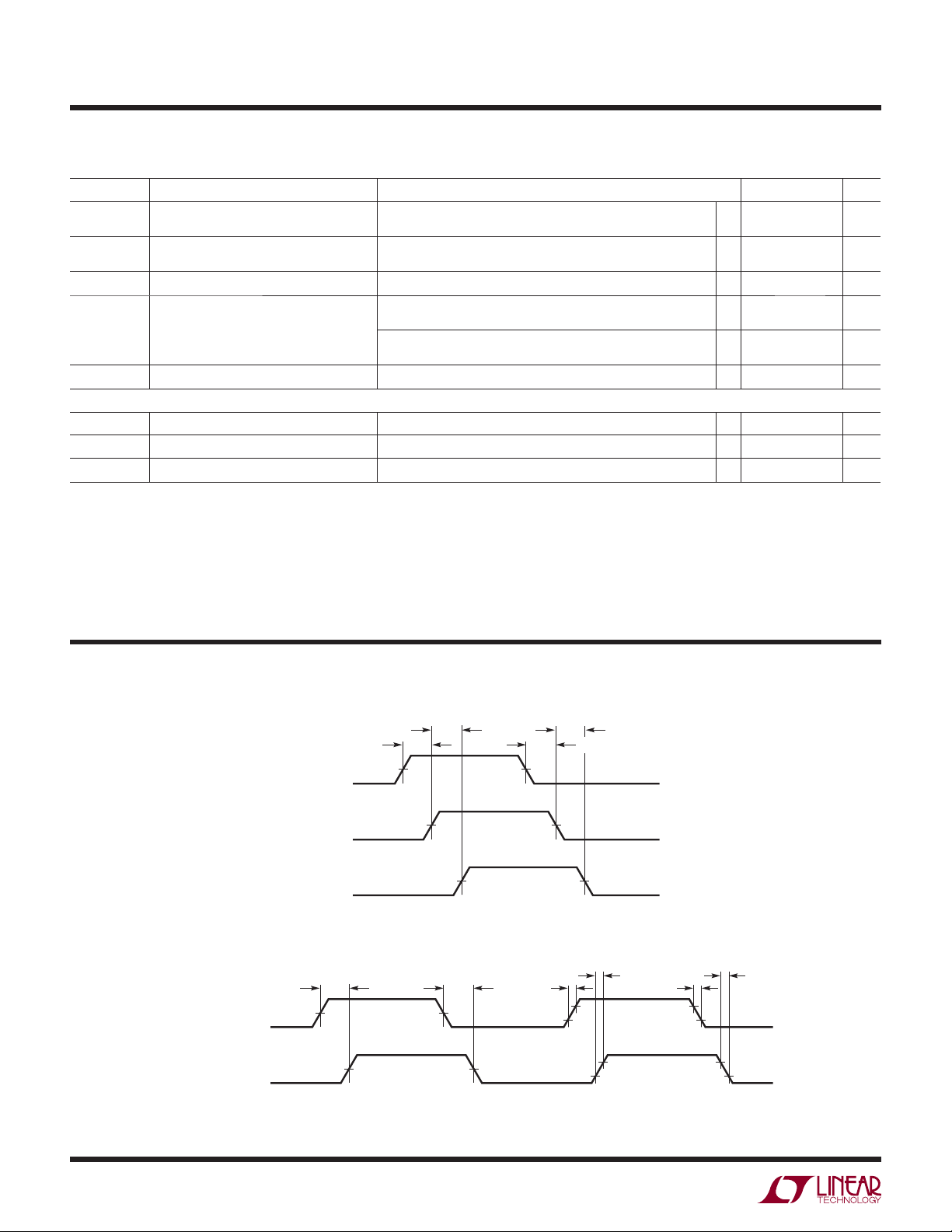
TIMING DIAGRAMS
SDAIN/SCLIN
SDAOUT/SCLOUT
ENABLE and READY Timing
t
PLH_READY
t
PLH_EN
ENABLE
CONNECT
READY
SDA/SCL Propagation Delays, Rise and Fall Times
t
PLH
t
PHLtRISE
Figure 1. Timing Diagrams
t
PHL_EN
t
PHL_READY
4309 TD01
t
RISE
t
FALL
t
FALL
4309 TD02
4
4309fa
LTC4309
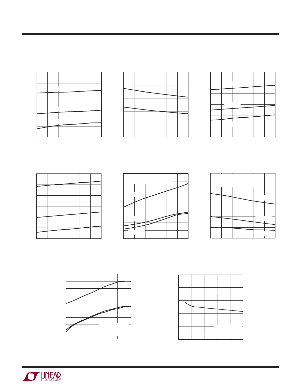
TYPICAL PERFORMANCE CHARACTERISTICS
T
= 25°C, VCC = 3.3V, V
A
otherwise noted.
ICC Enabled Current vs
Temperature
8
7.5
VCC = 5.5V
7
6.5
6
ENABLED CURRENT (mA)
CC
I
5.5
5
–50
VCC = 3.3V
VCC = 2.3V
–25 0 50
TEMPERATURE (oC)
I
Disabled Current vs
CC2
Temperature
160
140
130
120
110
SUPPLY CURRENT (MA)
100
90
–50
VCC = 5.5V
VCC = 3.3V
VCC = 2.3V
02550
–25
TEMPERATURE (oC)
100
25
75
4309 G02
75 100
4309 G05
ICC Disabled Current vs
Temperature
20
16
12
(mA)
8
PULLUPAC
I
4
0
–50
–25
VCC = 5.5V
VCC = 3.3V
25 50
0
TEMPERATURE (°C)
Input-Output High to Low
Propagation Delay vs Temperature
140
CIN = C
R
130
120
110
100
90
80
PROPAGATION DELAY (ns)
70
60
–50
= 50pF
OUT
= R
PULLUPIN
VCC= 5.5V
VCC= 2.3V
VCC= 3.3V
–25 0 25 100
TEMPERATURE (°C)
PULLUPOUT
= 2.7kΩ
50 75
220
200
180
160
140
SUPPLY CURRENT (MA)
120
100
75
100
4309 G03
4309 G06
–50
30
25
20
15
10
5
BOOST PULL-UP CURRENT (mA)
0
–50
= 3.3V unless
CC2
I
Enabled Current vs
CC2
Temperature
VCC = 5.5V
VCC = 3.3V
VCC = 2.3V
–25
25 50
0
TEMPERATURE (oC)
Boost Pull-Up Current vs
Temperature
CIN = 50pF
C
= 1nF
OUT
= R
R
PULLUPIN
PULLUPOUT
–25 0 25 100
TEMPERATURE (°C)
= 2.7kΩ
VCC= 3.3V
50 75
75
4309 G04
VCC= 5.5V
VCC= 2.3V
4309 G07
100
Input-Output High to Low Propagation
Delay vs Output Capacitance
160
150
140
VCC= 5.5V
130
120
110
VCC= 2.3V
100
PROPAGATION DELAY (ns)
90
VCC= 3.3V
80
70
200 400 600 800
0
OUTPUT CAPACITANCE (pF)
CIN = 50pF
R
PULLUPIN
R
PULLUPOUT
= 2.7k7
= 2.7k7
4309 G08
1000
Offset Voltage vs Pull-Up
Resistance
70
66
62
58
OFFSET VOLTAGE (mV)
54
50
0
46
2
PULL-UP RESISTANCE (kΩ)
VOL = 0.1V
C
IN = COUT
R
PULLUPIN
= 50pF
= 2.7kΩ
8
4309 G09
10
4309fa
5

LTC4309
PIN FUNCTIONS
(DE12/GN16)
ENABLE (Pin 1/Pin1): Connection Enable Input. This 1.4V
digital threshold input pin enables or disables the LTC4309.
For normal operation pull or connect ENABLE high. Driving
ENABLE below the 0.8V threshold isolates SDAIN from
SDAOUT, SCLIN from SCLOUT, asserts READY low, and
prohibits automatic clock and stop bit generation during a
fault condition. A rising edge on ENABLE after a fault has
occurred forces a connection between SDAIN, SDAOUT
and SCLIN, SCLOUT. Connect to V
if unused.
CC
DISCEN (Pin 2/Pin 3 ): Bus Stuck Low Disconnect Enable
Input. This pin, when high, allows the stuck low bus
timeout circuitry to disconnect the bus in a fault condition.
When connected to GND, this pin disables the circuitry
that disconnects the bus under a fault condition; however,
the FAULT pin will still go low.
SCLOUT (Pin 3/Pin 4): Serial Clock Output. Connect this
pin to a SCL bus segment where bus stuck low recovery is
desired. If the output rise time accelerators are enabled, a
pull-up resistor should be connected between this pin and
a bus supply greater than or equal to V
can be lower than V
if the output rise time accelerators
CC
. Bus supplies
CC
are disabled. See Application Information section for
detailed bus pull-up supply options.
SCLIN (Pin 4/Pin 5): Serial Clock Input. Connect this pin
to a SCL bus segment where isolation from bus stuck
low issues is desired. If the input rise time accelerator is
enabled, a pull-up resistor should be connected between
this pin and a bus supply greater than or equal to V
Bus supplies can be lower than V
if the input rise time
CC2
CC2
.
accelerators are disabled. See Application Information
section for detailed bus pull-up supply options.
ACC (Pin 5/Pin 6): Rise Time Accelerator Control Input.
This nominal 0.7V threshold input pin enables and disables
all rise time accelerators on the SDA and SCL pins. Connect
ACC to GND to enable all four rise time accelerators or
connect ACC to V
Connect ACC to V
to disable all four rise time accelerators.
CC
to GND to enable the accelerators
CC2
on SDAOUT and SCLOUT only.
GND (Pin 6/Pin 8): Device Ground. Connect this pin to a
ground plane for best results.
READY (Pin 7/Pin 9): Connection Ready Status Output.
This open-drain N-channel MOSFET pin pulls low when
ENABLE is low, when the start-up and connection sequence
described in the Operation section has not been completed,
or when the LTC4309 disconnects the input and output
pins due to a bus stuck low condition. READY goes high
when ENABLE is high and connection is made between the
input and output pins. Connect a pull-up resistor, typically
10k, from this pin to the bus pull-up supply. This pin can
be left open if unused.
FAUL T (Pin 8/Pin 11): Bus Stuck Low Timeout Output. This
open drain N-channel MOSFET output pulls low after 30ms
when there is a bus stuck low condition on the output pins
of the LTC4309. In normal operation FAUL T is high. Connect
a pull-up resistor, typically 10k, from this pin to the bus
pull-up supply. This pin can be left open if unused.
SDAIN (Pin 9/Pin 12): Serial Clock Input. Connect this
pin to a SDA bus segment where isolation from bus stuck
low issues is desired. If the input accelerator is enabled, a
pull-up resistor should be connected between this pin and
a bus supply greater than or equal to V
can be lower than V
if the input rise time accelerators
CC2
. Bus supplies
CC2
are disabled. See Application Information section for
detailed bus pull-up supply options.
SDAOUT (Pin 10/Pin 13): Serial Clock Output. Connect this
pin to a SCL bus segment where bus stuck low recovery is
desired. If the output rise time accelerators are enabled, a
pull-up resistor should be connected between this pin and
a bus supply greater than or equal to V
can be lower than V
if the output rise time accelerators
CC
. Bus supplies
CC
are disabled. See Application Information section for
detailed bus pull-up supply options.
(Pin 11/Pin 14): Supply Voltage Input for SDAIN and
V
CC2
SCLIN Rise Time Accelerator Circuitry. V
supplies the
CC2
rise time accelerator circuitry on the input side. Bypass
this pin to GND with a capacitor of at least 0.01μF and
place close to V
for best results. If V
CC2
is connected
CC2
to GND, the input side rise time accelerator circuitry is
disabled, regardless of ACC.
4309fa
6

LTC4309
PIN FUNCTIONS
(DE12/GN16)
VCC (Pin 12/Pin 16): Supply Voltage Input. Bypass this
pin to GND with a capacitor of at least 0.01μF and place
close to V
for best results.
CC
BLOCK DIAGRAM
V
V
CC2
SDAIN
SCLIN
100k
100k
SLEW RATE
DETECTOR
8mA
8mA
CC2
I
BOOSTSDA
PRECHARGE
V
CC2
PC
CONNECT
I
BOOSTSCL
EXPOSED PAD (Pin 13 DE12 Package Only): Exposed Pad
may be left open or connected to device ground.
V
CC
V
CC
SDAOUT
SCLOUT
CONNECT
PC
CONNECT
CONNECT
I
BOOSTSDA
SLEW RATE
I
BOOSTSCL
DETECTOR
8mA
100k
V
CC
8mA
100k
ACC
DISCEN
ENABLE
4309 BD
SLEW RATE
DETECTOR
1.65V/1.6V
1.35V/1.3V
1.65V/1.6V
1.35V/1.3V
1.4V/1.3V
SLEW RATE
DETECTOR
+
1.65V/1.6V
30ms
TIMER
–
1.35V/1.3V
+
1.65V/1.6V
–
1.35V/1.3V
I
+
LOGIC
–
+
–
BOOSTSCL
I
BOOSTSDA
PC CONNECT
CONNECT
FAULT
READY
+
–
95μs
UVLO
DELAY
CONNECT
GND
4309fa
7

LTC4309
OPERATION
Start-Up
When the LTC4309 fi rst receives power on its V
either during power up or live insertion, it starts in an under
voltage lockout (UVLO) state, ignoring any activity on the
SDA or SCL pins until V
the LTC4309 does not try to function until enough supply
voltage is present.
During this time, the 1V precharge circuitry is actively
forcing 1V through 100k nominal resistors to the SDA
and SCL pins. Because the I/O card is being plugged
into a live backplane, the voltage on the backplane SDA
and SCL busses may be anywhere between 0V and V
Precharging the SCL and SDA pins to 1V minimizes the
worst-case voltage differential these pins will see at the
moment of contact, therefore minimizing the amount of
disturbance caused by the I/O card.
Once the LTC4309 exits from UVLO, it monitors both the
input and output pins for either a stop bit or a bus idle
condition to indicate the completion of data transactions.
When both sides are idle or one side has a stop bit while
the other is idle, the connection circuitry is activated,
joining the SDA and SCL busses on the input side with
those on the output side.
Rise Time Accelerators
Once connection has been established if ACC is connected
to ground and V
than or equal to 1.8V, the rise time accelerator circuits on
all four SDA and SCL pins are enabled. During positive bus
transitions of at least 0.8V/μs, the rise time accelerators
provide strong, slew-limited pull-up currents to force the
bus voltage to rise at a rate of 100V/μs. Enabling the rise
time accelerators allows users to choose larger bus pullup resistors, reducing power consumption and improving
logic low noise margins, or design with bus capacitances
beyond those specifi ed in the I
To ensure the rise time accelerators are properly activated
when the rise time accelerators are enabled, users should
choose bus pull-up resistors that guarantee the bus will
rise on its own at a rate of at least 0.8V/μs. See the Application Information section for determining the correct
pull-up resistor size.
is powered from a supply voltage greater
CC2
rises above 2V. This ensures
CC
2
C specifi cations.
CC
pin,
.
CC
All four rise time accelerators can be disabled by connecting ACC to V
only SDAOUT and SCLOUT, connect both ACC and V
to ground. The rise time accelerators are also internally
disabled until the sequence of events described in the
start-up section have been completed, as well as during
automatic clocking and stop bit generation for a bus stuck
low recovery event.
Connection Circuitry
Once the connection circuitry is activated, the functionality
of the input and output bus of the respective SDA or SCL
pins are identical. A low forced on either output or input
pin at any time results in both pin voltages forced low.
The LTC4309 is tolerant of I
up to the V
When the LTC4309 senses a rising edge on the bus, with
a slew rate greater than 0.8V/μs, the internal pull-down
device for the respective bus is deactivated at bus voltages as low as 0.48V. This methodology maximizes the
effectiveness of the rise time accelerator circuitry and
maintains compatibility with other devices in the LTC4300
bus buffer family. Care must be taken to ensure devices
participating in clock stretching or arbitration are capable
of forcing logic low voltages below 0.48V at the LTC4309’s
SDA and SCL pins.
A high occurs when all devices on the input and output
pins release high. These important features ensures the
2
C specifi cation protocols such as clock stretching, clock
I
synchronization, arbitration, and acknowledge function
seamlessly in all cases as specifi ed, regardless of how the
devices in the system are connected to the LTC4309.
Another key feature provided by the connection circuitry
is input and output bus capacitance isolation through
bidirectional buffering. Because of this isolation, the
waveforms on the input busses look slightly different than
the corresponding output bus waveforms, as described
below.
Input to Output Offset Voltage
When a logic low voltage is driven on any of the LTC4309’s
data or clock pins, the LTC4309 regulates the voltage on
the other side of the device to a slightly higher voltage,
. To activate the rise time accelerators on
CC
2
C bus DC logic low voltages
specifi cation of 0.3 • VCC.
IL
CC2
4309fa
8

OPERATION
LTC4309
OUTPUT SIDE
50pF
1V/DIV
200ns/DIV
Figure 2. Input-Output Rising Edge Waveforms
INPUT SIDE
150pF
1V/DIV
4307 F01
typically 60mV. This offset is nearly independent of pull-up
current. (See Typical Performance curves.)
Propagation Delays
During a rising edge, the rise time on each side is determined by the bus pull-up resistor and the equivalent
capacitance on the line. If the pull-up resistors are the
same, a difference in rise time occurs which is directly
proportional to the difference in capacitance between the
two sides. This effect is displayed in Figure 2 for V
= 5.5V and a 10k pull-up resistor on each side (50pF
V
CC2
CC
and
on one side and 150pF on the other). Since the output side
has less capacitance than the input, it rises faster and the
effective propagation delay is negative.
There is a fi nite propagation delay through the connection circuitry for falling waveforms. Figure 3 shows the
falling edge waveforms for the same pull-up resistors and
equivalent capacitance conditions as used in Figure 2. An
external N-channel MOSFET device pulls down the voltage
on the side with 150pF capacitance; LTC4309 pulls down
the voltage on the opposite side, with a delay of 85ns. This
delay is always positive and is a function of supply voltage,
temperature and the pull-up resistors and equivalent bus
capacitances on both sides of the bus.
The Typical Performance Characteristics section shows
Propagation Delay as a function of temperature and voltage
for 2.7k pull-up resistors and 50pF equivalent capacitance
on both sides of the part. Also, the Propagation Delay as
a function of Output Capacitance curve shows that larger
output capacitances translate to longer delays. Users must
quantify the difference in propagation times for a rising
edge versus a falling edge in their systems and adjust
setup and hold times accordingly.
INPUT SIDE
150pF
1V/DIV
200ns/DIV
Figure 3. Input-Output Falling Edge Waveforms
OUTPUT SIDE
50pF
1V/DIV
4307 F02
Bus Stuck Low Timeout
When SDAOUT or SCLOUT is low, an internal timer is
started. The timer is only reset by the respective pin
going high. If the bus stuck low does not go high within
30ms (typical), the FAULT pin pulls low indicating a bus
stuck low condition. If DISCEN is connected to V
CC
, the
connection circuitry is disabled, breaking the connection
between the respective input and output pins. In addition,
after at least 40μs, up to 16 clock pulses at 8.5kHz (typical) is generated on the SCLOUT pin by the LTC4309 in an
attempt to free the stuck low bus. Once the clock pulses
have completed, a stop bit is generated on the SCLOUT
and SDAOUT pins to reset all devices on the bus.
If the stuck low SDAOUT or SCLOUT recovers to a logic
high, the FAULT flag clears, and the LTC4309 waits for
either a stop bit or a bus idle condition to activate the
connection circuitry to reconnect the input and output
busses.
If DISCEN is connected to GND, the FAULT pin will pull
low, but the connection circuitry will not be disabled,
leaving the input and output busses connected. Also, no
clock or stop bit is generated.
When powering up into a bus stuck low condition, the
connection circuitry connecting the SDA and SCL busses
on the I/O card with those on the backplane is not activated.
30ms after UVLO, the FAULT pin pulls low indicating a bus
stuck low condition and automatic clocking and stop bit
generation takes place as described above.
READY Digital Output
This pin provides a digital fl ag which is low when either
ENABLE is low, the start-up sequence described earlier
in this section has not been completed, or the LTC4309
4309fa
9

LTC4309
OPERATION
has disconnected the input and output busses due to a
bus stuck low condition. READY goes high when ENABLE
is high and start-up is complete. The pin is driven by an
open drain pull-down device capable of sinking 3mA
while holding 0.4V on the pin. Connect a resistor to the
bus pull-up supply to provide the pull-up.
FAULT Digital Output
This pin provides a digital flag which is low when SDA
or SCL is low for 30ms (typical). The pin is driven by an
open drain pull-down capable of sinking 3mA while holding 0.4V on the pin. Connect a resistor from FAULT to the
bus pull-up supply to provide the pull-up.
APPLICATIONS INFORMATION
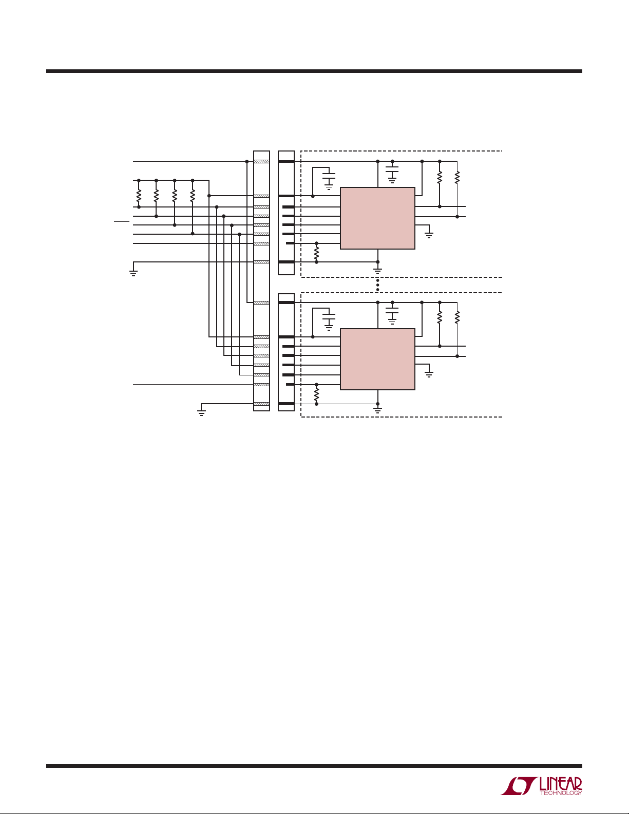
Live Insertion and Capacitance Buffering Application
Figures 4 and 5 illustrate applications of the LTC4309 that
TM
take advantage of the LTC4309’s Hot Swap
buffering and precharge features. If the I/O cards were
plugged directly into the backplane without the LTC4309
buffer, all of the backplane and card capacitances would
add directly together, making rise time and fall time requirements difficult to meet. Placing an LTC4309 on the
edge of each card, however, isolates the card capacitance
from the backplane. For a given I/O card, the LTC4309
drives the capacitance of everything on the card and the
backplane must drive only the capacitance of the LTC4309,
which is less than 10pF.
Figure 4 shows the LTC4309 used in the typical staggered
connector application, where V
“early power” pins. The “early power” pins ensure the
LTC4309 is initially powered and forcing a 1V precharge
voltage on the medium length SDA and SCL pins before
they contact to the backplane busses. Coupled with
ENABLE as the shortest pin, passively pulled to ground
by a resistor, the staggered approach provides additional
time for transients associated with live insertion to settle
before the LTC4309 can be enabled.
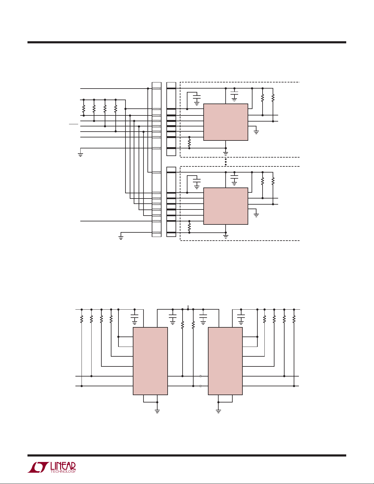
Figure 5 shows the LTC4309 in an application where all
of the pins have the same length. In this application, a
and GND are the longest
CC
, capacitance
ENABLE
When the ENABLE pin is driven below 0.8V with respect
to the LTC4309’s ground, the input pin is disconnected
from the output pin and the READY pin is internally pulled
low. When the pin is driven above 2V, the part waits for
data transactions on both the input and output pins to be
complete (as described in the Start-Up section) before
connecting the two sides. At this time the internal pulldown on READY releases.
A rising edge on ENABLE after a fault has occurred forces a
connection between SDAIN, SDAOUT and SCLIN, SCLOUT,
even if the bus stuck low conditions has not been cleared.
At this time, the 30ms timer is reset, but not disabled.
resistor is used to hold the ENABLE pin low during live
insertion, until the backplane control circuitry can enable
the device.
Repeater/Bus Extender Applications
Users who wish to connect two 2-wire systems separated
by a distance can do so by connecting two LTC4309s backto-back, as shown in Figure 6. The I
for 400pF maximum bus capacitance, severely limiting
the length of the bus. The SMBus specification places no
restriction on bus capacitance, but the limited impedances
of devices connected to the bus require systems to remain
small if rise time and fall time specifications are to be met.
In this situation, the differential ground voltage between
the two systems may limit the allowed distance, because
a valid logic low voltage with respect to the ground at one
end of the system may violate the allowed V
with respect to the ground at the other end. In addition,
the connection circuitry offset voltages of the back-toback LTC4309s add together, directly contributing to the
same problem.
Figure 7 further illustrates a repeater application. In
AdvancedTCA applications, the bus pull-up resistance can
be quite small. Since there is no effect on the offset due
Hot Swap is a trademark of Linear Technology Corporation.
2
C specification allows
specification
OL
4309fa
10

APPLICATIONS INFORMATION
LTC4309
to the pull-up impedance, multiple LTC4309 buffers can
be used in a single system. This allows the user to divide
the line and device capacitances into more sections with
buffering and meet rise and fall times.
The LTC4309 disconnects when both bus I/O’s are above
0.48V and rising. In systems with large ground bounce,
if many devices are cascaded, the 0.48V threshold can be
exceeded, and the transients associated with the ground
bounce can appear to be a rising edge. Under this condition,
the LTC4309 with inputs above 0.48V may disconnect.
Level Shifting Applications
Systems requiring different supply voltages for the
backplane side and the card side can use the LTC4309
for bidirectional level shifting, as shown in Figure 6. The
LTC4309 can level shift between bus pull-up supplies as
low as 1.7V, with the accelerators disabled, to as high as
5.5V. Level shifting allows newer designs that require low
voltage supplies, such as EEPROMs and microcontrollers,
the capability to interface with legacy backplanes which
may be operating at higher supply voltages.
Systems with Supply Voltage Droop
In large 2-wire systems, the supply voltages seen by devices
at various points in the system can differ by a few hundred
millivolts or more. For proper operation, make sure that
the V
CC2(LTC4309)
is ≥ 1.8V, and V
CC(LTC4309)
≥ 2.3V.
Additional Pull-Up Supply Options
If the rise time accelerators are enabled, the bus pull-up
supply can be greater than or equal to V
for the output
CC
busses and accordingly, the input pull-up supply can
be greater than or equal to V
for the input busses.
CC2
This ensures the LTC4309’s rise time accelerators do
not source current through the pull-up resistors into the
pull-up supply. If the rise time accelerator circuitries are
disabled, the bus pull-up supply can be as low as 2V for
≥ 2.9V and for VCC < 2.9V, the bus pull-up supply can
V
CC
be as low as 1.7V. The bound on the lower supply limit
exists to ensure the bus signal range exceeds the logic
input threshold voltage, V
THR
.
Resistor Pull-Up Value Selection
To guarantee the rise time accelerators are activated during
a rising edge, the bus must rise on its own with a positive
slew rate of at least 0.8V/μs. To achieve this, choose a
maximum resistor value R
R
PULLUP
(V
BUS(MIN)
Where R
V
BUS(MIN)
C
BUS
PULLUP
is the equivalent bus capacitance in pico-Farads
is the pull-up resistor value in kilo ohms,
is the minimum bus pull-up supply voltage and
PULLUP
– 0.8V)• 1250
C
using the formula:
ns
V
BUS
(pF).
To estimate the value of C
, use a general rule of 20pF
BUS
of capacitance per device on the bus (10pF for the device
and 10pF for interconnect).
In typical applications, a pull-up resistor connected from
the LTC4309’s bus output pins to V
to V
or VCC, if V
CC2
is grounded, is suffi cient. However,
CC2
and bus input pins
CC
for unique applications, additional fl exibility is available for
bus pull-up supplies other than V
CC
or V
. One example
CC2
is shown in Figure 8. The expanded bus pull-up range is
dependent on the user confi guration of the rise time accelerators and the supply voltage, V
CC
.
In addition, R
PULLUP
must be strong enough to overcome
the precharge voltage and provide logic highs on SDAOUT
and SCLOUT for the start-up and connection circuitry to
connect the backplane to the card. Regardless of the bus
capacitance, always choose
V
BUS(MAX)–VTHR
100μA
4309fa
R
PULLUP
11
LTC4309
APPLICATIONS INFORMATION
V
SDA
SCL
FAULT
READY
ENA1
ENAN
BACKPLANE
V
CC
CC2
R1
10k
BACKPLANE
R2
10kR310kR410k
CONNECTOR
CARD
CONNECTORS
I/O PERIPHERAL CARD 1
C2
0.01μF
V
CC2
SDAIN
SCLIN
FAULT
READY
ENABLE
R7
10k
I/O PERIPHERAL CARD N
C4
0.01μF
V
CC2
SDAIN
SCLIN
FAULT
READY
ENABLE
R10
10k
V
CC
LTC4309
GND
V
CC
LTC4309
GND
C1
0.01μF
DISCEN
SDAOUT
SCLOUT
ACC
C3
0.01μF
DISCEN
SDAOUT
SCLOUT
ACC
R5
R6
10k
10k
R8
10kR910k
CARD 1_SDA
CARD 1_SCL
CARD N_SDA
CARD N_SCL
4309 F01
Figure 4. The LTC4309 in an Application with a Staggered Connector.
12
4309fa
APPLICATIONS INFORMATION
LTC4309
V
SDA
SCL
FAULT
READY
ENA1
ENAN
BACKPLANE
V
CC
CC2
R1
10k
BACKPLANE
R2
10kR310kR410k
CONNECTOR
CARD
CONNECTORS
I/O PERIPHERAL CARD 1
C2
0.01μF
V
CC2
SDAIN
SCLIN
FAULT
READY
ENABLE
R7
10k
I/O PERIPHERAL CARD N
C4
0.01μF
V
CC2
SDAIN
SCLIN
FAULT
READY
ENABLE
R10
10k
V
CC
LTC4309
GND
V
CC
LTC4309
GND
C1
0.01μF
DISCEN
SDAOUT
SCLOUT
ACC
C3
0.01μF
DISCEN
SDAOUT
SCLOUT
ACC
Figure 5. The LTC4309 in an Application Where All the Pins Have the Same Length.
R5
R6
10k
10k
R8
10kR910k
CARD 1_SDA
CARD 1_SCL
CARD N_SDA
CARD N_SCL
4309 F01
3.3V
SDA1
SCL1
10k
2.5V
R3
R2
R1
10k
10k
10k
R4
0.01μF
C1
V
CCVCC2
DISCEN
ENABLE
READY
FAULT
SDAOUT
SCLOUT
ACC ACC
LTC4309
GND
0.01μF
SDAIN
SCLIN
C2
R5
2.7k
R6
2.7k
C3
0.01μF
SDAIN
SCLIN
V
CC2
LTC4309
GND
V
CC
DISCEN
ENABLE
READY
FAULT
SDAOUT
SCLOUT
C4
0.01μF
R7
10k
R8
10kR910k
R10
10k
5V
SDA2
SCL2
4309 F04
Figure 6. The LTC4309 in a Level Shifting Repeater/Bus Extender Application.
4309fa
13

LTC4309
APPLICATIONS INFORMATION
V
SDA1
SCL1
CC
2.7k
R3
R2
R1
2.7k
R4
10k
10k
0.01MF
C1
V
DISCEN
ENABLE
READY
FAULT
SDAOUT
SCLOUT
CCVCC2
LTC4309
GND
0.01MF
SDAIN
SCLIN
C2
R5
2.7k
R6
2.7k
C3
0.01MF
LTC4309
SDAIN
SCLIN
GND
V
CCVCC2
DISCEN
ENABLE
READY
FAULT
SDAOUT
SCLOUT
C4
0.01MF
R7
10k
R8
10kR92.7k
R10
2.7k
R11
10k
R12
10k
0.01MF
C5
V
CCVCC2
DISCEN
ENABLE
READY
FAULT
SDAOUT
SCLOUT
ACCACCACC
Figure 7. The LTC4309 in a Repeater Application. The LTC4309’s Low Offset Allows Cascading of Multiple Devices.
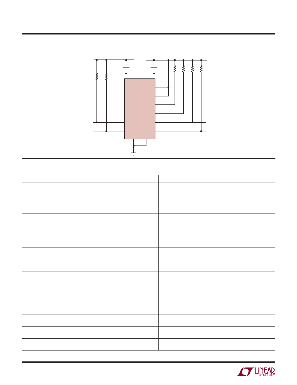
2.5V
R1
2.7k
R2
2.7k
C2
0.01μF
V
V
CC2
CC
DISCEN
3.3V
R3
10k
R4
10kR510k
R6
10k
LTC4309
SDAIN
SCLIN
GND
5V
C6
0.01MF
4309 F05
R13
2.7k
R14
2.7k
V
CC
SDA2
SCL2
14
ENABLE
READY
LTC4309
FAULT
SDA1
SCL1
SDAIN
SCLIN
GND
SDAOUT
SCLOUT
ACC
4309 F06
SDA2
SCL2
Figure 8. The LTC4309 in a level shifting application where the bus supplies are different from VCC.
4309fa

PACKAGE DESCRIPTION
LTC4309
DE/UE Package
12-Lead Plastic DFN (4mm x 3mm)
(Reference LTC DWG # 05-08-1695)
0.70 p0.05
3.60 p0.05
1.70 p0.05
(2 SIDES)
2.20 p0.05
0.25 p 0.05
3.30 p0.05
RECOMMENDED SOLDER PAD PITCH AND DIMENSIONS
PIN 1
TOP MARK
(NOTE 6)
0.200 REF
NOTE:
1. DRAWING PROPOSED TO BE A VARIATION OF VERSION
(WGED) IN JEDEC PACKAGE OUTLINE M0-229
2. DRAWING NOT TO SCALE
3. ALL DIMENSIONS ARE IN MILLIMETERS
(2 SIDES)
4.00 p0.10
(2 SIDES)
16-Lead Plastic SSOP (Narrow .150 Inch)
(Reference LTC DWG # 05-08-1641)
0.50
BSC
3.00 p0.10
0.75 p0.05
GN Package
PACKAGE OUTLINE
0.50
BSC
127
16
0.40 p 0.10
PIN 1 NOTCH
R = 0.20 OR
0.35 s 45o
CHAMFER
(UE12/DE12) DFN 0905 REV C
R = 0.115
TYP
R = 0.05
TYP
1.70 p 0.05
(2 SIDES)
(2 SIDES)
0.25 p 0.05
3.30 p0.05
0.00 – 0.05
4. DIMENSIONS OF EXPOSED PAD ON BOTTOM OF PACKAGE DO NOT INCLUDE MOLD
FLASH. MOLD FLASH, IF PRESENT, SHALL NOT EXCEED 0.15mm ON ANY SIDE
5. EXPOSED PAD SHALL BE SOLDER PLATED
6. SHADED AREA IS ONLY A REFERENCE FOR PIN 1 LOCATION
ON THE TOP AND BOTTOM OF PACKAGE
(2 SIDES)
BOTTOM VIEW—EXPOSED PAD
16
12
15
.189 – .196*
(4.801 – 4.978)
14
3
.254 MIN
RECOMMENDED SOLDER PAD LAYOUT
.007 – .0098
(0.178 – 0.249)
.016 – .050
(0.406 – 1.270)
NOTE:
1. CONTROLLING DIMENSION: INCHES
2. DIMENSIONS ARE IN
3. DRAWING NOT TO SCALE
(MILLIMETERS)
INCHES
.045 p.005
.150 – .165
.229 – .244
(5.817 – 6.198)
.0250 BSC.0165 p.0015
.015
p .004
(0.38 p 0.10)
0o – 8o TYP
* DIMENSION DOES NOT INCLUDE MOLD FLASH. MOLD FLASH
SHALL NOT EXCEED 0.006" (0.152mm) PER SIDE
** DIMENSION DOES NOT INCLUDE INTERLEAD FLASH. INTERLEAD
FLASH SHALL NOT EXCEED 0.010" (0.254mm) PER SIDE
s 45o
.0532 – .0688
(1.35 – 1.75)
.008 – .012
(0.203 – 0.305)
TYP
Information furnished by Linear Technology Corporation is believed to be accurate and reliable.
no responsibility is assumed for its use. Linear Technology Corporation makes no representation that
the interconnection of its circuits as described herein will not infringe on existing patent rights.
13
4
12 11 10
5
678
(0.635)
9
.004 – .0098
(0.102 – 0.249)
.0250
BSC
However,
.009
(0.229)
REF
.150 – .157**
(3.810 – 3.988)
GN16 (SSOP) 0204
4309fa
15
LTC4309
TYPICAL APPLICATION
R1
10k
R2
10k
5V to 3.3V Level Translator
C1
0.01MF
V
V
CC
CC2
DISCEN
ENABLE
READY
LTC4309
FAULT
C2
0.01MF
R3
10k
R4
10kR510k
R6
10k
5V3.3V
SDA1
SCL1
SDAIN
SCLIN
GND
SDAOUT
SCLOUT
ACC
4309 F07
SDA2
SCL2
RELATED PARTS
PART NUMBER DESCRIPTION COMMENTS
LTC1380/LTC1393 Single-Ended 8-Channel/Differential 4-Channel Analog
MUX with SMBus Interface
LTC1427-50 Micropower, 10-Bit Current Output DAC with SMBus
Interface
LTC1623 Dual High Side Switch Controller with SMBus Interface 8 Selectable Addresses/16 Channel Capability
LTC1663 SMBus Interface 10-Bit Rail to Rail Micropower DAC DNL < 0.75 LSB Max, 5-Lead SOT-23 Package
LTC1694/LTC1694-1 SMBus Accelerator Improved SMBus/I
2
LTC1695 SMBus/I
C Fan Speed Controller in ThinSOT™ 0.75Ω PMOS 180mA Regulator, 6-Bit DAC
LT1786F SMBus Controlled CCFL Switching Regulator 1.25A, 200kHz, Floating or Grounded Lamp Confi gurations
2
LTC1840 Dual I
LTC4300A-1/
C Fan Speed Controller Two 100μA 8-Bit DACs, Two Tach Inputs, Four GPIO
Hot Swappable 2-Wire Bus Buffers –1: Bus Buffer with READY, ACC and ENABLE
LTC4300A-2/
LTC4300A-3
LTC4301 Supply Independent Hot Swappable 2-Wire Bus Buffer Supply Independent
LTC4301L Hot Swappable 2-Wire Bus Buffer with Low Voltage Level
Translation
LTC4302-1/
Addressable 2-Wire Bus Buffer Address Expansion, GPIO, Software Controlled
LTC4302-2
LTC4303
LTC4304
LTC4305
LTC4306
Hot Swappable 2-Wire Bus Buffer with Stuck Bus
Recovery
2 or 4-Channel, 2 Wire Bus Multiplexers with Capacitance
Buffering
LTC4307 Low Offset Hot Swappable 2-Wire Bus Buffer with Stuck
Bus Recovery
LTC4307-1 High Defi nition Multimedia Interface (HDMI) Level Shifting
2-Wire Bus Buffer
ThinSOT is a trademark of Linear Technology Corporation
Linear Technology Corporation
16
1630 McCarthy Blvd., Milpitas, CA 95035-7417
(408) 432-1900 ● FAX: (408) 434-0507 ● www.linear.com
: 35Ω Single Ended/70Ω Differential, Expandable to 32
Low R
ON
Single or 16 Differential Channels
Precision 50uA+/–2.5% Tolerance Over Temperature, 4 Selectable
SMBus Addresses, DAC Powers up at Zero or Midscale
2
SMBus/I
2
C Devices
C Rise-Time, Ensures Data Integrity with Multiple
–2: Dual Supply Bus Buffer with READY and ACC
–3: Dual Supply Bus Buffer with READY and ENABLE
2
C Busses
and SCL
IN
Allows Bus Pull-Up Voltages as Low as 1V on SDA
Provides Automatic Clocking to Free Stuck I
2 or 4 Selectable Downstream Busses, Stuck Bus Disconnect, Rise
Time Accelerators, Fault Reporting, ± 10kV HBM ESD Tolerance
60mV Buffer Offset, 30ms Stuck Bus Disconnect and Recovery, Rise
Time Accelerators, ± 5kV HBM ESD Tolerance
60mV Buffer Offset, 3.3V to 5V Level Shifting,
± 5kV HBM ESD Tolerance
LT 0108 REV A • PRINTED IN USA
© LINEAR TECHNOLOGY CORPORATION 2006
IN
4309fa
 Loading...