

L DESIGN FEATURES
100k
20Ω
3.01k
1%
27.4k
1%
10µF
39k
1µF
BAS21
1.2k
38.3k
33pF
1.5nF
10µF
100V
0.1µF
t
ON
12k
PGDLYV
NEG
SYNC
R
CLASS
SHDN
V
CMP
R
CMP
ENDLY OSC SFST
LTC4269-1
GND
UVLO
V
PORTP
V
CC
T2P
T2P
FB
C
CMP
+
+
V
PORTN
383k
1%
3.01k
1%
10k
1nF
3.3nF
•
•
•
•
33mΩ
1%
FDS2582
10k
15Ω
150Ω
PE-68386
BAT54
100Ω
2200pF
MMBT3906 MMBT3904
1µF
1µF
16V
T1
PA2369NL
SENSE
–
SENSE
+
SG
PG
L1
0.18µH
22pF
100µF
5.1Ω
•
FDS8880
47µF
5V
5A
+
SMAJ58A
30.9Ω
24k
107k
10k
S1B
B1100 s 8 PLCS
2.2µF
100V
10µH
DO1608C-103
0.1µF
100V
36V
PDZ36B
BSS63LT1
V
PORTP
48V
AUXILIARY
POWER
–54V FROM
DATA PAIR
–54V FROM
SPARE PAIR
+
–
PD Controller ICs with Integrated
Flyback or Forward Controllers Meet
Demands of 25.5W PoE+
Introduction
The IEEE 802.3af Power over Ethernet (PoE) standard allows a powered
device (PD), such as an internet
protocol (IP) telephone, to draw up to
12.95W from an Ethernet cable. When
the 802.3af standard was drafted,
12.95W appeared sufficient to cover
the immediately imaginable range of
PD products (primarily IP phones).
Of course, application developers
are always far more innovative than
standards committees anticipate, so
new power-hungry applications for
PoE immediately started to appear,
such as dual-radio IEEE 802.11a/g
and 802.11n wireless access points,
security cameras with pan/tilt/zoom
motors, and color LCD IP video
phones. 12.95W was suddenly not
enough. The IEEE committee responded with the 802.3at standard,
which raises the available PD power
to 25.5W. The new “at” standard, commonly referred to as PoE+, also adds
a “handshaking” communications
requirement between PDs and power
sourcing equipment (PSEs), while allowing backward compatibility with
the legacy “af” standard.
New power control ICs are required
to take advantage of these expanded
requirements. The DC/DC conversion
and control schemes used for legacy
“af” PDs are not optimized for the increased power capability and feature
requirements of PoE+. For instance,
in both standards the 37V to 57V PoE
voltage is converted to lower voltages
that digital circuitry can tolerate.
This DC/DC conversion is handled
in the lower power 12.95W standard
with a conventionally rectified (i.e.,
diode rectified) flyback converter. The
higher power 25.5W standard is better
by Ryan Huff
served by a synchronously rectified
(i.e. MOSFET rectified) flyback or a
forward power supply topology.
To meet the new performance
requirements of PoE+, including
handshaking, Linear Technology offers
a new family of PD controller ICs that
integrate a front-end PD controller with
a high performance synchronously
rectified flyback (LTC4269-1) or a
forward (LTC4269-2) power supply
controller.
Features
Both parts combine a PD controller—which includes the handshaking
circuitry, Hot Swap™ FET, and input
protection—with a DC/DC power
supply controller. While the power
supply sections of the two parts are
very different, the PD controller in
both is identical.
6
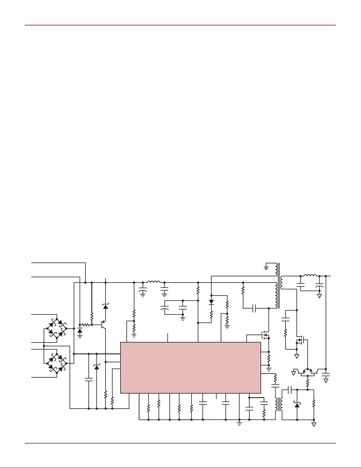
Figure 1. LTC4269-1-based synchronous flyback converter
Linear Technology Magazine • September 2009
+
T2P
T2P
V
NEG
V
PORTN
SHDN
SMAJ58A
R
CLASS
V
PORTP
PGND GND BLANK DELAY
82k
30.9Ω24k
158k 332k
133Ω
BAS516
BAS516
PA2431NL
BAS516
10k
IRF6217
FDS8880
FDS8880
5.1Ω
158k
22.1k
33k
1.5k
50mΩ
2k
5.1Ω
1.2k
TLV431A
PS2801-1-L
V
CC
11.3k
3.65k
22k
0.22µF
0.1µF
R
OSC
V
REF
FB
COMP
I
SENSE
OC
SS_MAXDC
FDS2582
SD_V
SEC
V
IN
S
OUT
LTC4269-2
0.1µF
18V
PDZ18B
10µF
16V
V
CC
33k
237k
107k
10.0k
S1B
B1100 s 8 PLCS
2.2µF
100V
+
10µF
100V
10µH
DO1608C-103
1mH
DO1608C-105
6.8µH
PG0702.682
10.0k
OUT
4.7nF
1nF
5.1Ω
1nF
0.1µF
100V
4.7nF
250V
10nF
+
220µF
6.3V
PSLVOJ227M(12)A
5V
5A
36V
PDZ36B
BSS63LT1
V
PORTP
–48V
AUXILIARY
POWER
–54V FROM
DATA PAIR
–54V FROM
BC857BF
•
•
•
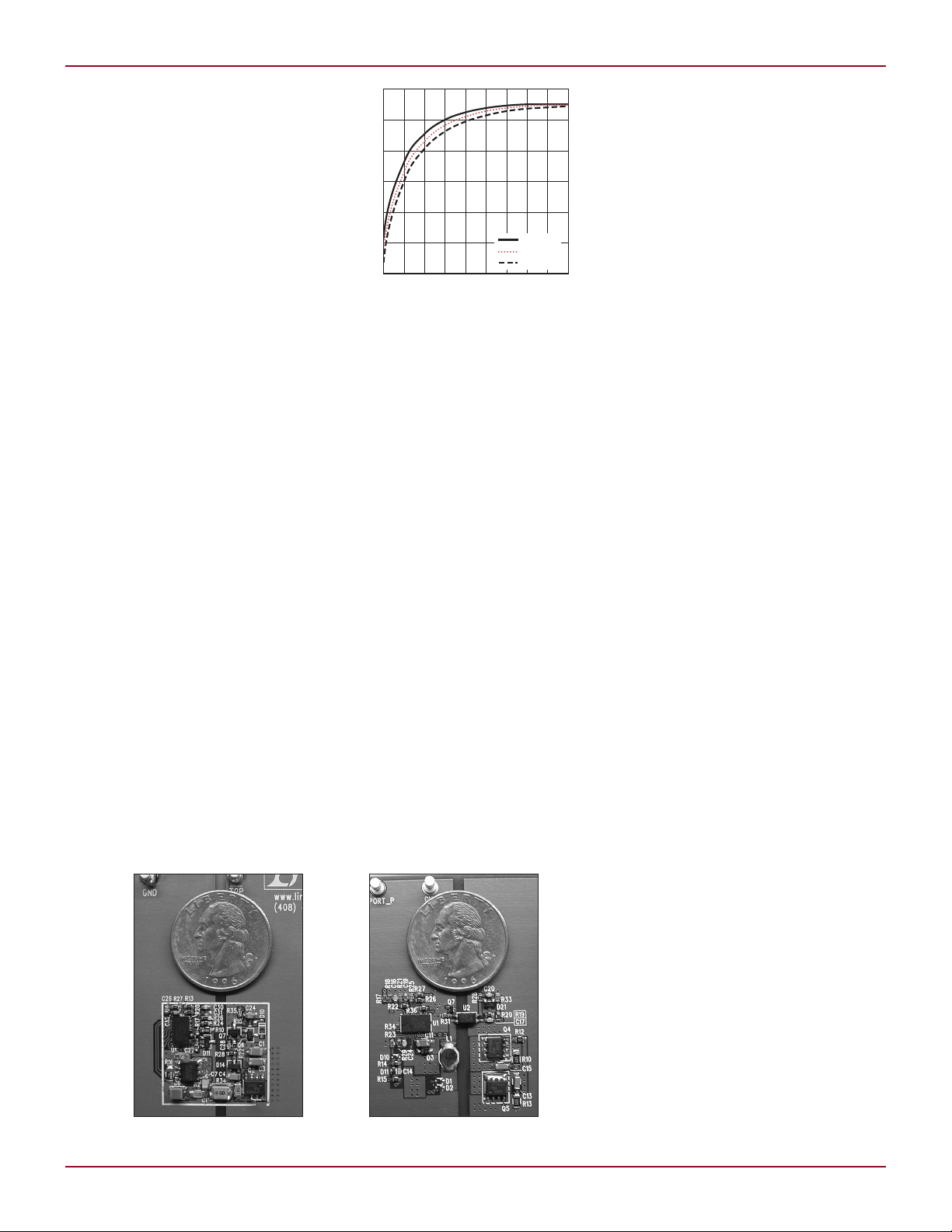
EFFICIENCY (%)
LOAD CURRENT (A)
50.5
95
65
1 1.5 2 2.5 3 3.5 4 4.5
70
75
85
80
90
VIN = 42V
VIN = 50V
VIN = 57V
In the LTC4269, handshaking circuitry, also known as the “High Power
Available,” “Two Finger Detect,” or
“Ping Pong” indicator, allows the PD
to take full advantage of a new PSE’s
full 25.5W of available power. Both
parts include an integrated Hot Swap
MOSFET for a controlled power up of
the PD. The switch has a low 700mΩ
(typical) resistance and a robust 100V
max rating, thus meeting the needs of
a wide range of applications. Auxiliary
power supplies (“wall warts”) can be
accommodated by interfacing to the
SHDN pin to disable the PoE power
path. Setting a programmable classification current allows different
power leveled PDs to be recognized
by the PSE. Achieving this is as easy
as choosing the proper resistor and
placing it from the R
pin. The ICs are chock-full of protection features, including overvoltage,
undervoltage, and overtemperature to
name a few. Finally, complementary
power good indicators signal that the
CLASS
pin to V
PORTN
PD Hot Swap MOSFET is out of the
inrush limit and ready to draw full
power.
The power supply controllers of the
LTC4269s also share some features.
Both offer programmable switching
frequency, which allows the designer
to optimize the trade-off between efficiency and size, or the designer can
choose a specific frequency to meet
application specific EMI requirements. The power supply soft-start
time is also adjustable to prevent
the PSE from dropping out its power
due to excessive inrush current and
virtually eliminate any power supply
DESIGN FEATURES L
Figure 3. LTC4269-2-based self-driven synchronous forward converter
Figure 2. Efficiency of the circuit in Figure 1
Linear Technology Magazine • September 2009
7
L DESIGN FEATURES
EFFICIENCY (%)
LOAD CURRENT (A)
50.5
95
65
1 1.5 2 2.5 3 3.5 4 4.5
70
75
85
80
90
VIN = 42V
VIN = 50V
VIN = 57V
output voltage overshoot. Both parts
include short circuit protection with
automatic restart.
LTC4269-1 Synchronous
Flyback for Optimized
Combination of Efficiency,
Simplicity, Size and Cost
A synchronous flyback supply utilizing the LTC4269-1 offers the best
combination of efficiency, simplicity,
size and cost. See Figures 1 and 2 for
the schematic and efficiency curves,
respectively, for an LTC4269-1-based
PD power supply capable of a 5V output voltage at 5A.
The flyback parts count is low for a
few reasons. There is no need for the
large output inductor that a forward
converter (see Figure 3) needs, for this
function is rolled into the isolation
transformer (T1). A small, inexpensive
second-stage filter inductor (L1) is
used in the flyback in order to reduce
output voltage ripple, but it should not
be confused with a traditional output
inductor.
In the case of the LTC4269-1, nei
ther a secondary side reference nor an
optocoupler are needed to transmit the
output voltage regulation information
across the isolation boundary. This is
because the IC uses the third (bias)
winding on the transformer, T1, to get
the output voltage information across
the boundary. Finally, the synchronous flyback topology requires half
of the switching MOSFETs (only two)
needed by the forward converter.
Performance, in terms of efficiency, tops out at above 90% for the
-
Figure 4. Efficiency of the circuit in Figure 3
LTC4269-1 synchronous flyback. As
a contrast, typical PoE efficiencies at
the “af” power level for a conventionally rectified flyback were in the lower
half of the 80%’s. This higher efficiency is due to the IC’s well-controlled
implementation of the synchronous
rectifier’s gate drive. This efficiency
is not attainable with an uncontrolled
self-driven synchronous rectification
scheme that is sometimes used.
Regulation over the full PoE+ input
voltage range and 0A to 5A output current range for the LTC4269-1 is better
than ±1%. Output voltage ripple for
the fundamental switching frequency
is less than 30mV peak-to-peak.
LTC4269-2
Synchronous Forward
to Maximize Efficiency
If the efficiency of a PoE+ power supply
is paramount, an LTC4269-2-based
synchronous forward supply is the answer at 92.5% efficiency. The increased
efficiency comes with the trade-off of
increased circuit size and complexity.
Figure 3 shows a complete PD power
supply. Figure 4 shows efficiency,
and Figure 5 compares the physical
size of the flyback (LTC4269-1) versus
the forward (LTC4269-2). The forward
supplies 5V at 5A.
The increase in the forward’s efficiency comes about in part from
decreased RMS currents in the secondary side MOSFETs and in part from
separating the transformer and output
inductor. Both of these changes from
the flyback reduce resistive losses.
The forward supply uses twice the
number of MOSFETs as a flyback so
each switch handles just a portion
of the current that the switches in
the flyback do, thus reducing the I2R
power losses. By separating the isolation transformer and output inductor,
instead of using the transformer for
both as in the flyback, the same power
is processed through two components
instead of one. The net effect is more
copper, thus less resistance and lower
resistive losses.
The cost of the circuit obviously
increases with the addition of larger
and more expensive power path
components. Complexity also goes
up with the need to control twice as
many MOSFETs. Also, the forward
topology does not lend itself to the
third winding feedback method. This
means extra complexity in the design
and compensation of a secondary side
reference and opto-coupler circuitry.
Other than the ultra high efficiency
of the LTC4269-2’s synchronous
forward, the solution has similar performance to the flyback. The output
ripple of the fundamental switching
frequency is about 40mV peak-topeak. The regulation over the entire
input voltage and load current range
is well under ±1%.
8
Figure 5. LTC4269-1 and -2 solutions
Conclusion
Two new highly integrated PD controller ICs are fully compliant with, and
take full advantage of, the upcoming
IEEE 802.3at PoE+ standard. The
LTC4269 family of parts support the
preferred high performance power
supply topologies for use in the new
standard.
Linear Technology Magazine • September 2009
L
 Loading...