

LTC4263
Single IEEE 802.3af
Compliant PSE Controller
with Internal Switch
FEATURES
n
IEEE 802®.3af Compliant
n
Operation from a Single 48V Supply
n
Fully Autonomous Operation without
Microcontroller
n
Internal MOSFET with Thermal Protection
n
Power Management Works Across Multiple Ports
with Simple RC Network
n
Precision Inrush Control with Internal Sense Resistor
n
Powered Device (PD) Detection and Classifi cation
n
AC and DC Disconnect Sensing
n
Robust Short-Circuit Protection
n
Pin-Selectable Detection Backoff for Midspan PSEs
n
Classifi cation Dependent I
n
LED Driver Indicates Port On and Blinks
Current Threshold
CUT
Status Codes
n
Available in 14-Pin SO and 4mm × 3mm DFN
Packages
APPLICATIONS
n
IEEE 802.3af Compliant Endpoint/Midspan PSEs
n
Single-Port or Multi-Port Power Injectors
n
Power Forwarders
n
Low-Port Count PSEs
n
Environment B PSEs
n
Standalone PSEs
L, LT, LTC and LTM are registered trademarks of Linear Technology Corporation.
All other trademarks are the property of their respective owners.
DESCRIPTION
The LTC®4263 is an autonomous single-channel PSE
controller for use in IEEE 802.3af compliant Power over
Ethernet systems. It includes an onboard power MOSFET,
internal inrush, current limit, and short-circuit control,
IEEE 802.3af compliant PD detection and classifi cation
circuitry, and selectable AC or DC disconnect sensing.
Onboard control algorithms provide complete IEEE 802.3af
compliant operation without the need of a microcontroller.
The LTC4263 simplifi es PSE implementation, needing
only a single 48V supply and a small number of passive
support components.
Programmable onboard power management circuitry
permits multiple LTC4263s to allocate and share power
in multi-port systems, allowing maximum utilization of
the 48V power supply—all without the intervention of a
host processor. The port current limit can be confi gured
to automatically adjust to the detected PD class. Detection backoff timing is confi gurable for either Endpoint or
Midspan operation. Built-in foldback and thermal protection
provide comprehensive fault protection.
An LED pin indicates the state of the port controlled by
the LTC4263. When run from a single 48V supply, the LED
pin can operate as a simple switching current source to
reduce power dissipation in the LED drive circuitry.
The LTC4263 is available in 14-pin 4mm × 3mm DFN and
14-pin SO packages.
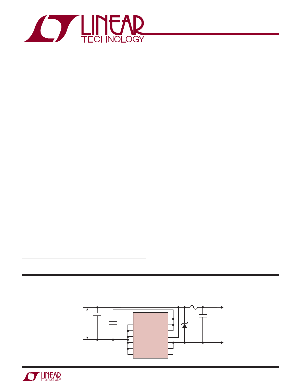
TYPICAL APPLICATION
+
ISOLATED
48V SUPPLY
–
Single-Port Fully Autonomous PSE
0.1μF
100V
0.1μF
LED
LEGACY
MIDSPAN
PWRMGT
V
SS
V
SS
OSC
LTC4263
V
DD5
ENFCLS
SD
V
DD48
OUT
OUT
ACOUT
1A
SMAJ58A
0.1μF
100V
TO PORT
MAGNETICS
4263 TA01
4263fd
1
LTC4263
ABSOLUTE MAXIMUM RATINGS
Supply Voltages
V
SS
V
DD5
– V
........................................ V
........................................... 0.3V to –80V
DD48
– 0.3V to V
SS
SS
+ 6V
Pin Voltages and Currents
LEGACY, MIDSPAN, ENFCLS, PWRMGT
SD, OSC .................................. V
LED ....................................... V
– 0.3V to V
SS
– 0.3V to V
SS
SS
SS
+ 6V
+ 80V
OUT, ACOUT ............................................ (See Note 3)
PIN CONFIGURATION
TOP VIEW
LED
1
LEGACY
MIDSPAN
PWRMGT
EXPOSED PAD (PIN 15) IS V
2
3
4
V
5
SS
6
V
SS
7
OSC
14-LEAD (4mm s 3mm) PLASTIC DFN
T
JMAX
DE14 PACKAGE
= 125°C, θJA = 43°C/W, θJC = 4.3°C/W
15
, MUST BE SOLDERED TO PCB
SS
14
13
12
11
10
9
8
V
DD5
ENFCLS
SD
V
DD48
OUT
OUT
ACOUT
(Notes 1, 2)
Operating Ambient Temperature Range
LTC4263C ................................................ 0°C to 70°C
LTC4263I ............................................. –40°C to 85°C
Junction Temperature (Note 4) ............................. 125°C
Storage Temperature Range ................... –65°C to 150°C
Lead Temperature (Soldering, 10 sec)
SO ..................................................................... 300°C
TOP VIEW
1
LED
2
LEGACY
MIDSPAN
PWRMGT
3
4
5
V
SS
6
V
SS
7
OSC
S PACKAGE
14-LEAD PLASTIC SO
T
= 125°C, θJA = 90°C/W, θJC = 37°C/W
JMAX
14
13
12
11
10
9
8
V
DD5
ENFCLS
SD
V
DD48
OUT
OUT
ACOUT
ORDER INFORMATION
LEAD FREE FINISH TAPE AND REEL PART MARKING* PACKAGE DESCRIPTION TEMPERATURE RANGE
LTC4263CDE#PBF LTC4263CDE#TRPBF 4263
LTC4263IDE#PBF LTC4263IDE#TRPBF 4263
14-Lead (4mm × 3mm) Plastic DFN
14-Lead (4mm × 3mm) Plastic DFN
LTC4263CS#PBF LTC4263CS#TRPBF 4263CS 14-Lead Plastic SO 0°C to 70°C
LTC4263IS#PBF LTC4263IS#TRPBF 4263IS 14-Lead Plastic SO –40°C to 85°C
Consult LTC Marketing for parts specifi ed with wider operating temperature ranges. *The temperature grade is identifi ed by a label on the shipping container.
For more information on lead free part marking, go to: http://www.linear.com/leadfree/
For more information on tape and reel specifi
ELECTRICAL CHARACTERISTICS
The
temperature range, otherwise specifi cations are at TA = 25°C. V
cations, go to: http://www.linear.com/tapeandreel/
l denotes the specifi cations which apply over the full operating
– VSS = 48V and V
DD48
not driven externally. All voltages are
DD5
relative to VSS unless otherwise noted. (Notes 2, 5)
SYMBOL PARAMETER CONDITIONS MIN TYP MAX UNITS
Power Supplies
V
SUPPLY
V
UVLO_OFF
V
UVLO_HYS
48V Supply Voltage V
UVLO Turn-Off Voltage V
UVLO Hysteresis
– V
DD48
SS
To Maintain IEEE Compliant Output
– VSS Decreasing
DD48
l
33
l
46
l
29 31 33 V
l
0.1 1 V
0°C to 70°C
–40°C to 85°C
48 66
57
4263fd
V
V
2

LTC4263
ELECTRICAL CHARACTERISTICS
The l denotes the specifi cations which apply over the full operating
temperature range, otherwise specifi cations are at T
relative to VSS unless otherwise noted. (Notes 2, 5)
SYMBOL PARAMETER CONDITIONS MIN TYP MAX UNITS
V
OVLO_OFF
V
OVLO_HYS
V
DD5
I
DD48
I
DD5
Power MOSFET
R
ON
I
OUT_LEAK
R
PU
Current Control
I
CUT
I
LIM
I
FB
I
MIN
I
FAULT
Detection
I
DET
V
DET
R
DETMIN
R
DETMAX
R
OPEN
Classifi cation
V
CLASS
I
CLASS
I
TCLASS
Power Management
V
PWRMGT
I
PWRMGT
AC Disconnect
R
OSC
I
OSC
f
OSC
OVLO Turn-Off Voltage V
OVLO Hysteresis
V
Supply Voltage Driven Externally
DD5
V
Internal Supply Driven Internally
DD5
V
Supply Current V
DD48
V
Supply Current V
DD5
On-Resistance I = 350mA, Measured From OUT to V
OUT Pin Leakage V
OUT Pin Pull-Up Resistance to V
DD48
Overload Current Threshold Class 0, Class 3, Class 4 (Note 6)
Short-Circuit Current Limit V
Foldback Current Limit V
DC Disconnect Current Threshold
High Speed Fault Current Limit (Note 8)
Detection Current First Point, V
Detection Voltage Compliance V
Minimum Valid Signature Resistance
Maximum Valid Signature Resistance
Open Circuit Threshold
Classifi cation Voltage V
Classifi cation Current Compliance V
Classifi cation Threshold Current Class 0 – 1
Power Management Pin Threshold
Power Management Pin Output Current Class 0, Class 3, Class 4
OSC Pin Input Impedance 2V ≤ (V
OSC Pin Output Current V
OSC Pin Frequency V
= 25°C. V
A
DD48
– VSS Increasing
DD48
– VSS = 5V
DD5
Internal V
– VSS = 5V
DD5
– VSS = V
OUT
0V ≤ (V
Class 2
Class 1
– VSS = 5V
OUT
V
– V
DD48
– V
DD48
V
– V
DD48
Second Point, V
– V
DD48
V
– VSS = 57V
DD48
– V
DD48
= V
OUT
Class 1 – 2
Class 2 – 3 (Note 9)
Class 1
Class 2
– VSS = 2V
OSC
– VSS = 2V
OSC
– VSS = 48V and V
DD5
– VSS = 57V
DD48
– V
DD48
OUT
OUT
OUT
OUT
OUT
DD48
OSC
) ≤ 5V
OUT
= 30V
= 0V (Note 7)
= 10V
– V
DD48
– V
DD48
, Open Port
, 0mA ≤ I
– VSS) ≤ 3V
OUT
OUT
CLASS
= 10V
= 3.5V
≤ 50mA
not driven externally. All voltages are
DD5
l
66 70 74 V
l
0.2 2 V
l
4.5 5 5.5 V
l
4.3 4.4 4.5 V
SS
l
l
l
l
l
l
360 500 640
l
355
l
165
l
95
l
405
l
405
l
30
l
110
l
5.2 7.5 9.8 mA
l
500 650 800 mA
l
235
l
160
l
l
15.5 17 18.5
l
27.5 29.7 32
l
500 2000
l
16.5 20.5 V
l
55 60 75 mA
l
5.5
l
13.5
l
21.5
l
0.98 1 1.02 V
l
–75.6
l
–19.6
l
–34.3
l
175 250 325
l
–140 140 μA
l
103 110 115 Hz
1
2
12mA
1.5 2.4
110 μA
375
175
100
425
425
60
140
255
180
6.5
14.5
23
–72.3
–18.8
–32.8
–17.9
–31.3
2
4
3.0
395
185
105
445
445
120
180
275
200
21 V
7.5
15.5
24.5
–69
4263fd
mA
mA
kΩ
mA
mA
mA
mA
mA
mA
mA
μA
μA
kΩ
kΩ
kΩ
mA
mA
mA
μA
μA
μA
kΩ
Ω
Ω
3

LTC4263
ELECTRICAL CHARACTERISTICS
The l denotes the specifi cations which apply over the full operating
temperature range, otherwise specifi cations are at T
= 25°C. V
A
relative to VSS unless otherwise noted. (Notes 2, 5)
SYMBOL PARAMETER CONDITIONS MIN TYP MAX UNITS
A
VACD
I
ACDMAX
I
ACDMIN
V
ACDEN
Digital Interface (Note 10)
V
OLED
V
ILD
V
IHD
V
OZ
I
OLEG
I
FLT
Timing Characteristics
t
DET
t
DETDLY
t
PDC
t
PON
t
RISE
t
OVLD
t
ED
t
MPDO
t
MPS
t
DBO
t
DISDLY
Note 1: Stresses beyond those listed under Absolute Maximum Ratings
may cause permanent damage to the device. Exposure to any Absolute
Maximum Rating condition for extended periods may affect device
reliability and lifetime.
Note 2: All currents into device pins are positive; all currents out of device
pins are negative. All voltages are referenced to V
specifi ed.
Note 3: 80mA of current may be pulled from the OUT or ACOUT pin
without damage whether the LTC4263 is powered or not. These pins will
also withstand a positive voltage of V
Note 4: This IC includes overtemperature protection that is intended
to protect the device during momentary overload conditions. Junction
temperature will exceed 125°C when overtemperature protection is active.
Continuous operation above the specifi ed maximum operating junction
temperature may impair device reliability.
Note 5: The LTC4263 operates with a negative supply voltage. To avoid
confusion, voltages in this data sheet are referred to in terms of absolute
magnitude.
Voltage Gain OSC to ACOUT 2V ≤ (V
AC Disconnect Output Current V
Remain Connected AC Pin Current V
AC Disconnect Enable Signal V
LED Output Low Voltage I
OSC
OSC
OSC
LED
Digital Input Low Voltage MIDSPAN, PWRMGT, ENFCLS, SD LEGACY
Digital Input High Voltage MIDSPAN, PWRMGT, ENFCLS, SD LEGACY
Voltage of Legacy Pin if Left Floating
Current In/Out of Legacy Pin 0V ≤ (V
Maximum Allowed Leakage of External Components
at Legacy Pin in Force Power-On Mode
Detection Time Beginning to End of Detection
Detection Delay PD Insertion to Detection Complete
Classifi cation Duration
Power Turn-On Delay End of Valid Detect to Application of Power
Turn-On Rise Time V
DD48
C
PSE
Overload/Short-Circuit Time Limit
Error Delay I
CUT
Maintain Power Signature (MPS) Disconnect Delay PD Removal to Power Removal
MPS Minimum Pulse Width PD Minimum Current Pulse Width
Required to Stay Connected (Note 11)
Midspan Mode Detection Backoff
R
PORT
Power Removal Detection Delay
unless otherwise
SS
+ 80V.
SS
– VSS = 48V and V
DD48
– VSS) ≤ 3V
OSC
– V
= 2V, 0V ≤ (V
SS
– VSS = 2V
– VSS, Port On
= 10mA
– VSS) ≤ 5V
LEGACY
– V
: 10% to 90%
OUT
= 0.1μF
Fault to Next Detect
= 15.5kΩ
Note 6: If the ENFCLS pin is high, I
classifi cation. If ENFCLS pin is low, I
Note 7: In order to reduce power dissipated in the switch while charging
the PD, the LTC4263 reduces the current limit when V
Refer to the Typical Performance Characteristics for more information.
Note 8: The LTC4263 includes a high speed current limit circuit intended to
protect against faults. The fault protection is activated for port current
in excess of I
circuit current limit (I
levels.
Note 9: Class 4 or higher classifi cation current is treated as Class 3.
Note 10: The LTC4263 digital interface operates with respect to V
logic levels are measured with respect to V
Note 11: The IEEE 802.3af specifi cation allows a PD to present its
Maintain Power Signature (MPS) on an intermittent basis without being
disconnected. In order to stay powered, the PD must present the MPS for
within any t
t
MPS
not driven externally. All voltages are
DD5
l
0.95 1.0 1.05 V/V
– VSS) ≤ 4V
ACOUT
. After the high speed current limit activates, the short-
FAULT
LIM
time window.
MPDO
l
–1 1 mA
l
130 160 190 μA
l
1.5 V
l
l
l
l
2.2
l
2.2
l
1.1 1.25 1.4 V
l
–60 60 μA
l
–10 10 μA
l
270 290 310 ms
l
300 620 ms
l
34 37 39 ms
l
135 145 155 ms
l
40 170 μs
l
52 62 72 ms
l
3.8 4.0 4.2 s
l
320 350 380 ms
l
l
3.0 3.2 3.4 s
l
0.8 0.95 1.1 s
depends on the result of
CUT
reverts to its Class 0 specifi cation.
CUT
1.1 2.2 V
– VSS is large.
OUT
) engages and restricts current to IEEE 802.3af
.
SS
0.8
0.4
20 ms
. All
SS
V
V
V
4
4263fd
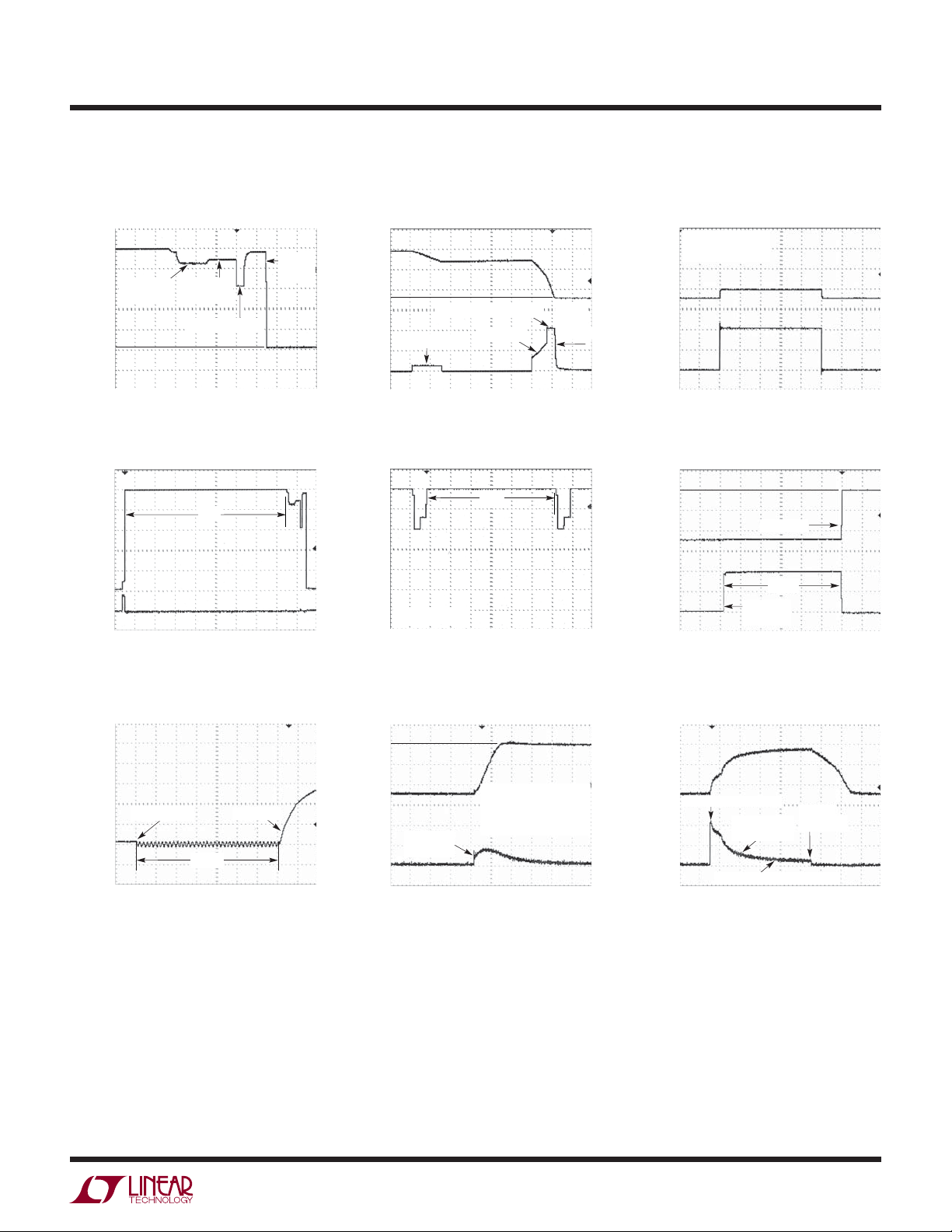
TYPICAL PERFORMANCE CHARACTERISTICS
LTC4263
Powering an IEEE 802.3af PD
V
DD48
V
OUT
10V/DIV
V
DETECTION
PHASE 1
SS
DETECTION
PHASE 2
CLASSIFICATION
100ms/DIV
Overload Restart Delay
V
DD48
t
ED
V
OUT
10V/DIV
V
SS
I
PORT
500mA/
DIV
500ms/DIV
POWER
ON
4263 G01
4263 G10
V
DD48
V
OUT
20V/DIV
V
400mA
I
OUT
200mA/DIV
0mA
V
DD48
V
OUT
2V/DIV
Powering a Legacy PD with
220μF Bypass Capacitor
SS
425mA CURRENT LIMIT
CLASSIFICATION
FOLDBACK
25ms/DIV
LOAD
FULLY
CHARGED
4263 G02
V
DD48
V
DD48
20mA/DIV
Classifi cation Transient
Response to 40mA Load Step
V
– VSS = 48V
DD48
T
= 25°C
A
V
OUT
2V/DIV
– 18V
– 19V
40mA
I
OUT
0mA
100μs/DIV
Midspan Backoff with Invalid PD Overcurrent Response Time
V
DD48
V
OUT
20V/DIV
V
400mA
I
OUT
200mA/DIV
0mA
SS
PORT OFF
LOAD
APPLIED
10ms/DIV
t
OVLD
R
PORT
= 15.5kΩ
t
DBO
500ms/DIV
4263 G11
4263 G06
4263 G12
Response to PD Removal with
AC Disconnect Enabled Rapid Response to 1Ω Short
V
DD48
V
OUT
10V/DIV
V
SS
PD REMOVAL
t
MPDO
50ms/DIV
PORT OFF
4263 G13
I
PORT
20A/
DIV
V
DD48
V
OUT
20V/DIV
V
20A
SS
1Ω SHORT
APPLIED
0A
I
= CURRENT IN
PORT
1Ω RESISTOR APPLIED
TO OUTPUT OF CIRCUIT
ON FRONT PAGE
1μs/DIV
4263 G14
V
DD48
V
OUT
20V/DIV
V
800mA
I
PORT
400mA/DIV
0mA
Rapid Response to
Momentary 50Ω Short
SS
50Ω SHORT APPLIED
CURRENT
LIMIT ACTIVE
FOLDBACK CURRENT LIMIT
= CURRENT IN 50Ω RESISTOR APPLIED
I
PORT
TO OUTPUT OF CIRCUIT ON FRONT PAGE
SHORT
REMOVED
100μs/DIV
4263 G15
4263fd
5
LTC4263
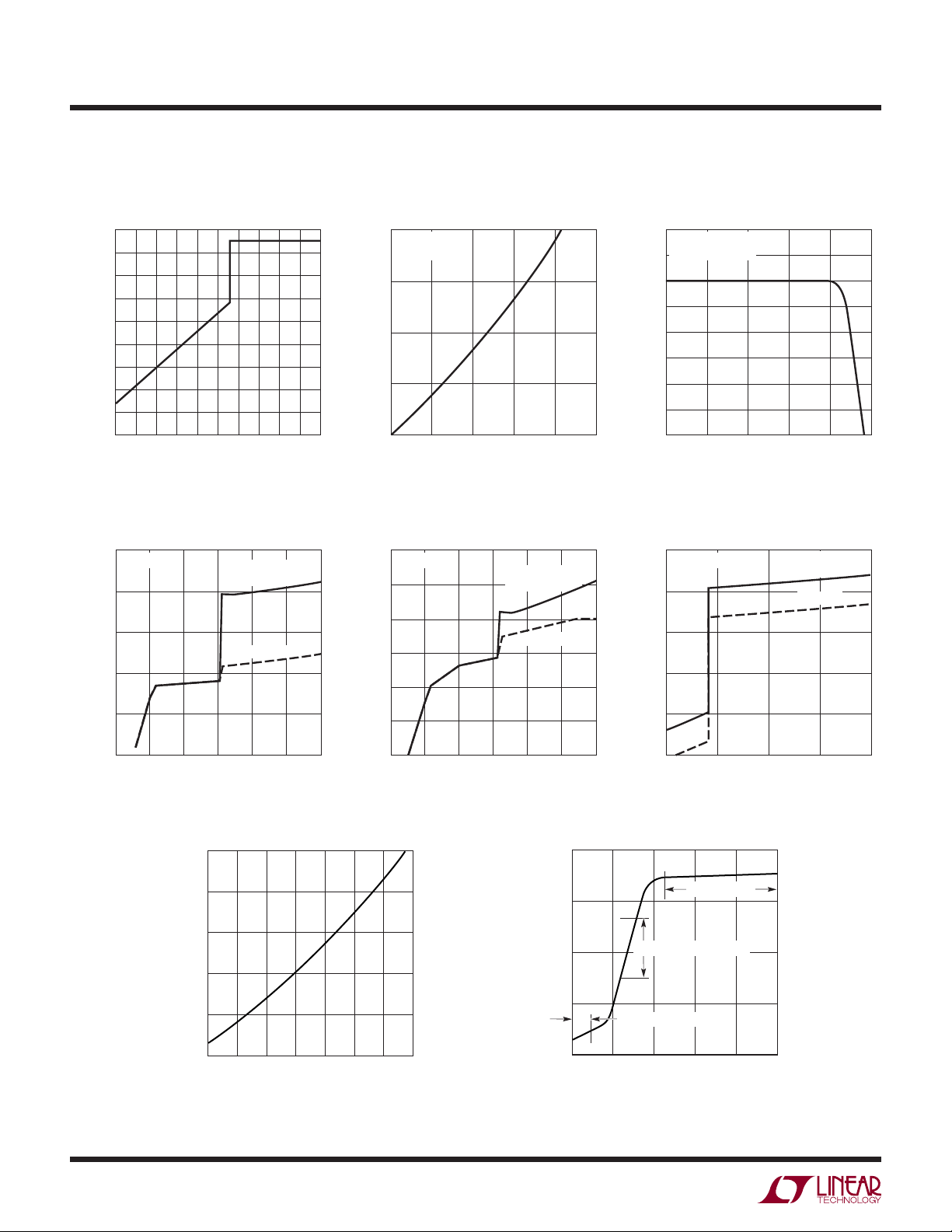
TYPICAL PERFORMANCE CHARACTERISTICS
LED Pin Pulldown
Current Limit and Foldback
450
400
350
300
250
(mA)
200
OUT
I
150
100
50
0
5 10152025 50
0
I
DD48
V
– V
DD48
DC Supply Current vs Supply
Voltage with Internal V
2.5
TA = 25°C
2.0
1.5
(mA)
DD48
1.0
I
30 35 40 45
OUT
4263 G03
DD5
25k LOAD WITH
AC ENABLED
NO LOAD
vs Load Current Classifi cation Current Compliance
4
TA = 25°C
INTERNAL V
3
2
PIN PULLDOWN (V)
LED
1
V
0
0
I
DD48
Supply Voltage with V
1.2
TA = 25°C
1.0
0.8
(mA)
0.6
DD48
I
0.4
DD5
10 20 30 40 50
I
LOAD CURRENT (mA)
LED
DC Supply Current vs
= 5.0V
DD5
25k LOAD WITH
AC ENABLED
NO LOAD
4263 G04
80
V
– VSS = 48V
DD48
T
= 25°C
A
70
60
50
(mA)
40
OUT
I
30
20
10
0
04
I
DC Supply Current
DD5
vs Supply Voltage
2
V
= 48V
DD48
1
0
(mA)
DD5
I
–1
8121620
V
– V
DD48
(V)
OUT
25k LOAD WITH
AC ENABLED
NO LOAD
4263 G05
0.5
0
10 20 30 40 50 60
0
V
DD48
(V)
RON vs Temperature Legacy Pin Current vs Voltage
2.0
1.8
1.6
(Ω)
ON
R
1.4
1.2
1.0
–40 –20
4263 G07
40
20
0
TEMPERATURE (°C)
0.2
0
10 20 30 40 50 60
0
80
100
4263 G16
60
V
DD48
(V)
40
20
(μA)
LEGACY
I
–20
–40
4263 G08
0
0
–2
–3
4.0
FORCE POWER ON MODE
COMPLIANT MODE
1
2
V
LEGACY
4.5 5.0 5.5 6.0
V
DD5
LEGACY MODE
3
4
5
(V)
4263 G17
4263 G09
4263fd
6
TEST TIMING
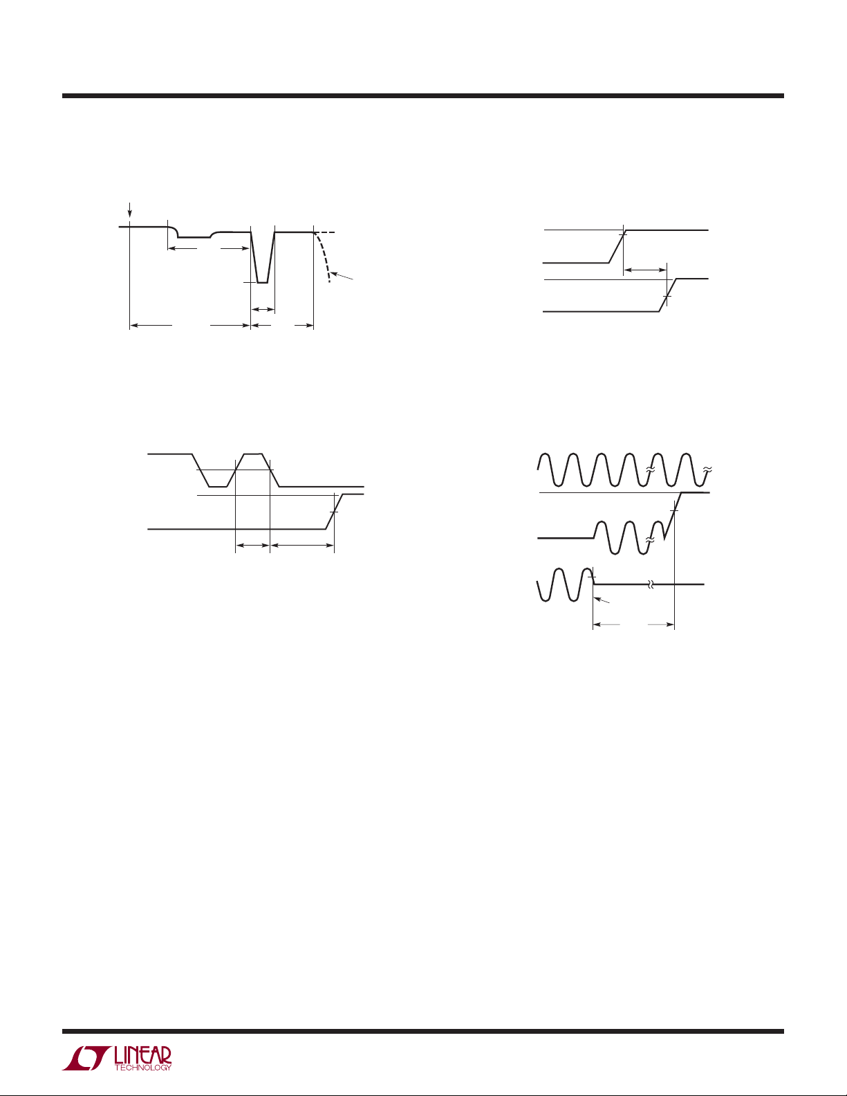
Detect, Class and Turn-On Timing Current Limit Timing
PD
INSERTED
V
DD48
V
OUT
t
DETDLY
DC Disconnect Timing AC Disconnect Timing
t
DET
V
CLASS
t
PON
t
PDC
4263 TT01
PORT
TURN-ON
LTC4263
I
LIM
I
OUT
V
DD48
V
OUT
V
SS
I
CUT
t
OVLD
4263 TT02
I
V
V
OUT
OUT
SS
V
I
MIN
DD48
t
MPS
t
MPDO
V
OSC
V
OUT
I
ACOUT
V
DD48
V
SS
I
ACDMIN
PD REMOVED
t
MPDO
4263 TT04
4263fd
7

LTC4263
PIN FUNCTIONS
(DFN/SO)
LED (Pin 1): Port State LED Drive. This pin is an open drain
output that pulls down when the port is powered. Under port
fault conditions, the LED will fl ash in patterns to indicate
the nature of the port fault. See the Applications Information section for a description of these patterns. When the
LTC4263 is operated from a single 48V supply, this pin is
pulsed low with a 6% duty cycle during the periods when
the LED should be on. This allows use of a simple inductor,
diode, and resistor circuit to avoid excess heating due to
the large voltage drop from V
. See the Applications
DD48
Information section for details on this circuit.
LEGACY (Pin 2): Legacy Detect. This pin controls whether
legacy detect is enabled. If held at V
, legacy detect is
DD5
enabled and testing for a large capacitor is performed to
detect the presence of a legacy PD on the port. See the
Applications Information section for descriptions of legacy
PDs that can be detected. If held at V
, only IEEE 802.3af
SS
compliant PDs are detected. If left fl oating, the LTC4263
enters force-power-on mode and any PD that generates
between 1V and 10V when biased with 270μA of detection
current will be powered as a legacy device. This mode is
useful if the system uses a differential detection scheme
to detect legacy devices. Warning: Legacy modes are not
IEEE 802.3af compliant.
MIDSPAN (Pin 3): Midspan Enable. If this pin is connected
to V
, Midspan backoff is enabled and a 3.2 second
DD5
delay occurs after every failed detect cycle unless the
result is open circuit. If held at V
, no delay occurs after
SS
failed detect cycles.
PWRMGT (Pin 4): Power Management. The LTC4263
sources current at the PWRMGT pin proportional to the
class of the PD that it is powering. The voltage of this pin
is checked before powering the port. The port will not
turn on if this pin is more than 1V above V
. Connect the
SS
PWRMGT pins of multiple LTC4263s together with a resistor
and capacitor to V
power management is not used, tie this pin to V
(Pins 5, 6): Negative 48V Supply. Pins 5 and 6 should
V
SS
to implement power management. If
SS
.
SS
be tied together on the PCB.
OSC (Pin 7) Oscillator for AC Disconnect. If AC disconnect is used, connect a 0.1μF X7R capacitor from OSC to
. Tie OSC to VSS to disable AC disconnect and enable
V
SS
DC disconnect.
ACOUT (Pin 8): AC Disconnect Sense. Senses the port
to determine whether a PD is still connected when in AC
disconnect mode. If port capacitance drops below about
0.15μF for longer than T
the port is turned off. If
MPDO
AC disconnect is used, connect this pin to the port with
a series combination of a 1k resistor and a 0.47μF 100V
X7R capacitor. See the Applications Information section
for more information.
OUT (Pins 9, 10): Port Output. If DC disconnect is used,
these pins are connected to the port. If AC disconnect is
used, these pins are connected to the port through a parallel
combination of a 1A diode and a 500k resistor. Pins 9 and
10 should be tied together on the PCB. See the Applications
Information section for more information.
(Pin 11): 48V Return. Must be bypassed with a
V
DD48
0.1μF capacitor to V
SS
.
SD (Pin 12): Shutdown. If held low, the LTC4263 is pre-
vented from performing detection or powering the port.
Pulling SD low will turn off the port if it is powered. When
released, a 4-second delay will occur before detection is
attempted.
ENFCLS (Pin 13): Enforce Class Current Limits. If held
at V
, the LTC4263 will reduce the I
DD5
class 1 or class 2 PDs. If ENFCLS is held at V
threshold for
CUT
SS
, I
CUT
remains at 375mA (typ) for all classes.
(Pin 14): Logic Power Supply. Apply 5V referenced
V
DD5
, if such a supply is available, or place a 0.1μF
to V
SS
bypass capacitor to V
to enable the internal regulator.
SS
When the internal regulator is used, this pin should only
be connected to the bypass capacitor and to any logic pins
of the LTC4263 that are being held at V
Exposed Pad (Pin 15, DE Package Only): V
connected to V
on the PCB. The Exposed Pad acts as a
SS
DD5
.
. Must be
SS
heatsink for the internal MOSFET.
8
4263fd

BLOCK DIAGRAM
14
R
LED
+
48V
–
TO OTHER LTC4263s
+
5V
–
R
PM
C
PM
0.1μF
1
4
5
6
7
V
DD5
LED
PWRMGT
V
SS
OSC
V
DD5
CONTROL
HOT SWAP
INT5 EXT5
LTC4263
1A
V
DD48
11
SD
12
ENFCLS
500k
13
2
3
9
10
8
LEGACY
MIDSPAN
SMAJ58A
500k
OUT
0.47μF
1k
ACOUT
5V REG
4
I
DET
0.1μF
TO PORT
MAGNETICS
BOLD LINES INDICATE HIGH CURRENT
4263 BD
4263fd
9

LTC4263
APPLICATIONS INFORMATION
POE OVERVIEW
Over the years, twisted-pair Ethernet has become the most
commonly used method for local area networking. The
IEEE 802.3 group, the originator of the Ethernet standard,
has defi ned an extension to the standard, IEEE 802.3af,
which allows DC power to be delivered simultaneously
over the same cable used for data communication. This
has enabled a whole new class of Ethernet devices, including IP telephones, wireless access points, and PDA
charging stations which do not require additional AC
wiring or external power transformers, a.k.a. “wall warts.”
With about 13W of power available, small data devices
can be powered by their Ethernet connections, free from
AC wall outlets. Sophisticated detection and power monitoring techniques prevent damage to legacy data-only
devices while still supplying power to newer, Ethernetpowered devices over the twisted-pair cable.
The device that supplies power is called the Power Sourcing Equipment (PSE). A device that draws power from the
wire is called a Powered Device (PD). A PSE is typically an
Ethernet switch, router, hub, or other network switching
equipment that is commonly found in the wiring closets
where cables converge. PDs can take many forms. Digital
IP telephones, wireless network access points, PDA or
notebook computer docking stations, cell phone chargers,
and HVAC thermostats are examples of devices that can
draw power from the network.
A PSE is required to provide a nominal 48V DC between
either the signal pairs or the spare pairs (but not both)
as shown in Figure 1. The power is applied as a voltage
between two of the pairs, typically by powering the center taps of the isolation transformers used to couple the
differential data signals to the wire. Since Ethernet data
is transformer coupled at both ends and is sent differentially, a voltage difference between the transmit pairs and
the receive pairs does not affect the data. A 10Base-T/
100Base-TX Ethernet connection only uses two of the four
pairs in the cable. The unused or spare pairs can optionally be powered directly, as shown in Figure 1, without
affecting the data. 1000Base-T uses all four pairs and
power must be connected to the transformer center taps
if compatibility with 1000Base-T is required.
The LTC4263 provides a complete PSE solution for detection and powering of PD devices in an IEEE 802.3af
compliant system. The LTC4263 controls a single PSE
port that will detect, classify, and provide isolated 48V
power to a PD device connected to the port. The LTC4263
senses removal of a PD with IEEE 802.3af compliant AC
or DC methods and turns off 48V power when the PD is
disconnected. An internal control circuit takes care of
system confi guration and timing.
–48V RETURN
–48V SUPPLY
10
0.1μF
0.1μF
CAT 5
PSE PD
0.1μF
V
DD48
LTC4263
V
DD5
V
SS
OUT
Tx
Rx
SMAJ58A
58V
RJ45
4
5
1
2
3
6
7
6
20Ω MAX
ROUNDTRIP
0.05μF MAX
SPARE PAIR
DATA PAIR
DATA PAIR
SPARE PAIR
RJ45
4
5
1
Rx
2
3
Tx
6
7
6
Figure 1. System Diagram
1N4002
s4
1N4002
s4
0.1μF
SMAJ58A
58V
R
CLASS
–48V
GND
–48V
LTC4267-BASED
PD/SWITCHER
IN
OUT
OUT
5mF ≤ C
≤ 300μF
IN
+
V
OUT
–
4263 F01
4263fd

APPLICATIONS INFORMATION
LTC4263
LTC4263 OPERATION
Signature Detection
The IEEE 802.3af specifi cation defi nes a specifi c pair-topair signature resistance used to identify a device that
can accept power via its Ethernet connection. When the
port voltage is below 10V, an IEEE 802.3af compliant
PD will have an input resistance of approximately 25kΩ.
Figure 2 illustrates the relationship between the PD signature resistance and the required resistance ranges the
PSE must accept and reject. According to the IEEE 802.3af
specifi cation, the PSE must accept PDs with signatures
between 19kΩ and 26.5kΩ and may or may not accept
resistances in the two ranges of 15kΩ to 19kΩ and 26.5kΩ
to 33kΩ. The black box in Figure 2 represents the typical
150Ω pair-to-pair termination used in Ethernet devices
like a computer’s network interface card (NIC) that cannot
accept power.
RESISTANCE
0Ω 10k
150Ω (NIC)
PD
PSE
REJECT ACCEPT REJECT
20k 30k
15k
19k
26.25k23.75k
26.5k
33k
Figure 2. IEEE 802.3af Signature Resistance Ranges
4263 F02
60
PSE LOAD
50
40
30
CURRENT (mA)
20
10
0
0
OVER
CURRENT
CLASS 4
CLASS 3
LINE
V
DD48
CLASS 2
CLASS 1
CLASS 0
– V
TYPICAL
CLASS 3
PD LOAD
5101520
OUT
LINE
48mA
33mA
23mA
14.5mA
6.5mA
25
4263 F04
Figure 3. PD 2-Point Detection
the line to settle and measuring the resulting voltage. This
result is stored and the second current is applied to the
port, allowed to settle and the voltage measured.
The LTC4263 will not power the port if the PD has more
than 5μF in parallel with its signature resistor unless legacy
mode is enabled.
The LTC4263 autonomously tests for a valid PD connected
to the port. It repeatedly queries the port every 580ms, or
every 3.2s if midspan backoff mode is active (see below).
If detection is successful, it performs classifi cation and
power management and then powers up the port.
The LTC4263 checks for the signature resistance by forcing
two test currents on the port in sequence and measuring
the resulting voltages. It then subtracts the two V-I points
to determine the resistive slope while removing voltage
offset caused by any series diodes or current offset caused
by leakage at the port (see Figure 3). The LTC4263 will
typically accept any PD resistance between 17kΩ and
29.7kΩ as a valid PD. Values outside this range (excluding open and short-circuits) are reported to the user by a
code fl ashed via the LED pin.
The LTC4263 uses a force-current detection method in
order to reduce noise sensitivity and provide a more robust
detection algorithm. The fi rst test point is taken by forcing
a test current into the port, waiting a short time to allow
Midspan Backoff
IEEE 802.3af requires the midspan PSE to wait two seconds
after a failed detection before attempting to detect again
unless the port resistance is greater than 500kΩ. This
requirement is to prevent the condition of an endpoint PSE
and a midspan PSE, connected to the same PD at the same
time, from each corrupting the PD signature and preventing power-on. After the fi rst corrupted detection cycle, the
midspan PSE waits while the endpoint PSE completes
detection and turns the port on. If the midspan mode of
the LTC4263 is enabled by connecting the MIDSPAN pin
to V
, a 3.2 second delay occurs after every failed detect
DD5
cycle unless the result is an open circuit.
4263fd
11

LTC4263
APPLICATIONS INFORMATION
Classifi cation
An IEEE 802.3af PD has the option of presenting a classifi cation signature to the PSE to indicate how much power
it will draw when operating. This signature consists of a
specifi c constant-current draw when the PSE port voltage is between 15.5V and 20.5V, with the current level
60
PSE LOAD
OVER
TYPICAL
CLASS 3
PD LOAD
LINE
V
DD48
CURRENT
CLASS 4
CLASS 3
CLASS 2
CLASS 1
CLASS 0
– V
50
40
30
CURRENT (mA)
20
10
0
0
5101520
Figure 4. Classifi cation Load Lines
OUT
LINE
48mA
33mA
23mA
14.5mA
6.5mA
25
4263 F04
indicating the power class to which the PD belongs. Per
the IEEE 802.3af specifi cation, there are fi ve classes and
three power levels for a PD as shown in Table 1. Note that
class 4 is presently reserved by the IEEE for future use.
Figure 4 shows an example PD load line, starting with the
shallow slope of the 25k signature resistor below 10V, then
drawing the classifi cation current (in this case, class 3)
between 15.5V and 20.5V. Also shown is the load line for
the LTC4263. It maintains a low impedance until reaching
current limit at 60mA (typ).
The LTC4263 will classify a port immediately after a
successful detection. It measures the PD classifi cation
signature current by applying 18V (typ) to the port and
measuring the resulting current. The LTC4263 identifi es
the three IEEE power levels and stores the detected class
internally for use by the power management circuitry. In
addition, the LTC4263 allows selectable enforcement of
IEEE classifi cation power levels. With the ENFCLS pin
high, the LTC4263 reduces the I
current threshold if it
CUT
detects class 1 or class 2, thereby insuring that PDs which
violate their advertised class are shut down.
Table 1. IEEE 802.3af Classifi cation, PD Power Consumption, and LTC4263 Enforced Power Output
IEEE 802.3af
CLASS
0 0mA to 5mA 12.95W 375mA (typ) PD Does Not Implement Classifi cation, Unknown Power
1 8mA to 13mA 3.84W 100mA (typ) Low Power PD
2 16mA to 21mA 6.49W 175mA (typ) Medium Power PD
3 25mA to 31mA 12.95W 375mA (typ) Full Power PD
4 35mA to 45mA 12.95W 375mA (typ) Reserved, Power as Class 0
*Enforced I
CLASSIFICATION
CURRENT
active if ENFCLS pin is high. Otherwise, I
CUT
MAXIMUM
IEEE ALLOWABLE
PD POWER
is 375mA (typ).
CUT
LTC4263
ENFORCED I
THRESHOLD* CLASS DESCRIPTION
CUT
12
4263fd

APPLICATIONS INFORMATION
LTC4263
Power Management
The LTC4263 includes a power management feature
allowing simple implementation of power management
across multiple ports driven by a single power supply. The
PWRMGT pins of all LTC4263 devices are tied together
along with an RC network to prevent over-allocation of
power in a multi-port system.
Immediately following classifi cation, the LTC4263 performs
a power management check to ensure power is available
to supply the newly classed PD. The allocated power is
represented by the voltage on the shared PWRMGT node
and the LTC4263 checks the allocated power by measuring this voltage. If the PWRMGT voltage is less than 1V,
there is power available and the power needs of the new
PD are added to the already allocated power on the node.
To allocate power, a current proportional to the power
needs for the new PD is sourced out of the PWRMGT pin
(Table 2).
Table 2. LTC4263 Power Management
IEEE 802.3af
CLASS
0, 3, 4 15.4W –72.3μA
2 7W –32.8μA
1 4W –18.8μA
PSE OUTPUT
POWER REQUIRED
LTC4263 PWRMGT
CURRENT
When additional current is added to the PWRMGT node,
the voltage rises toward the 1V threshold. After adding
current, the LTC4263 verifi es that the power supply is not
over-allocated by verifying the node voltage remains below
1V. If the voltage is below 1V, the LTC4263 proceeds to
power the port. If over 1V, the current is removed from
the node, port powering is aborted, and the LTC4263 goes
back into detection mode.
For multiple LTC4263s implementing power management,
the PWRMGT pins are connected together and to a RC
network connected to V
represents the full load output capability of the system
R
PM
power supply (P
FULL_LOAD
as shown in Figure 5. The value of
SS
). Select a 1% resistor to set the
full load output power using the following formula:
kW
PM
213 Ω •
=
P
FULL LOAD
_
R
The LTC4263 power management uses pulse width
modulation to set the power requirements of each PD.
Capacitor C
is used as a lowpass fi lter to generate the
PM
average power requirement for all PDs in the system. Set
to 1μF.
C
PM
If power management is not used, tie PWRMGT to V
PWRMGT
LTC4263
V
SS
PWRMGT
LTC4263
V
SS
PWRMGT
LTC4263
V
SS
R
PM
V
SS
Figure 5. PWRMGT Pin Connections
C
1μF
PM
PWRMGT
LTC4263
V
SS
4263 F05
SS
.
4263fd
13

LTC4263
APPLICATIONS INFORMATION
Power Control
The primary function of the LTC4263 is to control the
delivery of power to the PSE port. In order to meet IEEE
802.3af requirements and provide a robust solution, a
variety of current limit and current monitoring functions
are needed, as shown in Figure 6. All control circuitry
is integrated and the LTC4263 requires no external
MOSFET, sense resistor, or microcontroller to achieve
IEEE compliance.
The LTC4263 includes an internal MOSFET for driving
the PSE port. The LTC4263 drives the gate of the internal
MOSFET while monitoring the current and the output voltage at the OUT pin. This circuitry couples the 48V input
supply to the port in a controlled manner that satisfi es
the PD’s power needs while minimizing disturbances on
the 48V backplane.
500mA
CURRENT LIMIT
400mA
PORT OFF IN t
OVLD
I
INRUSH
refers to current at port turn-on and I
is the maxi-
LIM
mum allowable current in the case of a short after the port is
powered. Because the IEEE specifi cation calls out identical
values, the LTC4263 implements both as a single current
limit referred to as I
LIM
.
When 48V power is applied to the port, the LTC4263 is
designed to power-up the PD in a controlled manner without
causing transients on the input supply. To accomplish this,
the LTC4263 implements inrush current limit. At turn-on,
current limit will allow the port voltage to quickly rise
until the PD reaches its input turn-on threshold. At this
point, the PD begins to draw current to charge its bypass
capacitance, slowing the rate of port voltage increase.
If at any time the port is shorted or an excessive load is
applied, the LTC4263 limits port current to avoid a hazardous condition. The current is limited to I
for port
LIM
voltages above 30V and is reduced for lower port voltages
(see the Foldback section). Inrush and short-circuit current limit are allowed to be active for 62ms (typ) before
the port is shut off.
300mA
LIMIT
(I
LIM
NORMAL
OPERATION
)
DC DISCONNECT
PORT OFF IN t
MPDO
4263 F07
PORT CURRENT
200mA
100mA
0mA
DC DISCONNECT
(I
MIN
Figure 6. Current Thresholds and Current Limits
CUT
)
(I
)
CUT
Port Overload
A PSE port is permitted to supply up to 15.4W continuously
and up to 400mA (I
) for up to 75ms (t
CUT
OVLD
) when in
overload. Per the IEEE 802.3af specifi cation, the PSE is
required to remove power if a port stays in an overload
condition. The LTC4263 monitors port current and removes
port power if port current exceeds 375mA (typ) for greater
than 62ms (typ).
Port Inrush and Short-Circuit
The IEEE 802.3af standard lists two separate maximum
current limits, I
INRUSH
and I
, that a PSE must implement.
LIM
Port Fault
If the port is suddenly shorted, the internal MOSFET power
dissipation can rise to very high levels until the short-circuit
current limit circuit can respond. A separate high speed
(I
current limit circuit detects severe fault conditions
650mA (typ)
) and quickly turns off the internal MOSFET if
such an event occurs. The circuit then limits current to I
while the t
will be reduced by the foldback circuitry.
I
LIM
Timing
t
OVLD
timer increments. During a short-circuit,
OVLD
OUT
>
LIM
For overload, inrush, and short-circuit conditions, the
IEEE 802.3af standard limits the duration of these events
to 50ms-75ms. The LTC4263 includes a 62ms (typ) t
OVLD
timer to monitor overload conditions. The timer is incremented whenever current greater than I
the port. If the current is still above I
fl ows through
CUT
when the t
CUT
OVLD
timer expires, the LTC4263 will turn off power to the port
and fl ash the LED. In this situation, the LTC4263 waits
four seconds and then restarts detection. If the overload
14
4263fd

APPLICATIONS INFORMATION
LTC4263
condition is removed before the t
timer expires, the
OVLD
port stays powered and the timer is reset.
Foldback
Foldback is designed to limit power dissipation in the
LTC4263 during power-up and momentary short-circuit
conditions. At low port output voltages, the voltage
across the internal MOSFET is high, and power dissipation will be large if signifi cant current is fl owing. Foldback
monitors the port output voltage and reduces the I
LIM
current limit level for port voltages of less than 28V, as
shown in Figure 7.
500
400
300
(mA)
LIM
I
200
100
0
51015
0
V
DD48
Figure 7. Current Limit Foldback
20 25
– V
30 35 45
40
(V)
OUT
50
4263 F07
Thermal Protection
The LTC4263 includes thermal overload protection in
order to provide full device functionality in a miniature
package while maintaining safe operating temperatures.
Several factors create the possibility for very large power
dissipation within the LTC4263. At port turn-on, while
is active, the instantaneous power dissipated by the
I
LIM
LTC4263 can be as high as 12W. This can cause 40ºC or
more of die heating in a single turn-on sequence. Similarly,
excessive heating can occur if an attached PD repeatedly
pushes the LTC4263 into I
rent. Excessive heating can also occur if the V
by drawing too much cur-
LIM
DD5
pin is
shorted or overloaded.
The LTC4263 protects itself from thermal damage by
monitoring die temperature. If the die temperature exceeds
the overtemperature trip point, the LTC4263 removes port
power and shuts down all functions including the internal
5V regulator. Once the die cools, the LTC4263 waits four
seconds, then restarts detection.
DC Disconnect
The DC disconnect circuit monitors port current whenever
power is on to detect continued presence of the PD. IEEE
802.3af mandates a minimum current of 10mA that the
PD must draw for periods of at least 75ms with optional
dropouts of no more than 250ms. The t
disconnect
MPDO
timer increments whenever port current is below 7.5mA
(typ). If the timer expires, the port is turned off and the
LTC4263 waits 1.5 seconds before restarting detection.
If the undercurrent condition goes away before t
MPDO
(350ms (typ)), the timer is reset to zero. The DC discon-
nect circuit includes a glitch fi lter to prevent noise from
falsely resetting the timer. The current must be present for
a period of at least 20ms to guarantee reset of the timer.
To enable DC disconnect, tie the OSC pin to V
AC Disconnect
AC disconnect is an alternate method of sensing the presence or absence of a PD by monitoring the port impedance.
The LTC4263 forces an AC signal from an internal sine wave
generator on to the port. The ACOUT pin current is then
sampled once per cycle and compared to I
ACDMIN
disconnect, the AC disconnect sensing circuitry controls the
disconnect timer. When the connection impedance
t
MPDO
rises due to the removal of the PD, AC peak current falls
below I
ACDMIN
and the disconnect timer increments. If the
impedance remains high (AC peak current remains below
I
ACDMIN
), the disconnect timer counts to t
port is turned off. If the impedance falls, causing AC peak
current to rise above I
ACDMIN
for two consecutive samples
before the maximum count of the disconnect timer, the
timer resets and the port remains powered.
The AC disconnect circuitry senses the port via the ACOUT
pin. Connect a 0.47μF 100V X7R capacitor (C
a 1kΩ resistor (R
) from the DETECT pin to the port
DET
output as shown in Figure 8. This provides an AC path for
sensing the port impedance. The 1kΩ resistor, R
current fl owing through this path during port power-on and
power-off. An AC blocking diode (D
) is inserted between
AC
the OUT pin and the port to prevent the AC signal from
SS
MPDO
.
. Like DC
and the
) and
DET
, limits
DET
4263fd
15

LTC4263
APPLICATIONS INFORMATION
+
ISOLATED
48V SUPPLY
–
0.1μF
100V
NC
0.1μF
0.1μF
Figure 8. LTC4263 Using AC Disconnect
LTC4263
LED
LEGACY
MIDSPAN
PWRMGT
V
SS
V
SS
OSC ACOUT
V
DD5
ENFCLS
SD
V
DD48
OUT
OUT
500k
D
AC
CMLSH05-4
R
DET
1k
1A
SMAJ58A
C
DET
0.47μF
X7R, 100V
C
PSE
0.1μF
X7R, 100V
4263 F08
being shorted by the LTC4263’s power control MOSFET.
The 500k resistor across D
allows the port voltage to
AC
decay after disconnect occurs.
Sizing of capacitors is critical to ensure proper function
of AC disconnect. C
(Figure 8) controls the connection
PSE
impedance on the PSE side. Its capacitance must be kept
low enough for AC disconnect to be able to sense the PD.
On the other hand, C
has to be large enough to pass
DET
the signal at 110Hz. The recommended values are 0.1μF
for C
and R
and 0.47μF for C
PSE
are chosen to create an economical, physically
DET
. The sizes of C
DET
PSE
, C
DET
,
compact and functionally robust system. Moreover, the
complete Power over Ethernet AC disconnect system (PSE,
transformers, cabling, PD, etc.) is complex; deviating from
the recommended values of C
DET
, R
DET
and C
is strongly
PSE
discouraged. Contact the Linear Technology Applications
department for additional support.
Internal 110Hz AC Oscillator
The LTC4263 includes onboard circuitry to generate a
110Hz (typ), 2V
sine wave on its OSC pin when a
P-P
0.1μF capacitor is connected between the OSC pin and
V
. This sine wave is synchronized to the controller
SS
inside the LTC4263 and should not be externally driven.
Tying the OSC pin to V
shuts down the oscillator and
SS
enables DC disconnect.
Power-On Reset and Reset/Backoff Timing
Upon start-up, the LTC4263 waits four seconds before
starting its fi rst detection cycle. Depending on the results of this detection it will either power the port, repeat
detection, or wait 3.2 seconds before attempting detection
again if in midspan mode.
The LTC4263 may be reset by pulling the SD pin low. The
port is turned off immediately and the LTC4263 sits idle.
After SD is released there will be a 4-second delay before
the next detection cycle begins.
Logic-Level Supply
V
DD5
The V
externally or generated internally from the V
supply for the LTC4263 can either be supplied
DD5
supply.
DD48
If supplied externally, a voltage between 4.5V and 5.5V
should be applied to the V
regulator to shut down. If V
pin to cause the internal
DD5
is to be generated inter-
DD5
nally, the voltage will be 4.4V (typ) and a 0.1μF capacitor
should be connected between V
connect the internally generated V
and VSS. Do not
DD5
to anything other
DD5
than a bypass capacitor and the logic control pins of the
same LTC4263.
LED Flash Codes
The LTC4263 includes a multi-function LED driver to inform
the user of the port status. The LED is turned on when the
port is connected to a PD and power is applied. If the port
is not connected or is connected to a non-powered device
with a 150Ω or shorted termination, the port will not be
powered and the LED will be off. For other port conditions,
the LTC4263 blinks a code to communicate the status
to the user as shown in Table 3. One fl ash indicates low
signature resistance, two fl ashes indicates high resistance,
fi ve fl ashes indicates an overload fault, and nine fl ashes
indicates that power management is preventing the port
from turning on.
4263fd
16

APPLICATIONS INFORMATION
LTC4263
When active, the LED fl ash codes are repeated every 1.2
seconds. The duration of each LED fl ash is 75ms. Multiple
LED fl ashes occur at a 300ms interval.
The LTC4263 includes a feature for effi ciently driving the
LED from a 48V power supply without the wasted power
caused by having to drop over 45V in a current limit
resistor. When operating the V
supply internally, the
DD5
LTC4263 drives the LED pin with a 6% duty cycle PWM
signal. This allows use of the simple LED drive circuit in
Figure 9 to minimize power dissipation. The modulation
frequency of the LED drive is 28kHz, making the on period
V
DD48
D1
10mH, 21mA
COILCRAFT
DS1608C-106
R
LED
1k
V
SS
0.1μF
Figure 9. LED Drive Circuit with Single 48V Supply
LED
V
DD5
D2
BAS19
V
LTC4263
DD48
4263 F09
2.2μs. During the 2.2μs that the LED pin is pulled low, current ramps up in the inductor, limited by R
. Diode D2
LED
completes the circuit by allowing current to circulate while
the LED pin is open circuit. Since current is only drawn
from the power supply 6% of the time, power dissipation
is substantially reduced.
When V
is powered from an external supply, the PWM
DD5
signal is disabled and the LED pin will pull down continuously when on. In this mode, the LED can be powered from
the 5V supply with a simple series resistor.
IEEE 802.3af COMPLIANCE AND EXTERNAL
COMPONENT SELECTION
This section discusses the other elements that go along
with the LTC4263 to make an IEEE 802.3af compliant PSE.
The LTC4263 is designed to control power delivery in IEEE
802.3af compliant Power Sourcing Equipment. Because
proper operation of the LTC4263 also depends on external
components and power sources like the 48V supply, using
the LTC4263 in a PSE does not in itself guarantee IEEE
802.3af compliance. To ensure a compliant PSE design,
it is recommended to adhere closely to the example application circuits provided. For further assistance contact
the Linear Technology Applications department.
Table 3. Port Status and LED Flash Codes
PORT STATUS LED FLASH CODE FLASH PATTERN
Non-Powered Device
0Ω < R
Port Open
R
PORT
Port On
25kΩ
Low Signature Resistance
300Ω < R
High Signature Resistance
33kΩ < R
Port Overload Fault 5 Flashes
Power Management
Allocation Exceeded
PORT
> 1MΩ
PORT
PORT
< 200Ω
< 15kΩ
< 500kΩ
Off LED Off
Off LED Off
On LED On
1 Flash
2 Flashes
9 Flashes
4263fd
17

LTC4263
APPLICATIONS INFORMATION
Common Mode Chokes
Both non-powered and powered Ethernet connections
achieve best performance for data transfer and EMI when a
common mode choke is used on each port. For cost reduction reasons, some designs share a common mode choke
between two adjacent ports. This is not recommended.
Sharing a common mode choke between two ports couples
start-up, disconnect and fault transients from one port
to the other. The end result can range from momentary
noncompliance with IEEE 802.3af to intermittent behavior
and even to excessive voltages that may damage circuitry
in both the PSE and PD connected to the port.
Transient Suppressor Diode
IEEE 802.3af Power over Ethernet is a challenging Hot
Swap™ application because it must survive unintentional
abuse by repeated plugging in and out of devices at the
port. Ethernet cables could potentially be cut or shorted
together. Consequently, the PSE must be designed to
handle these events without damage.
The most severe of these events is a sudden short on a
powered port. What the PSE sees depends on how much
CAT-5 cable is between it and the short. If the short occurs on the far end of a long cable, the cable inductance
will prevent the current in the cable from increasing too
quickly and the LTC4263 built-in short-circuit protection
will control the current and turn off the port. However,
the high current along with the cable inductance causes
a large fl yback voltage to appear across the port when the
MOSFET is turned off. In the case of a short occurring
with a minimum length cable, the instantaneous current
can be extremely high due to the lower inductance. The
LTC4263 has a high speed fault current limit circuit that
shuts down the port in 20μs (typ). In this case, there is
lower inductance but higher current so the event is still
severe. A transient suppressor is required to clamp the port
voltage and prevent damage to the LTC4263. An SMAJ58A
or equivalent device works well to maintain port voltages
within a safe range. A bidirectional transient suppressor
should not be used. Good board layout places the transient
suppressor between the port and the LTC4263 to enhance
the protective function.
If the port voltage reverses polarity and goes positive, the
OUT pin can be overstressed because this voltage is stacked
on top of the 48V supply. In this case, the transient suppressor must clamp the voltage to a small positive value
to protect the LTC4263 and the PSE capacitor.
Component leakages across the port can have an adverse
affect on AC disconnect and even affect DC disconnect if
the leakage becomes severe. The SMAJ58A is rated at less
than 5μA leakage at 58V and works well in this application. There is a potential for stress induced leakage, so
suffi cient margins should be used when selecting transient
suppressors for these applications.
Hot Swap is a trademark of Linear Technology Corporation.
18
4263fd

APPLICATIONS INFORMATION
LTC4263
Capacitors
Sizing of both the C
DET
and C
capacitors is critical for
PSE
proper operation of the LTC4263 AC disconnect sensing.
See the AC Disconnect section for more information. Note
that many ceramic capacitors have dramatic DC voltage
and temperature coeffi cients. Use 100V or higher rated
X7R capacitors for C
DET
and C
, as these have reduced
PSE
voltage dependence while also being relatively small and
inexpensive. Bypass the 48V supply with a 0.1μF, 100V
capacitor located close to the LTC4263. The V
DD5
supply
also requires a 0.1μF bypass capacitor.
Fuse
While the LTC4263 does not require a fuse for proper
operation or for compliance with IEEE 802.3af, some
safety requirements state that the output current must be
limited to less than 2A in less than 60 seconds if any one
component fails or is shorted. Since the LTC4263 is the
primary current limiter, its failure could result in excess
current to the port. To meet these safety requirements, a
fuse can be placed in the positive leg of the port. The fuse
must be large enough that it will pass at least 450mA when
derated for high temperature but small enough that it will
fuse at less than 2A at cold temperature. This requirement
can usually be satisfi ed with a 1A fuse or PTC. Placing the
fuse between the RJ-45 connector and the LTC4263 and
its associated circuitry provides additional protection for
this circuitry. Consult a safety requirements expert for the
application specifi c requirements.
Power Supply
Poor regulation on the 48V supply can lead to noncompliance. The IEEE specifi cation requires a PSE output voltage
between 44V and 57V. When the LTC4263 begins powering
an Ethernet port, it controls the current through the port to
minimize disturbances on V
. However, if the VSS supply
SS
is underdamped or otherwise unstable, its voltage could
go outside of the IEEE-specifi ed limits, causing the PSE
to be noncompliant. This scenario can be even worse
when a PD is unplugged because the current can drop
immediately to zero. In both cases the port voltage must
always stay between 44V and 57V. Beyond this, the IEEE
802.3af specifi cation places specifi c ripple, noise and load
regulation requirements on the PSE. Disturbances on V
SS
can also adversely affect detection, classifi cation and AC
disconnect sensing. For these reasons, proper bypassing
and stability of the V
Another problem that can affect the V
supply is important.
SS
SS
supply is insuffi cient power, leading to the supply voltage dropping out
of the specifi ed range. The 802.3af specifi cation states
that if a PSE powers a PD it must be able to provide the
maximum power level requested by the PD based on the
PD’s classifi cation. The specifi cation does allow a PSE
to choose not to power a port, typically because the PD
requires more power than the PSE has available to deliver.
If a PSE is built with a V
supply not capable of deliver-
SS
ing full power to all ports, it is recommended to use the
LTC4263 power management feature to prevent ports
from being turned on when there is insuffi cient power.
Because the specifi cation also requires the PSE to supply an inrush current of 400mA at up to a 5% duty cycle,
the V
supply capability should be at least a few percent
SS
higher than the maximum total power the PSE needs to
supply to the PDs.
4263fd
19

LTC4263
APPLICATIONS INFORMATION
Isolation
The IEEE 802.3af standard requires Ethernet ports to be
electrically isolated from all other conductors that are user
accessible. This includes the metal chassis, other connectors, and the AC power line. Environment A isolation is
the most common and applies to wiring within a single
building serviced by a single AC power system. For this
type of application, the PSE isolation requirement can be
met with the use of a single, isolated 48V supply powering
several LTC4263 ports. Environment B, the stricter isolation requirement, is for networks that cross an AC power
distribution boundary. In this case, electrical isolation
must be maintained between each port in the PSE. The
LTC4263 can be used to build a multi-port Environment B
PSE by powering each LTC4263 from a separate, isolated
48V supply. In all PSE applications, there should be no
user accessible connections to the LTC4263 other than
the RJ-45 port.
20
4263fd

TYPICAL APPLICATIONS
Three Port Midspan PSE with Power Management Set for 30W
LTC4263
ISOLATED
48V
0.1μF
0.1μF
14
12
2
3
13
5
6
14
12
2
3
13
5
6
LTC4263
V
DD5
SD
LEGACY
MIDSPAN
ENFCLS
V
SS
V
SS
LTC4263
V
DD5
SD
LEGACY
MIDSPAN
ENFCLS
V
SS
V
SS
V
DD48
LED
PWRMGT
OSC
ACOUT
OUT
OUT
V
DD48
LED
PWRMGT
OSC
ACOUT
OUT
OUT
MIDSPAN
IN
1
0.1μF
100V
11
1
4
7
8
10
9
11
1
4
7
8
10
9
1k
0.1
100V
0.1μF
100V
1k
0.1μF
100V
2
3
4
5
6
7
8
RJ45 RJ45
μF
SMAJ58A
MIDSPAN
IN
1
2
3
4
5
6
7
8
RJ45 RJ45
SMAJ58A
MIDSPAN
OUT
1
2
3
4
5
6
7
8
MIDSPAN
OUT
1
2
3
4
5
6
7
8
0.1μF
14
12
2
3
13
5
6
LTC4263
V
DD5
SD
LEGACY
MIDSPAN
ENFCLS
V
SS
V
SS
V
DD48
LED
PWRMGT
OSC
ACOUT
OUT
OUT
MIDSPAN
IN
1
0.1μF
100V
11
1
4
7
8
10
9
1k
0.1μF
100V
R
PM
7.15k
1%
2
3
4
5
6
7
8
RJ45 RJ45
SMAJ58A
4263 TA02
C
PM
1μF
MIDSPAN
OUT
1
2
3
4
5
6
7
8
4263fd
21

LTC4263
PACKAGE DESCRIPTION
DE Package
14-Lead Plastic DFN (4mm × 3mm)
(Reference LTC DWG # 05-08-1708 Rev B)
0.70 ±0.05
3.60 ±0.05
2.20 ±0.05
RECOMMENDED SOLDER PAD PITCH AND DIMENSIONS
APPLY SOLDER MASK TO AREAS THAT ARE NOT SOLDERED
PIN 1
TOP MARK
(SEE NOTE 6)
0.200 REF
3.30 ±0.05
1.70 ± 0.05
0.50 BSC
3.00 REF
4.00 ±0.10
(2 SIDES)
0.25 ± 0.05
3.00 ±0.10
0.75 ±0.05
PACKAGE
OUTLINE
(2 SIDES)
0.00 – 0.05
R = 0.05
TYP
R = 0.115
TYP
148
3.30 ±0.10
1.70 ± 0.10
0.25 ± 0.05
0.50 BSC
3.00 REF
BOTTOM VIEW—EXPOSED PAD
0.40 ± 0.10
PIN 1 NOTCH
R = 0.20 OR
0.35 × 45°
CHAMFER
(DE14) DFN 0806 REV B
17
22
NOTE:
1. DRAWING PROPOSED TO BE MADE VARIATION OF VERSION (WGED-3) IN JEDEC
PACKAGE OUTLINE MO-229
2. DRAWING NOT TO SCALE
3. ALL DIMENSIONS ARE IN MILLIMETERS
4. DIMENSIONS OF EXPOSED PAD ON BOTTOM OF PACKAGE DO NOT INCLUDE
MOLD FLASH. MOLD FLASH, IF PRESENT, SHALL NOT EXCEED 0.15mm ON ANY SIDE
5. EXPOSED PAD SHALL BE SOLDER PLATED
6. SHADED AREA IS ONLY A REFERENCE FOR PIN 1 LOCATION ON THE
TOP AND BOTTOM OF PACKAGE
4263fd

PACKAGE DESCRIPTION
14-Lead Plastic Small Outline (Narrow .150 Inch)
LTC4263
S Package
(Reference LTC DWG # 05-08-1610)
.050 BSC
N
.245
MIN
1 2 3 N/2
.030 ±.005
TYP
RECOMMENDED SOLDER PAD LAYOUT
.010 – .020
(0.254 – 0.508)
.008 – .010
(0.203 – 0.254)
NOTE:
1. DIMENSIONS IN
2. DRAWING NOT TO SCALE
3. THESE DIMENSIONS DO NOT INCLUDE MOLD FLASH OR PROTRUSIONS.
MOLD FLASH OR PROTRUSIONS SHALL NOT EXCEED .006" (0.15mm)
×
°
45
.016 – .050
(0.406 – 1.270)
INCHES
(MILLIMETERS)
.045 ±.005
.160 ±.005
.228 – .244
(5.791 – 6.197)
0° – 8° TYP
.053 – .069
(1.346 – 1.752)
.014 – .019
(0.355 – 0.483)
TYP
.337 – .344
(8.560 – 8.738)
NOTE 3
13
12
11
4
10
5
.050
(1.270)
BSC
14
N
1
3
2
8
9
.150 – .157
(3.810 – 3.988)
N/2
7
6
NOTE 3
.004 – .010
(0.101 – 0.254)
S14 0502
Information furnished by Linear Technology Corporation is believed to be accurate and reliable.
However, no responsibility is assumed for its use. Linear Technology Corporation makes no representation that the interconnection of its circuits as described herein will not infringe on existing patent rights.
4263fd
23

LTC4263
TYPICAL APPLICATION
Complete Single-Port Endpoint PSE with Integrated RJ45
ISOLATED
48V
C3
μF
0.1
100V
D1
BAS19
LED1
LN1351C-TR
GRN
PHY
J1
+
TD
1
CT
7
–
TD
8
+
RD
2
1:1
RX
+
TX
1
–
TX
2
+
3
L1
10mH, 21mA
DS1608C-106
COILCRAFT
C5
μF
0.1
D2
SMAJ58A
–
RD
9
F1
1A
C4
0.1
100V
VC1A
5
VC1B
10
VC2A
6
VC2B
11
μF
2kV
1000pF
JKO-0044
PULSE
1:1
22nF
75Ω
22nF
75Ω
C1
0.1
U1
LTC4263
14
V
DD5
12
2
μF
3
13
5
6
SD
LEGACY
MIDSPAN
ENFCLS
V
SS
V
SS
PWRMGT
V
DD48
LED
OSC
ACOUT
OUT
OUT
11
1
4
7
8
10
9
R2
1k
C7, 0.47μF
R6
100V, X7R
1k
D5 CMLSHO5-4
R5
510k
RELATED PARTS
PART NUMBER DESCRIPTION COMMENTS
LTC1737 High Power Isolated Flyback Controller Sense Output Voltage Directly from Primary-Side Winding
TM
LTC3803 Current Mode Flyback DC/DC Controller in ThinSOT
LTC4257 IEEE 802.3af PD Interface Controller 100V 400mA Internal Switch, Programmable Classifi cation
LTC4257-1 IEEE 802.3af PD Interface Controller 100V 400mA Dual Current Limit
LTC4258 Quad IEEE 802.3af Power Over Ethernet Controller DC Disconnect Only
LTC4259A-1 Quad IEEE 802.3af Power Over Ethernet Controller With AC Disconnect
LTC4267 IEEE 802.3af PD Interface with Switcher Integrated Current Mode Switching Regulator
ThinSOT is a trademark of Linear Technology Corporation.
200kHz Constant-Frequency, Adjustable Slope Compensation,
Optimized for High Input Voltage Applications
22nF
75Ω
RX
22nF
75Ω
–
4263 TA03
OUT TO CABLE
6
4
5
7
8
24
Linear Technology Corporation
1630 McCarthy Blvd., Milpitas, CA 95035-7417
(408) 432-1900 ● FAX: (408) 434-0507
●
www.linear.com
4263fd
LT 0708 REV D • PRINTED IN USA
© LINEAR TECHNOLOGY CORPORATION 2006
 Loading...