


AdvancedTCA Hot Swap Controller Monitors Power Distribution
Design Note 397
Mitchell Lee
Introduction
AdvancedTCA® is a modular computing architecture
developed by the PCI Industrial Computer Manufacturers
Group for use in central offi ce telecom environments.
®
PICMG
3.0 defi nes, among other things, the electrical
and mechanical attributes of the backplane, connectors
and removable cards in these –48V systems.
Each removable card, or front board, is designed for live
insertion into a working system. A power draw of up to
200W per front board is allowed, placing the maximum
load current in the 4A to 5A range.
Card-centric inrush limiting and quantitative current
and voltage monitoring are highly desirable to sanitize
the incoming battery feeds, minimize power plane
disturbances, allow for budgeting power consumption
and permit failure prediction in an otherwise functional
®
system. The LTC
4261 Hot Swap™ controller provides
these features. Also included is a digital interface for
controlling the functions of the LTC4261, and for reading
the current and voltage measurement registers.
Circuit Solutions
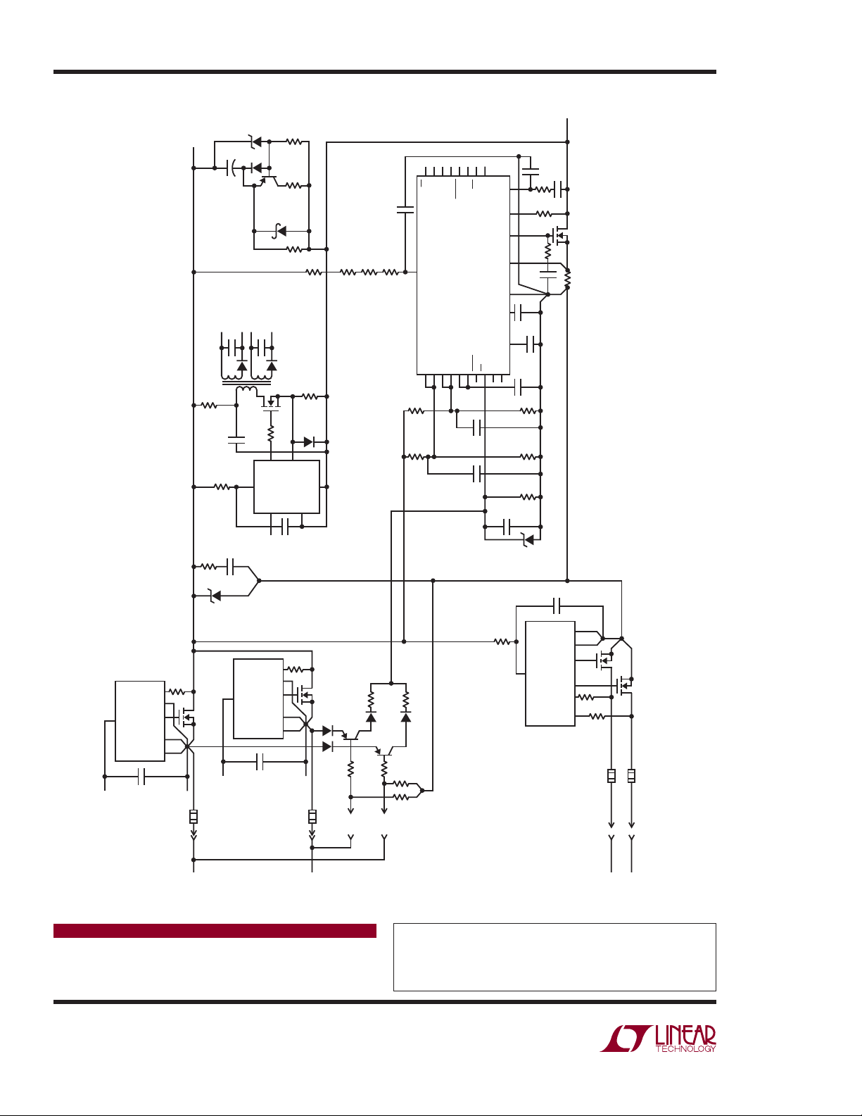
Figure 1 shows a complete circuit designed to handle up
to the maximum available power. The LTC4261’s accurate current limit is set to provide at least 5.5A under all
conditions, a comfortable margin for 200W, yet trips off
just under 7A to pr eserve fuse integrity in the presence
of nuisance overloads. At insertion the LTC4261 allows
contact bounce to settle, then soft starts the load using
a ramped current. Inrush current is increased gradually
to a few hundred milliamperes and held there until the
MOSFET is fully on.
Current is monitored by the SENSE pin and an 8mΩ shunt
resistor. Direct measurement of t he curren t is possible via
2
C port, with 10-bit resolution and 8A full scale.
the I
Cutting Diode Dissipation
ATCA’s redundant –48V power feeds are combined
on-card with ORing diodes. At 5A current consumption
even Schottky rectifi ers present a serious problem in
terms of both voltage drop and power dissipation: a
conducting pair drop more than 1V and dissipate 6W.
Following the diode manufacturer’s recommendations,
8 square inches of board area are needed to satisfy the
heat sinking requirements.
Diode dissipation, voltage loss and board area is reduced
in Figure 1 by using MOSFETs as active rectifi ers with
the LTC4354 diode OR driver. Total dissipation is cut to
less than 1W for two conducting “diodes” at maximum
load.
Zero Volt Transient
The so-called Zero Volt Transient requirement is a legacy
of earlier tele com equipment standards st ipulating uninterrupted system operation during the course of a 5ms input
voltage dropout. An energy of 1J is needed to sustain a
200W load during this interval.
The accepted method of energy storage to satisfy the 1J
requirement is a bulk reser voir capacitor which is charge d
through resistor s. This technique dictates the us e of bulky
high voltage stor age capacitors, such as 100V (or rare 80V )
rated unit s which can handle the ma ximum input voltage of
75V. Since the zero volt transient test commences at 44V,
nothing is gained by storing a higher voltage. Compact
50V capacitors are used instead, by limiting the charging
voltage with a simple zener-transistor circuit.
The ATCA connector pin confi guration presents a special
design challenge. Here extraction is inferred from the difference between each ENABLE and its associated VRTN,
thereby ignoring input dropouts. A PNP transistor pulls
up on EN in the event of an ENABLE disconnect, shutting
down the LTC4261 and permitting safe extraction with
no connector damage. During a zero volt transient, no
signal reaches the EN pin; power fl ows uninterrupted to
the load when the input voltage recovers.
, LT, LTC and LTM are registered trademarks of Linear Technology Corporation.
Hot Swap is a trademark of Linear Technology Corporation.
All other trademarks are the property of their respective owners.
09/06/397
–48VRTN(OUT)
PULSE
–
•••
P0926
100Ω
100nF
1mF
+
DB
V
100V
50V
1μF
D
×4
+
DB
V
BZT52C47
D
–
DA
V
1μF
D
ZVN3320F
FMMT591
+
DA
V
100Ω
8.2k
2.4k
×7
PDS5100H
10k
33Ω
D
1.1k
1.1k
1.1k
1.1k
–48VOUT
DN397 F01
33nF
10nF
330nF
2.49k
10.2k
47nF
10Ω
100V
1k
1M
IRF1310NS
8mΩ
C Current and Voltage Monitor
2
PG
SCL
1μF
IN
V
UVH
UVL
137k 107k
SDAI
SDAO
ADIN2OVON
PGI
PGIO
ALERT
LTC4261CGN
CC
FLTINENADR1
INTV
100nF
ADIN
RAMP
SENSE
EE
V
TMR GATE DRAIN
SS
ADR0
330nF
100nF
CC
V
/RUN NGATE
TH
I
NC
DADB
GA
LTC4354CS8
SS
V
SS
V
1μF
SENSE
LTC3803ES6
1μF
2k
FB
V
–
V
10A
LONG
DB
GND
FDS3672
DD
FMMT5401
100k
SHORT
100k
D
FMMT5401
100k
SHORT
D
100k
10k
100nF
100k
HZS5C1
CC
V
1μF
SS
V
SS
V
GB
GA
LTC4354CS8
DBDA
D: 1N4148WS
2k
2k
7A
MEDIUM LONG
FDS3672
FDS3672
Figure 1. AdvancedTCA Hot Swap Controller with I
7A
MEDIUM SHORT
100nF
1M1M
22k
22nF
100V
91Ω
SMBT70A
2k
DADB
GA
CC
V
LTC4354CS8
SS
V
SS
V
+
1μF
DA
V
–
DA
V
10A
LONG
FDS3672
CC
V
+
DB
V
VRTN_A
Data Sheet Download
www.linear.com
Linear Technology Corporation
1630 McCarthy Blvd., Milpitas, CA 95035-7417
(408) 432-1900
●
FAX: (408) 434-0507 ● www.linear.com
ENABLE_B
VRTN_B
ENABLE_A
–48V_A
–48V_B
For applications help,
call (408) 432-1900, Ext. 2452
dn3mlf LT/TP 0906 305K • PRINTED IN THE USA
© LINEAR TECHNOLOGY CORPORATION 2006
 Loading...